

Philips ISP1107W, ISP1107DH, ISP1107, ISP1106W, ISP1105 Datasheet
...
ISP1105/1106/1107
Advanced Universal Serial Bus transceivers
Rev. 06 — 30 November 2001 Product data
1. General description
The ISP1105/1106/1107 range of Universal Serial Bus (USB) transceivers are fully
compliant with the
portable electronics devices such as mobile phones, digital still cameras, Personal
Digital Assistants (PDA) and Information Appliances (IA).
They allow USB Application Specific ICs (ASICs) and Programmable Logic Devices
(PLDs) with power supply voltages from 1.65 V to 3.6 V to interface with the physical
layer of the Universal Serial Bus. They have an integrated 5 V to 3.3 V voltage
regulator for direct powering via the USB supply V
The ISP1105/1106/1107 range can be used as a USB device transceiver or a USB
host transceiver. They can transmit and receive serial data at both full-speed
(12 Mbit/s) and low-speed (1.5 Mbit/s) data rates.
ISP1105 allows single/differential input modes selectable by a MODE input and it is
available in HBCC16 package. ISP1106 allows only differential input mode and is
available in both TSSOP16 and HBCC16 packages. ISP1107 allows only
single-ended input mode and is available in both TSSOP16 and HBCC16 packages.
Universal Serial Bus Specification Rev. 1.1
.
BUS
. They are ideal for
2. Features
■ Complies with
■ Integrated bypassable 5 V to 3.3 V voltage regulator for powering via USB V
■ V
■ Used as a USB device transceiver or a USB host transceiver
■ Supports full-speed (12 Mbit/s) and low-speed (1.5 Mbit/s) serial data rates
■ Stable RCV output during SE0 condition
■ Two single-ended receivers with hysteresis
■ Low-power operation
■ Supports an I/O voltage range from 1.65 V to 3.6 V
■ 4 kV on-chip ESD protection
■ Full industrial operating temperature range −40 to +85 °C
■ Available in small TSSOP16 (except ISP1105) and HBCC16 packages.
disconnection indication through VP and VM
BUS
Universal Serial Bus Specification Rev. 1.1
BUS

Philips Semiconductors
3. Applications
■ Portable electronic devices, such as:
◆ Mobile phone
◆ Digital still camera
◆ Personal Digital Assistant (PDA)
◆ Information Appliance (IA).
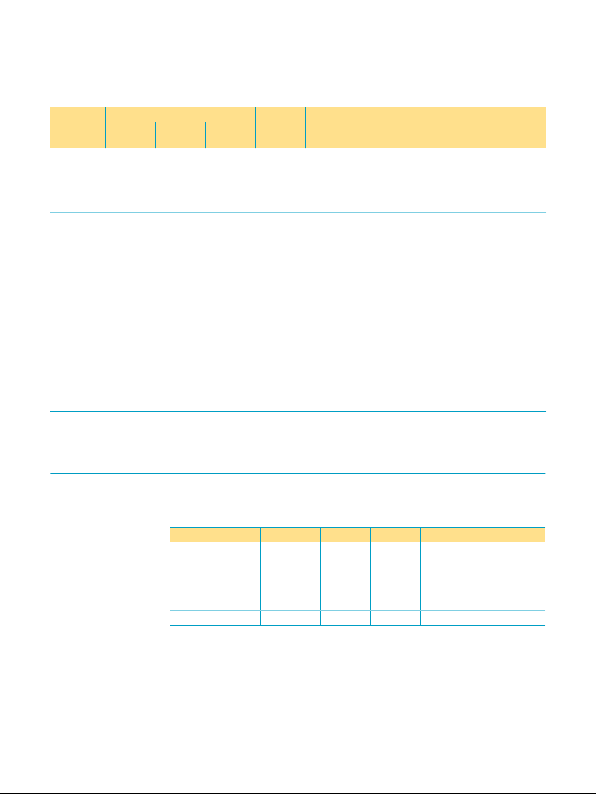
4. Ordering information
Table 1: Ordering information
Type number Package
Name Description Version
ISP1105W
ISP1106W
ISP1107W
ISP1106DH
ISP1107DH
[1]
HBCC16 plastic, heatsink bottom chip carrier; 16 terminals; body 3 × 3 × 0.65 mm SOT639-2
TSSOP16 plastic thin shrink small outline package; 16 leads; body width 4.4 mm SOT403-1
ISP1105/1106/1107
Advanced USB transceivers
[1] The ground terminal of ISP1105W is connected to the exposed diepad (heatsink).
4.1 Ordering options
Table 2: Selection guide
Product Package(s) Description
ISP1105 HBCC16 Supports both single-ended and differential input modes
ISP1106 TSSOP16 or HBCC16 Supports only the differential input mode
ISP1107 TSSOP16 or HBCC16 Supports only the single-ended input mode
[1] Refer to Table 5 and Table 6.
[2] Refer to Table 6.
[3] Refer to Table 5.
[2]
[3]
[1]
9397 750 08872
Product data Rev. 06 — 30 November 2001 2 of 24
© Koninklijke Philips Electronics N.V. 2001. All rights reserved.

Philips Semiconductors
5. Functional diagram
V
CC(I/O)
SOFTCON
SPEED
VMO/FSE0
VPO/VO
MODE
SUSPND
OE
RCV
VP
ISP1105/1106/1107
Advanced USB transceivers
3.3 V
VOLTAGE
REGULATOR
(3)
(3)
(4)
LEVEL
SHIFTER
ISP1105
ISP1106
ISP1107
V
V
V
pu(3.3)
D+
D−
CC(5.0)
reg(3.3)
33 Ω
33 Ω
(1)
(1)
(1%)
(1%)
1.5 kΩ
(2)
VM
MBL301
GND
(1) Use a 39 Ω resistor (1%) for a USB v2.0 compliant output impedance range.
(2) Connect to D− for low-speed operation.
(3) Pin function depends on device type see Section 7.2.
(4) Only for ISP1105.
Fig 1. Functional diagram (combined ISP1105, ISP1106 and ISP1107).
9397 750 08872
© Koninklijke Philips Electronics N.V. 2001. All rights reserved.
Product data Rev. 06 — 30 November 2001 3 of 24

Philips Semiconductors
6. Pinning information
6.1 Pinning
ISP1105/1106/1107
Advanced USB transceivers
SUSPND
VM
VP
RCV
OE
Bottom view
5
4
3
2
1
CC(I/O)
V
MODE
ISP1105W
GND
(exposed diepad)
141516
pu(3.3)
V
SOFTCON
SPEED
876
CC(5.0)
V
9
10
11
12
13
D−
D+
VPO/VO
VMO/FSE0
V
reg(3.3)
MBL303
SUSPND
VM
VP
RCV
OE
Bottom view
5
4
3
2
1
CC(I/O)
V
GND
ISP1106W
ISP1107W
pu(3.3)
V
SOFTCON
SPEED
876
*
141516
CC(5.0)
V
9
10
11
12
13
D−
D+
VPO/VO*
VMO/FSE0
V
reg(3.3)
MBL304
The asterisk (*) denotes that the signal names VO and
FSE0 apply to the ISP1107W.
Fig 2. Pinning diagram HBCC16 (ISP1105). Fig 3. Pinning diagram HBCC16 (ISP1106 and
ISP1107).
*
V
16
V
15
14
VMO/FSE0*
13
VPO/VO
12
D+
11
D−
10
SPEED
9
V
CC(5.0)
reg(3.3)
*
CC(I/O)
V
pu(3.3)
SOFTCON
OE
RCV
VP
VM
SUSPND
GND
1
2
3
4
ISP1106DH
ISP1107DH
5
6
7
8
MBL302
*
The asterisk (*) denotes that the signal names VO and FSE0 apply to the ISP1107DH.
Fig 4. Pinning diagram TSSOP16 (ISP1106 and ISP1107).
9397 750 08872
Product data Rev. 06 — 30 November 2001 4 of 24
© Koninklijke Philips Electronics N.V. 2001. All rights reserved.

Philips Semiconductors
ISP1105/1106/1107
Advanced USB transceivers
6.2 Pin description
Table 3: Pin description
CC(I/O)
[1]
Pin Type Description
ISP1105
HBCC16
ISP1106/7
HBCC16
ISP1106/7
TSSOP16
active LOW); enables the transceiver to transmit data on
the USB bus
); driven LOW when input SUSPND is HIGH; the
V
CC(I/O)
output state of RCV is preserved and stable during an SE0
condition
to V
); for external detection of single-ended zero
CC(I/O)
(SE0), error conditions, speed of connected device; driven
HIGH when no supply voltage is connected to V
V
reg(3.3)
to V
); for external detection of single-ended zero
CC(I/O)
(SE0), error conditions, speed of connected device; driven
HIGH when no supply voltage is connected to V
V
reg(3.3)
HIGH level enables low-power state while the USB bus is
inactive and drives output RCV to a LOW level
level enables the differential input mode (VPO, VMO)
whereas a LOW level enables a single-ended input mode
(VO, FSE0). see Table 5 and Table 6
[2]
6 8 - ground supply
779- supply voltage for digital I/O pins (1.65 to 3.6 V). When
V
is not connected, the (D+, D−) pins are in
CC(I/O)
three-state. This supply pin is totally independent of
V
CC(5.0)
and V
and must never exceed the V
reg(3.3)
voltage.
adjusts the slew rate of differential data outputs D+ and D−
according to the transmission speed:
LOW: low-speed (1.5 Mbit/s)
HIGH: full-speed (12 Mbit/s)
low-speed mode connect to pin V
full-speed mode connect to pin V
via a 1.5 kΩ resistor
pu(3.3)
via a 1.5 kΩ resistor
pu(3.3)
Schmitt trigger); see Table 5 and Table 6
Schmitt trigger); see Table 5 and Table 6
CC(I/O)
CC(I/O)
CC(I/O)
CC(5.0)
CC(5.0)
); a
); a HIGH
reg(3.3)
CC(I/O)
,
CC(I/O)
,
CC(I/O)
and
and
Symbol
OE113I input for output enable (CMOS level with respect to V
RCV224Odifferentialdatareceiveroutput(CMOSlevel with respect to
VP335Osingle-ended D+ receiver output (CMOS level with respect
VM446Osingle-ended D− receiver output (CMOS level with respect
SUSPND 557I suspend input (CMOS level with respect to V
MODE 6 I mode input (CMOS level with respect to V
GND V
SPEED 8 8 10 I speed selection input (CMOS levelwith respect to V
D− 9 9 11 AI/O negative USB data bus connection (analog, differential); for
D+ 10 10 12 AI/O positive USB data bus connection (analog, differential); for
VPO/VO 11 11 13 I driver data input (CMOS level with respect to V
VMO/FSE0 12 12 14 I driver data input (CMOS level with respect to V
,
);
9397 750 08872
Product data Rev. 06 — 30 November 2001 5 of 24
© Koninklijke Philips Electronics N.V. 2001. All rights reserved.
Philips Semiconductors
ISP1105/1106/1107
Advanced USB transceivers
Table 3: Pin description
Symbol
[1]
Pin Type Description
ISP1105
HBCC16
V
reg(3.3)
13 13 15 - Internalregulator option: regulated supply voltage output
…continued
ISP1106/7
HBCC16
ISP1106/7
TSSOP16
(3.0 to 3.6 V) during 5 V operation; a decoupling capacitor
of at least 0.1 µF is required
Regulator bypass option: used as a supply voltage input
for 3.3 V operation. (3.3 V ±10%)
V
CC(5.0)
14 14 16 - Internal regulator option: supply voltage input
(4.0 to 5.5 V); can be connected directly to USB supply
V
BUS
V
pu(3.3)
Regulator bypass option: connect to V
15 15 1 - pull-up supply voltage (3.3 V ±10%); connect an external
reg(3.3)
1.5 kΩ resistor on D+ (full-speed) or D− (low-speed); pin
function is controlled by input SOFTCON:
SOFTCON = LOW — V
floating (high impedance);
pu(3.3)
ensures zero pull-up current
SOFTCON = HIGH — V
to V
reg(3.3)
= 3.3 V;internally connected
pu(3.3)
SOFTCON 16 16 2 I software controlled USB connection input; a HIGH level
applies 3.3 V to pin V
, which is connected to an
pu(3.3)
external 1.5 kΩ pull-up resistor; this allows USB
connect/disconnect signalling to be controlled by software
[1] Symbol names with an overscore (e.g. NAME) indicate active LOW signals.
[2] Down bonded to the exposed diepad.
7. Functional description
7.1 Function selection
Table 4: Function table
SUSPND OE (D+, D−) RCV VP/VM Function
L L driving &
receiving
L H receiving
H L driving inactive
H H high-Z
[1] Signal levels on (D+, D−) are determined by other USB devices and external pull-up/down resistors.
[2] In ‘suspend’ mode (SUSPND = HIGH) the differential receiver is inactive and output RCV is always
LOW. Out-of-suspend (‘K’) signalling is detected via the single-ended receivers VP and VM.
[3] During suspend, the slew-rate control circuit of low-speed operation is disabled. The (D+, D−) lines
are still driven to their intended states, without slew-rate control. This is permitted because driving
during suspend is used to signal remote wake-up by driving a ‘K’ signal (one transition from idle to
‘K’ state) for a period of 1 to 15 ms.
[1]
[1]
inactive
active active normal driving
(differential receiver active)
active active receiving
[2]
active driving during ‘suspend’
(differential receiver inactive)
[2]
active low-power state
[3]
9397 750 08872
Product data Rev. 06 — 30 November 2001 6 of 24
© Koninklijke Philips Electronics N.V. 2001. All rights reserved.

Philips Semiconductors
7.2 Operating functions
Table 5: Driving function using single-ended input data interface (OE = L) [for
ISP1105/1106/1107
Advanced USB transceivers
ISP1107 and ISP1105 (MODE = L)]
FSE0 VO Data
L L differential logic 0
L H differential logic 1
H L SE0
H H SE0
Table 6: Driving function using differential input data interface (
and ISP1105 (MODE = H)]
VMO VPO Data
L L SE0
L H differential logic 1
H L differential logic 0
H H illegal state
Table 7: Receiving function (
(D+, D−) RCV VP
differential logic 0 L L H
differential logic 1 H H L
SE0 RCV*
[1] VP = VM = H indicates the sharing mode (V
[2] RCV* denotes the signal level on output RCV just before SE0 state occurs. This level is stable during
the SE0 period.
OE=H)
[2]
CC(5.0)/Vreg(3.3)
is disconnected).
OE = L) [for ISP1106
[1]
LL
7.3 Power supply configurations
The ISP1105/1106/1107 can be used with different power supply configurations,
which can be changed dynamically. An overview is given in Table 9.
VM
[1]
Normal mode — Both V
For 5 V operation, V
CC(5.0)
CC(I/O)
and V
CC(5.0)
or (V
CC(5.0)
and V
) are connected.
reg(3.3)
is connected to a 5 V source (4.0 to 5.5 V). The internal
voltage regulator then produces 3.3 V for the USB connections. For 3.3 V operation,
both V
CC(5.0)
and V
are connected to a 3.3 V source (3.0 to 3.6 V). V
reg(3.3)
CC(I/O)
is
independently connected to a voltage source (1.65 V to 3.6 V), depending on the
supply voltage of the external circuit.
Disable mode — V
is not connected, V
CC(I/O)
CC(5.0)
or (V
CC(5.0)
and V
reg(3.3)
) are
connected. In this mode, the internal circuits of the ISP1105/1106/1107 ensure that
the (D+, D−) pins are in three-state and the power consumption drops to the
low-power (suspended) state level. Some hysteresis is built into the detection of
V
Sharing mode — V
CC(I/O)
lost.
is connected, (V
CC(I/O)
CC(5.0)
and V
) are not connected. In
reg(3.3)
this mode, the (D+,D−) pins are made three-state and the ISP1105/1106/1107 allows
external signals of up to 3.6 V to share the (D+, D−) lines. The internal circuits of the
ISP1105/1106/1107 ensure that virtually no current (maximum 10 µA) is drawn via
the (D+, D−) lines. The power consumption through pin V
9397 750 08872
Product data Rev. 06 — 30 November 2001 7 of 24
© Koninklijke Philips Electronics N.V. 2001. All rights reserved.
CC(I/O)
drops to the

Philips Semiconductors
low-power (suspended) state level. Both the VP and VM pins are driven HIGH to
indicate this mode. Pin RCV is made LOW. Some hysteresis is built into the detection
of V
Table 8: Pin states in Disable or Sharing mode
Pins Disable mode state Sharing mode state
V
CC(5.0)/Vreg(3.3)
V
CC(I/O)
V
pu(3.3)
(D+, D−) high impedance high impedance
(VP, VM) invalid
RCV invalid
Inputs (VO/VPO, FSE0/VMO,
SPEED, MODE
SOFTCON)
[1] High impedance or driven LOW.
[2] ISP1105 only.
reg(3.3)
lost.
[2]
, SUSPND,OE,
ISP1105/1106/1107
Advanced USB transceivers
5 V input / 3.3 V output
3.3 V input / 3.3 V input
not present 1.65 V to 3.6 V input
high impedance (off) high impedance (off)
[1]
[1]
high impedance high impedance
not present
H
L
Table 9: Power supply configuration overview
V
CC(5.0)
V
reg(3.3)
or
V
CC(I/O)
Configuration Special characteristics
connected connected Normal mode connected not connected Disable mode (D+, D−) and V
pu(3.3)
impedance; VP, VM, RCV:
[1]
invalid
not connected connected Sharing mode (D+, D−) and V
pu(3.3)
impedance;
VP, VM driven HIGH;
RCV driven LOW
[1] High impedance or driven LOW.
7.4 Power supply input options
The ISP1105/1106/1107 range has two power supply input options:
Internal regulator — V
used to supply the internal circuitry with 3.3 V (nominal). The V
3.3 V output reference.
Regulator bypass — V
internal regulator is bypassed and the internal circuitry is supplied directly from the
V
power supply. The voltage range is 3.0 to 3.6 V to comply with the USB
reg(3.3)
specification.
is connected to 4.0 to 5.5 V. The internal regulator is
CC(5.0)
reg(3.3)
CC(5.0)
and V
are connected to the same supply. The
reg(3.3)
high
high
pin becomes a
The supply voltage range for each input option is specified in Table 10.
9397 750 08872
Product data Rev. 06 — 30 November 2001 8 of 24
© Koninklijke Philips Electronics N.V. 2001. All rights reserved.
 Loading...