

Page 1

查询ISP1104供应商
ISP1104
Advanced Universal Serial Bus transceiver
Rev. 02 — 14 October 2003 Product data
1. General description
2. Features
The ISP1104 Universal Serial Bus (USB) transceiver is compliant with the
Serial Bus Specification Rev. 2.0
full-speed (12 Mbit/s). It allows single and differential input modes selectable by a
MODE input.
It allows USB Application Specific Integrated Circuits (ASICs) and Programmable
Logic Devices (PLDs) with power supply voltages from 1.65 V to 3.6 V to interface
with the physical layer of the USB. It has an integrated 5 V-to-3.3 V voltage regulator
for direct powering via the USB supply line V
to detect the presence of the V
the D+ and D− pins can be shared with other serial protocols.
The ISP1104 is available in HBCC16 package.
The ISP1104 is ideal for use in portable electronic devices, such as mobile phones,
digital still cameras, personal digital assistants and information appliances.
■ Complies with
■ Supports full-speed (12 Mbit/s) serial data rate
■ Integrated 5 V-to-3.3 V voltage regulator for powering via USB line V
■ V
■ Used as USB device transceiver or USB transceiver
■ Stable RCV output during single-ended zero (SE0) condition
■ Two single-ended receivers with hysteresis
■ Low-power operation
■ Supports I/O voltage range from 1.65 V to 3.6 V
■ ±12 kV ESD protection at pins D+, D-, V
■ Full industrial operating temperature range from −40 °Cto+85 °C
■ Available in HBCC16 lead-free and halogen-free package.
voltage presence indication on pin VBUSDET
BUS
Universal Serial Bus Specification Rev. 2.0
. The ISP1104cantransmit and receive USB data at
. It has an integrated voltage detector
BUS
line voltage (V
BUS
CC(5.0)
). When V
CC(5.0)
and GND
BUS(VCC(5.0)
Universal
) is lost,
BUS
3. Applications
■ Portable electronic devices, such as:
◆ Mobile phone
◆ Digital Still Camera (DSC)
◆ Personal Digital Assistant (PDA)
◆ Information Appliance (IA).
Page 2
Philips Semiconductors
4. Ordering information
Table 1: Ordering information
Type
number
ISP1104W HBCC16 plastic thermal enhanced bottom chip carrier;
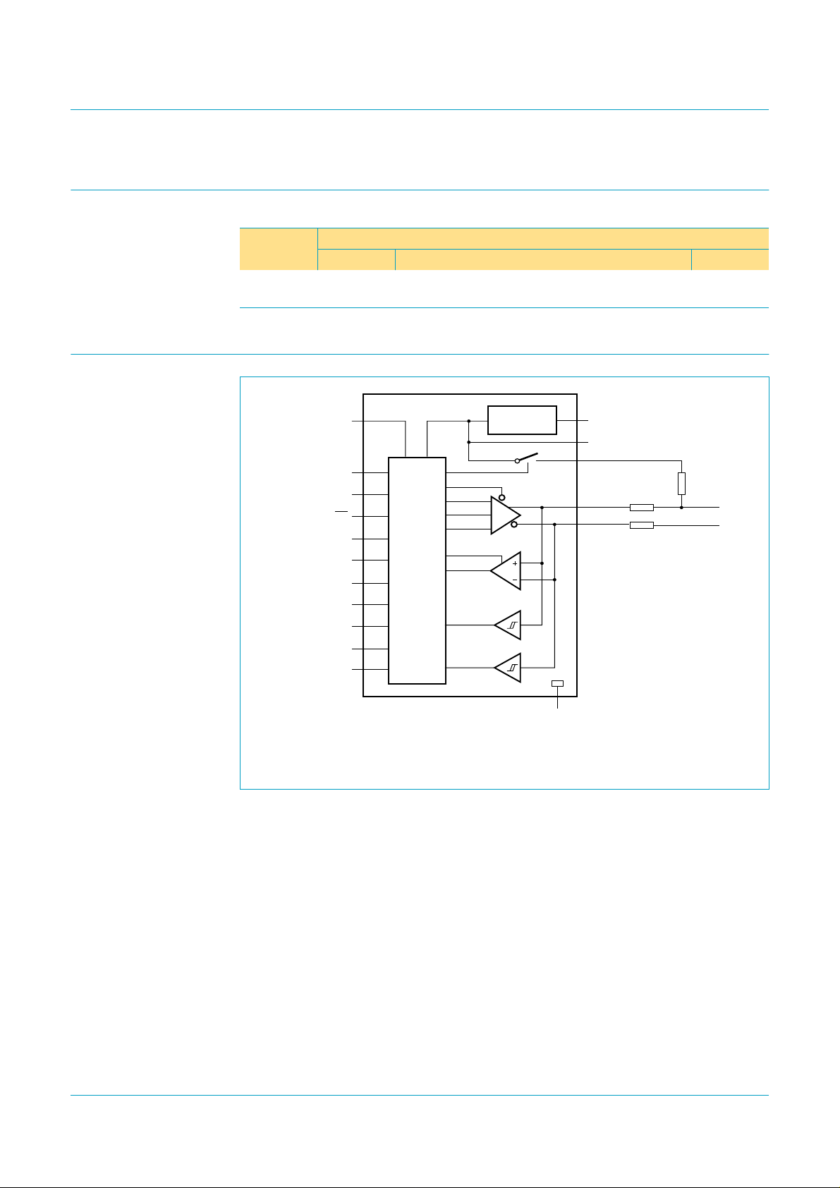
5. Block diagram
VMO/FSE0
ISP1104
Advanced USB transceiver
Package
Name Description Version
16 terminals; body 3 × 3 × 0.65 mm
3.3 V
V
CC(I/O)
VBUSDET
SOFTCON
OE
MODE
VPO/VO
SUSPND
RCV
VM
VP
(1)
(1)
LEVEL
SHIFTER
ISP1104
VOLTAGE
REGULATOR
V
V
V
pu(3.3)
D+
D−
CC(5.0)
reg(3.3)
33 Ω
33 Ω
(1%)
(1%)
SOT639-2
1.5 kΩ
GND
004aaa035
(1) Pin function depends on the device function, see Section 7.2.
Fig 1. Block diagram.
9397 750 11229
Product data Rev. 02 — 14 October 2003 2 of 19
© Koninklijke Philips Electronics N.V. 2003. All rights reserved.
Page 3
Philips Semiconductors
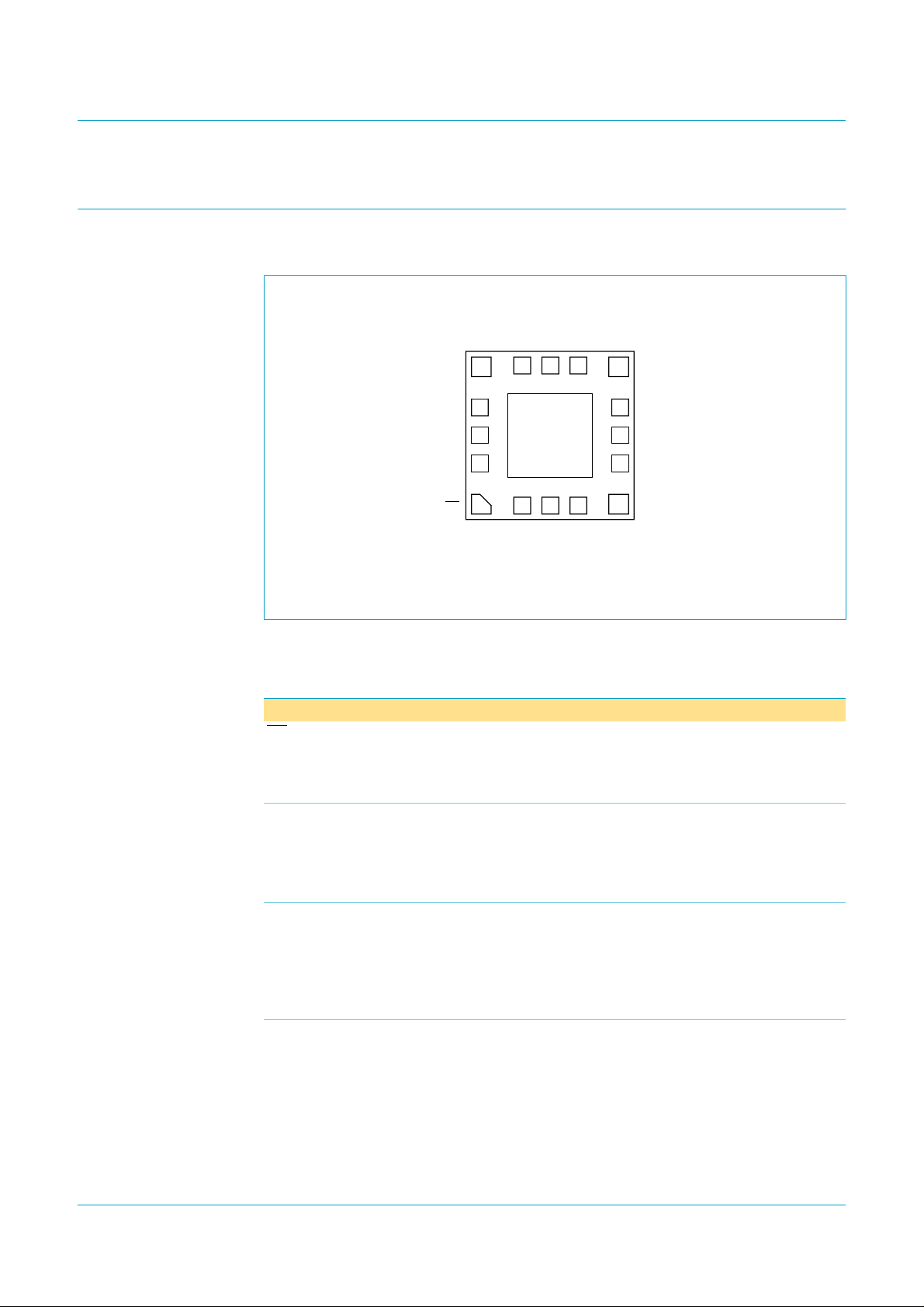
6. Pinning information
6.1 Pinning
SUSPND
ISP1104
Advanced USB transceiver
CC(I/O)
VBUSDET
V
MODE
5
876
D−
9
VM
VP
RCV
OE
Bottom view
4
3
2
1
ISP1104W
GND
(exposed diepad)
141516
pu(3.3)
V
SOFTCON
CC(5.0)
V
10
11
12
13
D+
VPO/VO
VMO/FSE0
V
reg(3.3)
004aaa036
Fig 2. Pin configuration HBCC16.
6.2 Pin description
Table 2: Pin description
Symbol
OE 1 I input for output enable (CMOS level with respect to
RCV 2 O differential data receiver output (CMOS level with respect
VP 3 O single-ended D+ receiver output (CMOS level with
VM 4 O single-ended D− receiver output (CMOS level with
[1]
Pin Type Description
, active LOW); enables the transceiver to transmit
V
CC(I/O)
data on the USB bus
input pad; push pull; CMOS
to V
); driven LOW when input SUSPND is HIGH;
CC(I/O)
the output state of RCV is preserved and stable during an
SE0 condition
output pad; push pull; 4 mA output drive; CMOS
respect to V
); for external detection of SE0, error
CC(I/O)
conditions and speed of connected device; driven HIGH
when no supply voltage is connected to V
V
reg(3.3)
output pad; push pull; 4 mA output drive; CMOS
respect to V
); for external detection of SE0, error
CC(I/O)
conditions and speed of connected device; driven HIGH
when no supply voltage is connected to V
V
reg(3.3)
output pad; push pull; 4 mA output drive; CMOS
CC(5.0)
CC(5.0)
and
and
9397 750 11229
Product data Rev. 02 — 14 October 2003 3 of 19
© Koninklijke Philips Electronics N.V. 2003. All rights reserved.
Page 4

Philips Semiconductors
ISP1104
Advanced USB transceiver
Table 2: Pin description
Symbol
[1]
Pin Type Description
SUSPND 5 I suspend input (CMOS level with respect to V
…continued
CC(I/O)
); a
HIGH level enables low-power state while the USB bus is
inactive and drives output RCV to a LOW level
input pad; push pull; CMOS
MODE 6 I mode input (CMOS level with respect to V
CC(I/O)
); a HIGH
level enables the differential input mode (pins VPO and
VMO) whereas a LOW levelenables a single-ended input
mode (pins VO and FSE0); see Table 4 and Table 5
input pad; push pull; CMOS
V
CC(I/O)
7 - supply voltage for digital I/O pins (1.65 V to 3.6 V); when
V
is not connected, the pins D+ and D− are in
CC(I/O)
three-state; this supply pin is totally independent of
V
CC(5.0)
and V
and must never exceed the V
reg(3.3)
reg(3.3)
voltage
VBUSDET 8 O V
indicator output (CMOS level with respect to
BUS
V
CC(I/O)
when V
); when V
< 3.6 V, then VBUSDET = LOW
BUS
> 4.1 V, then VBUSDET = HIGH and
BUS
output pad; push pull; 4 mA output drive; CMOS
D− 9 AI/O negative USB data bus connection (analog, differential)
D+ 10 AI/O positive USB data bus connection (analog, differential);
connect a 1.5 kΩ resistor to pin V
VPO/VO 11 I driver data input (CMOS level with respect to V
pu(3.3)
CC(I/O)
Schmitt trigger); see Table 4 and Table 5
input pad; push pull; CMOS
VMO/FSE0 12 I driver data input (CMOS level with respect to V
CC(I/O)
Schmitt trigger); see Table 4 and Table 5
input pad; push pull; CMOS
V
reg(3.3)
13 - regulated supply voltage output (3.0 V to 3.6 V); a
decoupling capacitor of at least 0.1 µF is required
V
CC(5.0)
V
pu(3.3)
14 - supply voltage input (4.0 V to 5.5 V); can be connected
directly to the USB supply line V
BUS
15 - pull-up supply voltage(3.3 V ± 10 %);connectan external
1.5 kΩ resistor on pin D+ (full-speed); pin function is
controlled by input SOFTCON
,
,
SOFTCON = LOW — V
floating (high impedance);
pu(3.3)
ensures zero pull-up current
SOFTCON = HIGH — V
connected to V
reg(3.3)
= 3.3 V; internally
pu(3.3)
SOFTCON 16 I software controlled USB connection input; a HIGH level
applies 3.3 V to pin V
, which is connected to an
pu(3.3)
external 1.5 kΩ pull-up resistor; this allows USB connect
or disconnect signalling to be controlled by software
input pad; push pull; CMOS
GND exposed
die pad
[1] Symbol names with an overscore (for example, NAME) indicate active LOW signals.
9397 750 11229
Product data Rev. 02 — 14 October 2003 4 of 19
- ground supply; down bonded to the exposed die pad
(heatsink); to be connected to the PCB ground
© Koninklijke Philips Electronics N.V. 2003. All rights reserved.
Page 5

Philips Semiconductors
7. Functional description
7.1 Function selection
Table 3: Function table
SUSPND OE D+ and D− RCV VP/VM Function
L L driving/
L H receiving
H L driving inactive
H H high-Z
[1] Signal levels on pins D+ and D− are determined by other USB devices and external pull-up or
pull-down resistors.
[2] In the suspend mode (pin SUSPND = HIGH), the differential receiver is inactive and the output RCV is
always LOW. Out-of-suspend (K) signalling is detected via the single-ended receivers VP and VM.
7.2 Operating functions
receiving
[1]
Advanced USB transceiver
active active normal driving
(differential receiver active)
[1]
active active receiving
[2]
active driving during ‘suspend’
(differential receiver inactive)
inactive
[2]
active low-power state
ISP1104
Table 4: Driving function using single-ended input data interface (pin OE = L and
pin MODE = L)
FSE0 VO Data
L L differential logic 0
L H differential logic 1
H L SE0
H H SE0
Table 5: Driving function using differential input data interface (pin
OE = L and
pin MODE = H)
VMO VPO Data
L L SE0
L H differential logic 1
H L differential logic 0
H H illegal state
Table 6: Receiving function (pin
D+ and D− RCV VP
OE=H)
[1]
VM
[1]
differential logic 0 L L H
differential logic 1 H H L
SE0 RCV*
[2]
LL
[1] VP = VM = H indicates the sharing mode (V
[2] RCV* denotes the signal level on output RCV just before the SE0 state occurs. This level is stable
during the SE0 period.
9397 750 11229
Product data Rev. 02 — 14 October 2003 5 of 19
is disconnected).
CC(5.0)
© Koninklijke Philips Electronics N.V. 2003. All rights reserved.
Page 6

Philips Semiconductors
7.3 Power supply configurations
The ISP1104 can be used with different power supply configurations, which can be
changed dynamically. Table 8 provides an overview of power supply configurations.
ISP1104
Advanced USB transceiver
Normal mode — Both V
V
is connected to a 5 V source (4.0 V to 5.5 V). The internal voltage regulator
CC(5.0)
then produces 3.3 V for USB connections. V
CC(I/O)
and V
are connected. For 5 V operation,
CC(5.0)
is independently connected to a
CC(I/O)
voltage source (1.65 V to 3.6 V), depending on the supply voltage of the external
circuit.
Disable mode — V
is not connected and V
CC(I/O)
is connected. In this mode,
CC(5.0)
the internal circuits of the ISP1104 ensure that the D+ and D− pins are in three-state
and the power consumption drops to the low-power (suspended) state level. Some
hysteresis is built into the detection of V
Sharing mode — V
is connected and V
CC(I/O)
the USB mode and other modes when sharing the V
CC(I/O)
lost.
CC(5.0)
< 3.6 V to differentiate between
. In this mode, pins D+ and
BUS
D− are made three-state and the ISP1104 allows external signals of up to 3.6 V to
share the D+ and D− lines. The internal circuits of the ISP1104 ensure that virtually
no current (maximum 10 µA) is drawn via the D+ and D− lines. The power
consumption through pin V
CC(I/O)
and pin V
drops to the low-power (suspended)
CC(5.0)
state level. Pins VP and VM are drivenHIGH and pins VBUSDET and RCV are driven
LOW to indicate this mode. Some hysteresis is built into the detection of V
Table 7: Pin states in disable or sharing mode
Pin Disable mode Sharing mode
V
CC(5.0)
V
reg(3.3)
V
CC(I/O)
V
pu(3.3)
D+, D− high impedance high impedance
VP, VM invalid
RCV invalid
VBUSDET invalid
VPO/VO, VMO/FSE0, MODE,
SUSPND,
OE, SOFTCON
5 V input <3.6 V
3.3 V output pulled-down
not present 1.65 V to 3.6 V input
high impedance (off) high impedance (off)
[1]
[1]
[1]
H
L
L
high impedance high impedance
CC(5.0)
lost.
[1] High impedance or driven LOW.
Table 8: Power supply configuration overview
V
CC(5.0)
V
CC(I/O)
Configuration Special characteristics
connected connected normal mode connected not connected disable mode D+, D− and V
VP, VM, RCV: invalid
not connected
or <3.6 V
connected sharing mode D+, D− and V
VP, VM driven HIGH; RCV driven
LOW; VBUSDET driven LOW; V
high impedance;
pu(3.3)
[1][2]
high impedance;
pu(3.3)
reg(3.3)
pulled-down
[1] High impedance or driven LOW.
[2] V
9397 750 11229
Product data Rev. 02 — 14 October 2003 6 of 19
may not be operational.
reg(3.3)
© Koninklijke Philips Electronics N.V. 2003. All rights reserved.
Page 7

Philips Semiconductors
8. Electrostatic discharge (ESD)
8.1 ESD protection
ISP1104
Advanced USB transceiver
The pins that are connected to the USB connector (D+, D−,V
and GND) have a
CC(5.0)
minimum of ±12 kV ESD protection. The ±12 kV measurement is limited by the test
equipment. Capacitors of 4.7 µF connected from V
reg(3.3)
to GND and V
CC(5.0)
to GND
are required to achieve this ±12 kV ESD protection (see Figure 3).
The ISP1104 can withstand ±12 kV using the Human Body Model and ±5 kV using
the Contact Discharge Method as specified in
R
C
1 MΩ
charge current
limit resistor
HIGH VOLTAGE
DC SOURCE
C
S
100 pF
Fig 3. Human Body ESD test model.
discharge
resistance
storage
capacitor
R
D
1500 Ω
IEC 61000-4-2
A
B
.
4.7 µF
DEVICE UNDER
TEST
V
CC(5.0)
V
reg(3.3)
4.7 µF
GND
004aaa145
8.2 ESD test conditions
A detailed report on test set-up and results is available on request.
9397 750 11229
Product data Rev. 02 — 14 October 2003 7 of 19
© Koninklijke Philips Electronics N.V. 2003. All rights reserved.
Page 8

Philips Semiconductors
ISP1104
Advanced USB transceiver
9. Limiting values
Table 9: Absolute maximum ratings
In accordance with the Absolute Maximum Rating System (IEC 60134).
Symbol Parameter Conditions Min Max Unit
V
CC(5.0)
V
CC(I/O)
V
I
I
lu
V
esd
T
stg
supply voltage −0.5 +6.0 V
I/O supply voltage −0.5 +4.6 V
DC input voltage −0.5 V
CC(I/O)
+ 0.5 V
latch-up current VI=−1.8 V to +5.4 V - 100 mA
electrostatic discharge voltage onpins D+,D−,V
CC(5.0)
[1][2]
−12000 +12000 V
and GND; ILI<1µA
on other pins; I
<1µA −2000 +2000 V
LI
storage temperature −40 +125 °C
[1] Testing equipment limits measurement to only ±12 kV. Capacitors needed on V
[2] Equivalent to discharging a 100 pF capacitor via a 1.5 kΩ resistor (Human Body Model).
CC(5.0)
and V
(see Section 8).
reg(3.3)
10. Recommended operating conditions
Table 10: Recommended operating conditions
Symbol Parameter Conditions Min Typ Max Unit
V
CC(5.0)
V
CC(I/O)
V
I
V
I(AI/O)
T
amb
supply voltage 4.0 5.0 5.5 V
I/O supply voltage 1.65 - 3.6 V
input voltage 0 - V
CC(I/O)
V
input voltage on AI/O pins pins D+ and D− 0 - 3.6 V
ambient temperature −40 - +85 °C
11. Static characteristics
Table 11: Static characteristics: supply pins
V
Symbol Parameter Conditions Min Typ Max Unit
V
I
I
I
I
I
I
I
= 4.0 V to 5.5 V; V
CC(5.0)
reg(3.3)
CC
CC(I/O)
CC(idle)
CC(I/O)(static)
CC(susp)
CC-I/O(dis)
CC(I/O)(sharing)
= 1.65 V to 3.6 V; V
CC(I/O)
regulated supply voltage output internal regulator option;
operating supply current transmitting and receiving at
=0V; T
GND
≤ 300 µA
I
load
12 Mbit/s; C
=−40°Cto+85°C; unless otherwise specified.
amb
[1][2]
3.0 3.3 3.6 V
[3]
-48mA
= 50 pF on
L
pins D+ and D−
operating I/O supply current transmitting and receiving at
[3]
-12mA
12 Mbit/s
supply current during full-speed
idle and SE0
idle: VD+> 2.7 V, VD−< 0.3 V;
SE0: V
< 0.3 V, VD−< 0.3 V
D+
[4]
- - 500 µA
static I/O supply current idle, SE0 or suspend - - 20 µA
suspend supply current SUSPND = H
disable current from VCC to
V
CC(I/O)
sharing mode I/O supply current V
V
not connected
CC(I/O)
not connected - - 20 µA
CC(5.0)
[4]
- - 100 µA
[4]
- - 100 µA
9397 750 11229
Product data Rev. 02 — 14 October 2003 8 of 19
© Koninklijke Philips Electronics N.V. 2003. All rights reserved.
Page 9

Philips Semiconductors
ISP1104
Advanced USB transceiver
Table 11: Static characteristics: supply pins
V
= 4.0 V to 5.5 V; V
CC(5.0)
= 1.65 V to 3.6 V; V
CC(I/O)
…continued
=0V; T
GND
=−40°Cto+85°C; unless otherwise specified.
amb
Symbol Parameter Conditions Min Typ Max Unit
I
Dx(sharing)
V
CC(5.0)th
sharing mode load current on
pins D+ and D−
supply voltage detection
threshold
V
not connected;
CC(5.0)
SOFTCON = L; V
1.65 V ≤ V
CC(I/O)
= 3.6 V
Dx
≤ 3.6 V
supply lost - - 3.6 V
-- 10µA
supply present 4.1 - - V
V
CC(5.0)hys
supply voltage detection
V
CC(I/O)
= 1.8 V - 70 - mV
hysteresis
V
CC(I/O)th
I/O supply voltage detection
threshold
V
= 2.7 V to 3.6 V
reg(3.3)
supply lost - - 0.5 V
supply present 1.4 - - V
V
CC(I/O)hys
I/O supply voltage detection
V
reg(3.3)
= 3.3 V - 0.45 - V
hysteresis
[1] I
[2] The minimum voltage is 2.7 V in the suspend mode.
[3] Characterized only, not tested in production.
[4] Excluding any load current and V
includes the pull-up resistor current via pin V
load
or Vsw source current to the 1.5 kΩ and 15 kΩ pull-up and pull-down resistors (200 µA typ.).
pu(3.3)
pu(3.3)
.
Table 12: Static characteristics: digital pins
V
= 1.65 V to 3.6 V; V
CC(I/O)
GND
=0V; T
=−40°Cto+85°C; unless otherwise specified.
amb
Symbol Parameter Conditions Min Typ Max Unit
V
= 1.65 V to 3.6 V
CC(I/O)
Input levels
V
IL
V
IH
LOW-level input voltage - - 0.3V
HIGH-level input voltage 0.6V
CC(I/O)
-- V
CC(I/O)
V
Output levels
V
OL
V
OH
LOW-level output voltage IOL= 100 µA - - 0.15 V
= 2 mA - - 0.4 V
I
OL
HIGH-level output voltage IOH= 100 µAV
= 2 mA V
I
OH
− 0.15 - - V
CC(I/O)
− 0.4 - - V
CC(I/O)
Leakage current
I
LI
input leakage current
[1]
−1-+1 µA
Capacitance
C
IN
Example 1: V
input capacitance pin to GND - - 10 pF
= 1.8 V ± 0.15 V
CC(I/O)
Input levels
V
IL
V
IH
LOW-level input voltage - - 0.5 V
HIGH-level input voltage 1.2 - - V
Output levels
V
OL
LOW-level output voltage IOL= 100 µA - - 0.15 V
= 2 mA - - 0.4 V
I
OL
9397 750 11229
Product data Rev. 02 — 14 October 2003 9 of 19
© Koninklijke Philips Electronics N.V. 2003. All rights reserved.
Page 10

Philips Semiconductors
ISP1104
Advanced USB transceiver
Table 12: Static characteristics: digital pins
V
= 1.65 V to 3.6 V; V
CC(I/O)
GND
=0V; T
amb
…continued
=−40°Cto+85°C; unless otherwise specified.
Symbol Parameter Conditions Min Typ Max Unit
V
OH
Example 2: V
HIGH-level output voltage IOH= 100 µA 1.5 - - V
= 2 mA 1.25 - - V
I
OH
= 2.5 V ± 0.2 V
CC(I/O)
Input levels
V
IL
V
IH
LOW-level input voltage - - 0.7 V
HIGH-level input voltage 1.7 - - V
Output levels
V
OL
V
OH
Example 3: V
LOW-level output voltage IOL= 100 µA - - 0.15 V
= 2 mA - - 0.4 V
I
OL
HIGH-level output voltage IOH= 100 µA 2.15 - - V
= 2 mA 1.9 - - V
I
OH
= 3.3 V ± 0.3 V
CC(I/O)
Input levels
V
IL
V
IH
LOW-level input voltage - - 0.9 V
HIGH-level input voltage 2.15 - - V
Output levels
V
OL
V
OH
LOW-level output voltage IOL= 100 µA - - 0.15 V
= 2 mA - - 0.4 V
I
OL
HIGH-level output voltage IOH= 100 µA 2.85 - - V
= 2 mA 2.6 - - V
I
OH
[1] If V
CC(I/O)
≥ V
, then the leakage current will be higher than the specified value.
reg(3.3)
Table 13: Static characteristics: analog I/O pins D+ and D−
V
= 4.0 V to 5.5 V; V
CC(5.0)
GND
=0V; T
=−40°Cto+85°C; unless otherwise specified.
amb
Symbol Parameter Conditions Min Typ Max Unit
Input levels
Differential receiver
V
DI
V
CM
differential input sensitivity |V
differential common mode
− V
I(D+)
| 0.2 - - V
I(D−)
includes VDI range 0.8 - 2.5 V
voltage
Single-ended receiver
V
IL
V
IH
V
hys
LOW-level input voltage - - 0.8 V
HIGH-level input voltage 2.0 - - V
hysteresis voltage 0.4 - 0.7 V
Output levels
V
OL
V
OH
LOW-level output voltage RL= 1.5 kΩ to +3.6 V - - 0.3 V
HIGH-level output voltage RL=15kΩ to GND
[1]
2.8 - 3.6 V
Leakage current
I
LZ
OFF-state leakage current −1- +1 µA
9397 750 11229
Product data Rev. 02 — 14 October 2003 10 of 19
© Koninklijke Philips Electronics N.V. 2003. All rights reserved.
Page 11

Philips Semiconductors
ISP1104
Advanced USB transceiver
Table 13: Static characteristics: analog I/O pins D+ and D−
V
= 4.0 V to 5.5 V; V
CC(5.0)
GND
=0V; T
=−40°Cto+85°C; unless otherwise specified.
amb
…continued
Symbol Parameter Conditions Min Typ Max Unit
Capacitance
C
IN
transceiver capacitance pin to GND - - 20 pF
Resistance
Z
DRV
Z
INP
R
SW
driver output impedance steady-state drive
input impedance 10 - - MΩ
internal switch resistance at
pin V
pu(3.3)
[2]
34 39 44 Ω
--10Ω
Termination
V
TERM
[1] V
OH(min)=Vreg(3.3)
[2] Includes external resistors of 33 Ω±1 % on both pins D+ and D−.
[3] This voltage is available at pins V
[4] The minimum voltage is 2.7 V in the suspend mode.
termination voltage for
upstream port pull-up (R
− 0.2 V.
reg(3.3)
)
pu
and V
pu(3.3)
.
[3][4]
3.0 - 3.6 V
12. Dynamic characteristics
Table 14: Dynamic characteristics: analog I/O pins D+ and D−
V
specified.
Symbol Parameter Conditions Min Typ Max Unit
Driver characteristics
t
t
FRFM differential rise/fall time
V
Driver timing
t
t
t
t
= 4.0 V to 5.5 V; V
CC(5.0)
FR
FF
CRS
PLH(drv)
PHL(drv)
PHZ
PLZ
= 1.65 V to 3.6 V; V
CC(I/O)
GND
=0V; T
amb
rise time CL= 50 pF to 125 pF;
10%to90%of|V
OH
see Figure 4
fall time CL= 50 pF to 125 pF;
90%to10%of|V
OH
see Figure 4
excluding the first transition
matching (t
output signal crossover
voltage
driver propagation delay
FR/tFF
)
from idle state
excluding the first transition
from idle state; see Figure 5
LOW-to-HIGH; seeFigure 5 --18ns
(VPO/VO, VMO/FSE0 to
D+,D−)
driver propagation delay
HIGH-to-LOW; see Figure 5 --18ns
(VPO/VO, VMO/FSE0 to
D+,D−)
driver disable delay (OE to
HIGH-to-OFF; see Figure 6 --15ns
D+, D−)
driver disable delay
OE to D+, D−)
(
LOW-to-OFF; seeFigure 6 --15ns
=−40°Cto+85°C; see Figure 8; unless otherwise
4 - 20 ns
− VOL|;
4 - 20 ns
− VOL|;
90 - 111.1 %
[1]
1.3 - 2.0 V
9397 750 11229
Product data Rev. 02 — 14 October 2003 11 of 19
© Koninklijke Philips Electronics N.V. 2003. All rights reserved.
Page 12

Philips Semiconductors
ISP1104
Advanced USB transceiver
Table 14: Dynamic characteristics: analog I/O pins D+ and D−
V
= 4.0 V to 5.5 V; V
CC(5.0)
= 1.65 V to 3.6 V; V
CC(I/O)
GND
=0V; T
…continued
=−40°Cto+85°C; see Figure 8; unless otherwise
amb
specified.
Symbol Parameter Conditions Min Typ Max Unit
t
PZH
t
PZL
driver enable delay
OE to D+, D−)
(
driver enable delay
OE to D+,D−)
(
OFF-to-HIGH; see Figure 6 --15ns
OFF-to-LOW; see Figure 6 --15ns
Receiver timings
Differential receiver
t
PLH(rcv)
propagation delay
LOW-to-HIGH; seeFigure 7 --15ns
(D+,D− to RCV)
t
PHL(rcv)
propagation delay
HIGH-to-LOW; see Figure 7 --15ns
(D+,D− to RCV)
Single-ended receiver
t
PLH(se)
propagation delay
LOW-to-HIGH; seeFigure 7 --18ns
(D+,D− to VP, VM)
t
PHL(se)
propagation delay
HIGH-to-LOW; see Figure 7 --18ns
(D+,D− to VP, VM)
[1] Characterized only, not tested. Limits guaranteed by design.
1.65 V
logic input
tFR, t
V
OH
V
OL
LR
90 %
10 %
90 %
tFF, t
10 %
LF
MGS963
0 V
V
OH
V
OL
differential
data lines
0.9 V
t
PLH(drv)
V
CRS
0.9 V
t
PHL(drv)
V
CRS
MGS964
Fig 4. Rise and fall times. Fig 5. Timing of VPO/VO and VMO/FSE0 to D+ and D−.
1.65 V
logic input
V
V
0 V
OH
differential
data lines
OL
0.9 V
Fig 6. Timing of
0.9 V
t
t
V
PZH
PZL
CRS
t
PHZ
t
PLZ
V
−0.3 V
OH
V
+0.3 V
OL
MGS966
OE to D+ and D−. Fig 7. Timing of D+ and D− to RCV, VP and VM.
2.0 V
differential
data lines
0.8 V
V
OH
logic output
V
OL
V
CRS
t
PLH(rcv)
t
PLH(se)
0.9 V
V
CRS
t
PHL(rcv)
t
PHL(se)
0.9 V
MGS965
9397 750 11229
© Koninklijke Philips Electronics N.V. 2003. All rights reserved.
Product data Rev. 02 — 14 October 2003 12 of 19
Page 13

Philips Semiconductors
13. Test information
V
pu(3.3)
ISP1104
Advanced USB transceiver
D.U.T.
004aaa037
1.5 kΩ
D+/D−
33 Ω
test point
C
L
15 kΩ
Load capacitance CL= 50 pF (minimum or maximum timing).
Fig 8. Load on pins D+ and D−.
test point
V = 0 V for t
V=V
reg(3.3)
PZH
for t
and t
PZL
PHZ
and t
.
PLZ
D.U.T.
33 Ω
.
500 Ω
50 pF
V
MBL142
Fig 9. Load on pins D+ and D− for enable and disable times.
test point
D.U.T.
25 pF
MGS968
Fig 10. Load on pins VM, VP and RCV.
9397 750 11229
Product data Rev. 02 — 14 October 2003 13 of 19
© Koninklijke Philips Electronics N.V. 2003. All rights reserved.
Page 14

Philips Semiconductors
14. Package outline
ISP1104
Advanced USB transceiver
HBCC16: plastic thermal enhanced bottom chip carrier; 16 terminals; body 3 x 3 x 0.65 mm
terminal 1
index area
e
4
D
e
1
D
h
e
59
B
A
E
y
e
E
e
h
2
1
detail X
C
b
f
b
2
v
M
w
M
b
1
b
v
M
w
M
C
y
SOT639-2
ACCB
v
M
ACCB
w
M
3
v
M
ACCB
w
M
ACCB
1/2 e
4
113
1/2 e
DIMENSIONS (mm are the original dimensions)
A
max.
0.8
A
1bA2
0.10
0.05
0.7
0.6
UNIT
mm
OUTLINE
VERSION
SOT639-2 MO-217
b
1
0.33
0.33
0.27
0.27
IEC JEDEC JEITA
Fig 11. HBCC16 package outline.
16
3
e
3
0 2.5 5 mm
b
b
3
2
0.38
0.38
0.32
0.32
X
D
D
h
3.1
1.45
2.9
1.35
REFERENCES
3.1
2.9
scale
E
E
h
1.45
1.35
0.5
e
2.5
e
e
1
2
2.45
2.5
A
2
A
e
3
2.45
EUROPEAN
PROJECTION
A
1
we
v
f
4
0.23
0.08
0.17
yy
0.1 0.05 0.2
ISSUE DATE
01-11-13
03-03-12
1
9397 750 11229
© Koninklijke Philips Electronics N.V. 2003. All rights reserved.
Product data Rev. 02 — 14 October 2003 14 of 19
Page 15

Philips Semiconductors
15. Packaging
The ISP1104W (HBCC16 package) is delivered on a type A carrier tape, see
Figure 12. The tape dimensions are given in Table 15.
The reel diameter is 330 mm. The reel is made of polystyrene (PS) and is not
designed for use in a baking process.
The cumulative tolerance of 10 successive sprocket holes is ±0.02 mm. The camber
must not exceed 1 mm in 100 mm.
ISP1104
Advanced USB transceiver
Type A
4
Type B
4
P1
A0
direction of feed
A0
P1
direction of feed
K0
dth
W
B0
W
elongated
sprocket hole
B0
Fig 12. Carrier tape dimensions.
Table 15: Type A carrier tape dimensions for the ISP1104W
Dimension Value Unit
A0 3.3 mm
B0 3.3 mm
K0 1.1 mm
P1 8.0 mm
W 12.0 ± 0.3 mm
K0
MLC338
9397 750 11229
Product data Rev. 02 — 14 October 2003 15 of 19
© Koninklijke Philips Electronics N.V. 2003. All rights reserved.
Page 16

Philips Semiconductors
16. Additional soldering information
16.1 (H)BCC packages: footprint
The surface material of the terminals on the resin protrusion consists of a 4-layer
metal structure (Au, Pd, Ni and Pd). The Au + Pd layer (0.1 µm min.) ensures
solderability, the Ni layer (5 µm min.) prevents diffusion, and the Pd layer on top
(0.5 µm min.) ensures effective wire bonding.
Terminal PCB land Solder resist mask Stencil mask
Normal
b
1
b
1
0.05
ISP1104
Advanced USB transceiver
All dimensions in mm
0.05
Solder land
Solder resist
Corner
Cavity
b
b
2
b
2
E
h
D
h
b
b
2
b
2
E
h
D
h
0.05
0.05
0.05
0.05
0.05
0.1
(4×)
0.05
0.05
0.3 (8×)
Cavity: exposed die pad, either functioning as heatsink or as ground connection; only for HBCC packages.
Fig 13. (H)BCC footprint and solder resist mask dimensions.
16.2 (H)BCC packages: reflow soldering profile
The conditions for reflow soldering of (H)BCC packages are as follows:
For exact dimensions
see package outline
drawing (SOT639-2)
0.05
Stencil print thickness:
0.1 to 0.12 mm
Solder stencil
004aaa123
• Preheating time: minimum 90 s at T = 145 to 155 °C
• Soldering time: minimum 90 s (BCC) or minimum 100 s (HBCC) at T > 183 °C
• Peak temperature:
– Ambient temperature: T
amb(max)
– Device surface temperature: T
9397 750 11229
Product data Rev. 02 — 14 October 2003 16 of 19
= 260 °C
case(max)
= 255 °C.
© Koninklijke Philips Electronics N.V. 2003. All rights reserved.
Page 17

Philips Semiconductors
17. Revision history
Table 16: Revision history
Rev Date CPCN Description
02 20031014 - Product data (9397 750 11229)
Modifications:
• Changed USB 1.1 reference to USB 2.0; also added data transfer rates
• Section 2: updated
• Figure 1, Figure 8 and Figure 9: removed the figure note on 33 Ω
• Table 2: updated the description for pin 8; added pad details
• Section 7.3 sharing mode: updated the first sentence
• Table 8: updated
• Table 9: added a table note
• Table 11: changed I
• Table 13: removed Z
01 20020826 - Product data (9397 750 09784)
CC(dis)
DRV2
Advanced USB transceiver
to I
CC-I/O(dis)
, and also the relevant (old) table note 3.
; also, changed the description
ISP1104
9397 750 11229
Product data Rev. 02 — 14 October 2003 17 of 19
© Koninklijke Philips Electronics N.V. 2003. All rights reserved.
Page 18

Philips Semiconductors
18. Data sheet status
ISP1104
Advanced USB transceiver
Level Data sheet status
I Objective data Development This data sheet contains data from the objective specification for product development. Philips
II Preliminary data Qualification Thisdata sheet contains data from thepreliminary specification.Supplementary data willbe published
III Product data Production This data sheet contains data from the product specification. Philips Semiconductors reserves the
[1] Please consult the most recently issued data sheet before initiating or completing a design.
[2] The product status of the device(s) described in this data sheet may have changed since this data sheet was published. The latest information is available on the Internet at
URL http://www.semiconductors.philips.com.
[3] For data sheets describing multiple type numbers, the highest-level product status determines the data sheet status.
[1]
Product status
19. Definitions
Short-form specification — The data in a short-form specification is
extracted from a full data sheet with the same type number and title. For
detailed information see the relevant data sheet or data handbook.
Limiting values definition — Limiting values given are in accordance with
the Absolute Maximum Rating System (IEC 60134). Stress above one or
more of the limiting values may cause permanent damage to the device.
These are stress ratings only and operation of the device at these or at any
other conditions above those given in the Characteristics sections of the
specification is not implied. Exposure to limiting values for extended periods
may affect device reliability.
Application information — Applications that are described herein for any
of these products are for illustrative purposes only. Philips Semiconductors
make no representation or warranty that such applications will be suitable for
the specified use without further testing or modification.
[2][3]
Definition
Semiconductors reserves the right to change the specification in any manner without notice.
at a later date. PhilipsSemiconductors reserves the right to change thespecification without notice, in
order to improve the design and supply the best possible product.
right to make changes at any time in order to improvethe design, manufacturing and supply. Relevant
changes will be communicated via a Customer Product/Process Change Notification (CPCN).
20. Disclaimers
Life support — These products are not designed for use in life support
appliances, devices, or systems where malfunction of these products can
reasonably be expected to result in personal injury. Philips Semiconductors
customers using or selling these products for use in such applications do so
at their own risk and agree to fully indemnify Philips Semiconductors for any
damages resulting from such application.
Right to make changes — Philips Semiconductors reserves the right to
make changes in the products - including circuits, standard cells, and/or
software - described or contained herein in order to improve design and/or
performance. When the product is in full production (status ‘Production’),
relevant changes will be communicated via a Customer Product/Process
Change Notification (CPCN). Philips Semiconductors assumes no
responsibility or liability for the use of any of these products, conveys no
licence or title under any patent, copyright, or mask work right to these
products, andmakes no representationsor warranties thatthese products are
free from patent,copyright, or mask work right infringement,unless otherwise
specified.
Contact information
For additional information, please visit http://www.semiconductors.philips.com.
For sales office addresses, send e-mail to: sales.addresses@www.semiconductors.philips.com. Fax: +31 40 27 24825
9397 750 11229
Product data Rev. 02 — 14 October 2003 18 of 19
© Koninklijke Philips Electronics N.V. 2003. All rights reserved.
Page 19

Philips Semiconductors
Contents
1 General description. . . . . . . . . . . . . . . . . . . . . . 1
2 Features . . . . . . . . . . . . . . . . . . . . . . . . . . . . . . . 1
3 Applications. . . . . . . . . . . . . . . . . . . . . . . . . . . . 1
4 Ordering information. . . . . . . . . . . . . . . . . . . . . 2
5 Block diagram . . . . . . . . . . . . . . . . . . . . . . . . . . 2
6 Pinning information. . . . . . . . . . . . . . . . . . . . . . 3
6.1 Pinning . . . . . . . . . . . . . . . . . . . . . . . . . . . . . . . 3
6.2 Pin description . . . . . . . . . . . . . . . . . . . . . . . . . 3
7 Functional description . . . . . . . . . . . . . . . . . . . 5
7.1 Function selection. . . . . . . . . . . . . . . . . . . . . . . 5
7.2 Operating functions. . . . . . . . . . . . . . . . . . . . . . 5
7.3 Power supply configurations. . . . . . . . . . . . . . . 6
8 Electrostatic discharge (ESD). . . . . . . . . . . . . . 7
8.1 ESD protection . . . . . . . . . . . . . . . . . . . . . . . . . 7
8.2 ESD test conditions . . . . . . . . . . . . . . . . . . . . . 7
9 Limiting values. . . . . . . . . . . . . . . . . . . . . . . . . . 8
10 Recommended operating conditions. . . . . . . . 8
11 Static characteristics. . . . . . . . . . . . . . . . . . . . . 8
12 Dynamic characteristics . . . . . . . . . . . . . . . . . 11
13 Test information. . . . . . . . . . . . . . . . . . . . . . . . 13
14 Package outline . . . . . . . . . . . . . . . . . . . . . . . . 14
15 Packaging. . . . . . . . . . . . . . . . . . . . . . . . . . . . . 15
16 Soldering . . . . . . . . . . . . . . . . . . . . . . . . . . . . . 16
16.1 Introduction to soldering surface mount
packages . . . . . . . . . . . . . . . . . . . . . . . . . . . . 16
16.2 Reflow soldering . . . . . . . . . . . . . . . . . . . . . . . 16
16.3 Wave soldering. . . . . . . . . . . . . . . . . . . . . . . . 16
16.4 Manual soldering . . . . . . . . . . . . . . . . . . . . . . 17
16.5 Package related soldering information . . . . . . 17
17 Additional soldering information . . . . . . . . . . 19
17.1 (H)BCC packages: footprint . . . . . . . . . . . . . . 19
17.2 (H)BCC packages: reflow soldering profile. . . 19
18 Revision history. . . . . . . . . . . . . . . . . . . . . . . . 20
19 Data sheet status. . . . . . . . . . . . . . . . . . . . . . . 21
20 Definitions . . . . . . . . . . . . . . . . . . . . . . . . . . . . 21
21 Disclaimers. . . . . . . . . . . . . . . . . . . . . . . . . . . . 21
ISP1104
Advanced USB transceiver
© Koninklijke Philips Electronics N.V. 2003.
Printed in The Netherlands
All rights are reserved. Reproduction in whole or in part is prohibited without the prior
written consent of the copyright owner.
The information presented in this document does not form part of any quotation or
contract, is believed to be accurate and reliable and may be changed without notice. No
liability will be accepted by the publisher for any consequence of its use. Publication
thereof does not convey nor imply any license under patent- or other industrial or
intellectual property rights.
Date of release: 14 October 2003 Document order number: 9397 750 11229
 Loading...