

Philips irfp9140n DATASHEETS
PD - 9.1492A
PRELIMINARY
l Advanced Process Technology
l Dynamic dv/dt Rating
l 175°C Operating Temperature
l P-Channel
l Fast Switching
l Fully Avalanche Rated
Description
Fifth Generation HEXFETs from International Rectifier
utilize advanced processing techniques to achieve
extremely low on-resistance per silicon area. This
benefit, combined with the fast switching speed and
ruggedized device design that HEXFET Power
MOSFETs are well known for, provides the designer
with an extremely efficient and reliable device for use
in a wide variety of applications.
The TO-247 package is preferred for commercialindustrial applications where higher power levels
preclude the use of TO-220 devices. The TO-247 is
similar but superior to the earlier TO-218 package
because of its isolated mounting hole.
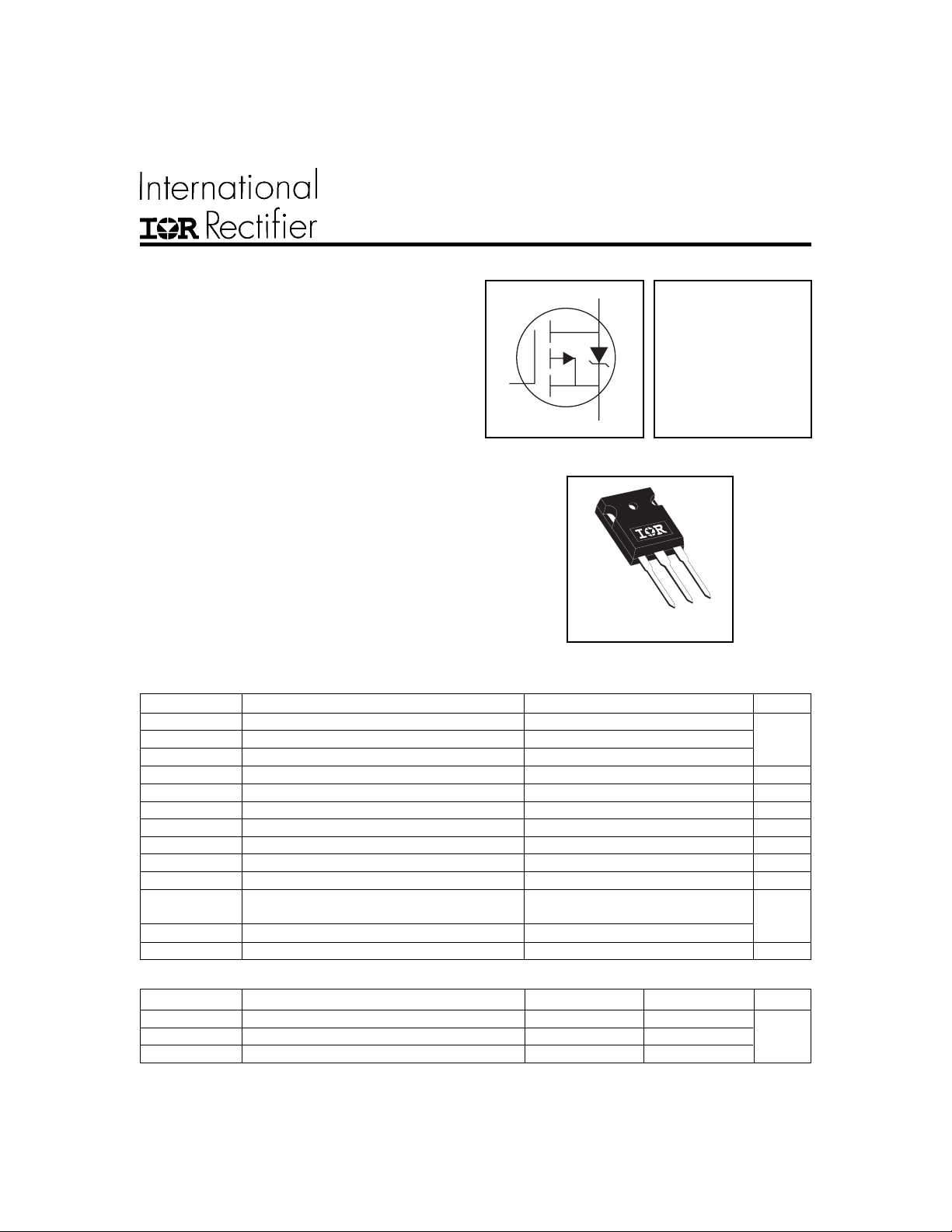
IRFP9140N
HEXFET® Power MOSFET
D
G
S
TO-247AC
V
R
DS(on)
DSS
= -100V
= 0.117Ω
ID = -23A
Absolute Maximum Ratings
Parameter Max. Units
ID @ TC = 25°C Continuous Drain Current, VGS @ -10V -23
ID @ TC = 100°C Continuous Drain Current, VGS @ -10V -16 A
I
DM
PD @TC = 25°C Power Dissipation 140 W
V
GS
E
AS
I
AR
E
AR
dv/dt Peak Diode Recovery dv/dt -5.0 V/ns
T
J
T
STG
Pulsed Drain Current -76
Linear Derating Factor 0.91 W/°C
Gate-to-Source Voltage ± 20 V
Single Pulse Avalanche Energy 430 mJ
Avalanche Current -11 A
Repetitive Avalanche Energy 14 mJ
Operating Junction and -55 to + 175
Storage Temperature Range
Soldering Temperature, for 10 seconds 300 (1.6mm from case )
Mounting torque, 6-32 or M3 screw 10 lbf•in (1.1N•m)
Thermal Resistance
Parameter Typ. Max. Units
R
θJC
R
θCS
R
θJA
Junction-to-Case ––– 1.1
Case-to-Sink, Flat, Greased Surface 0.24 ––– °C/W
Junction-to-Ambient ––– 40
°C
3/16/98
IRFP9140N
Electrical Characteristics @ TJ = 25°C (unless otherwise specified)
Parameter Min. Typ. Max. Units Conditions
V
(BR)DSS
∆V
(BR)DSS
R
DS(on)
V
GS(th)
g
fs
I
DSS
I
GSS
Q
g
Q
gs
Q
gd
t
d(on)
t
r
t
d(off)
t
f
L
D
L
S
C
iss
C
oss
C
rss
Drain-to-Source Breakdown Voltage -100 ––– ––– V VGS = 0V, ID = -250µA
/∆T
Breakdown Voltage Temp. Coefficient ––– -0.11 ––– V/°C Reference to 25°C, ID = -1mA
J
Static Drain-to-Source On-Resistance ––– ––– 0.117 Ω VGS = -10V, ID = -13A
Gate Threshold Voltage -2.0 ––– -4.0 V VDS = VGS, ID = -250µA
Forward Transconductance 5.3 ––– ––– S VDS = -50V, ID = 11A
Drain-to-Source Leakage Current
––– ––– -25
––– ––– -250 VDS = -80V, VGS = 0V, TJ = 150°C
Gate-to-Source Forward Leakage ––– ––– 100 VGS = 20V
Gate-to-Source Reverse Leakage ––– ––– -100
VDS = -100V, VGS = 0V
µA
nA
VGS = -20V
Total Gate Charge ––– ––– 97 ID = -11A
Gate-to-Source Charge ––– ––– 15 nC VDS = -80V
Gate-to-Drain ("Miller") Charge ––– ––– 51 VGS = -10V, See Fig. 6 and 13
Turn-On Delay Time ––– 15 ––– VDD = -50V
Rise Time ––– 67 ––– ID = -11A
Turn-Off Delay Time ––– 51 ––– RG = 5.1Ω
ns
Fall Time ––– 51 ––– RD = 4.2Ω, See Fig. 10
5.0
Internal Drain Inductance
Internal Source Inductance ––– –––
––– –––
13
Between lead,
6mm (0.25in.)
nH
from package
and center of die contact
Input Capacitance ––– 1300 ––– VGS = 0V
Output Capacitance ––– 400 ––– pF VDS = -25V
Reverse Transfer Capacitance ––– 240 ––– ƒ = 1.0MHz, See Fig. 5
D
G
S
Source-Drain Ratings and Characteristics
Parameter Min. Typ. Max. Units Conditions
I
S
I
SM
V
SD
t
rr
Q
rr
t
on
Notes:
Repetitive rating; pulse width limited by
max. junction temperature. ( See fig. 11 )
Starting T
RG = 25Ω, I
I
SD
TJ ≤ 175°C
Continuous Source Current MOSFET symbol
(Body Diode)
Pulsed Source Current integral reverse
(Body Diode)
––– –––
––– –––
Diode Forward Voltage ––– ––– -1.3 V TJ = 25°C, IS = -13A, VGS = 0V
Reverse Recovery Time ––– 150 220 ns TJ = 25°C, IF = -11A
Reverse RecoveryCharge ––– 830 1200 µC di/dt = -100A/µs
Forward Turn-On Time Intrinsic turn-on time is negligible (turn-on is dominated by LS+LD)
Pulse width ≤ 300µs; duty cycle ≤ 2%.
= 25°C, L = 7.1mH
J
= -11A. (See Figure 12)
AS
≤ -11A, di/dt ≤ -470A/µs, V
DD
≤ V
(BR)DSS
Uses IRF9540N data and test conditions
,
-23
-76
showing the
A
p-n junction diode.
D
G
S
IRFP9140N
A
A
A
)
A
100
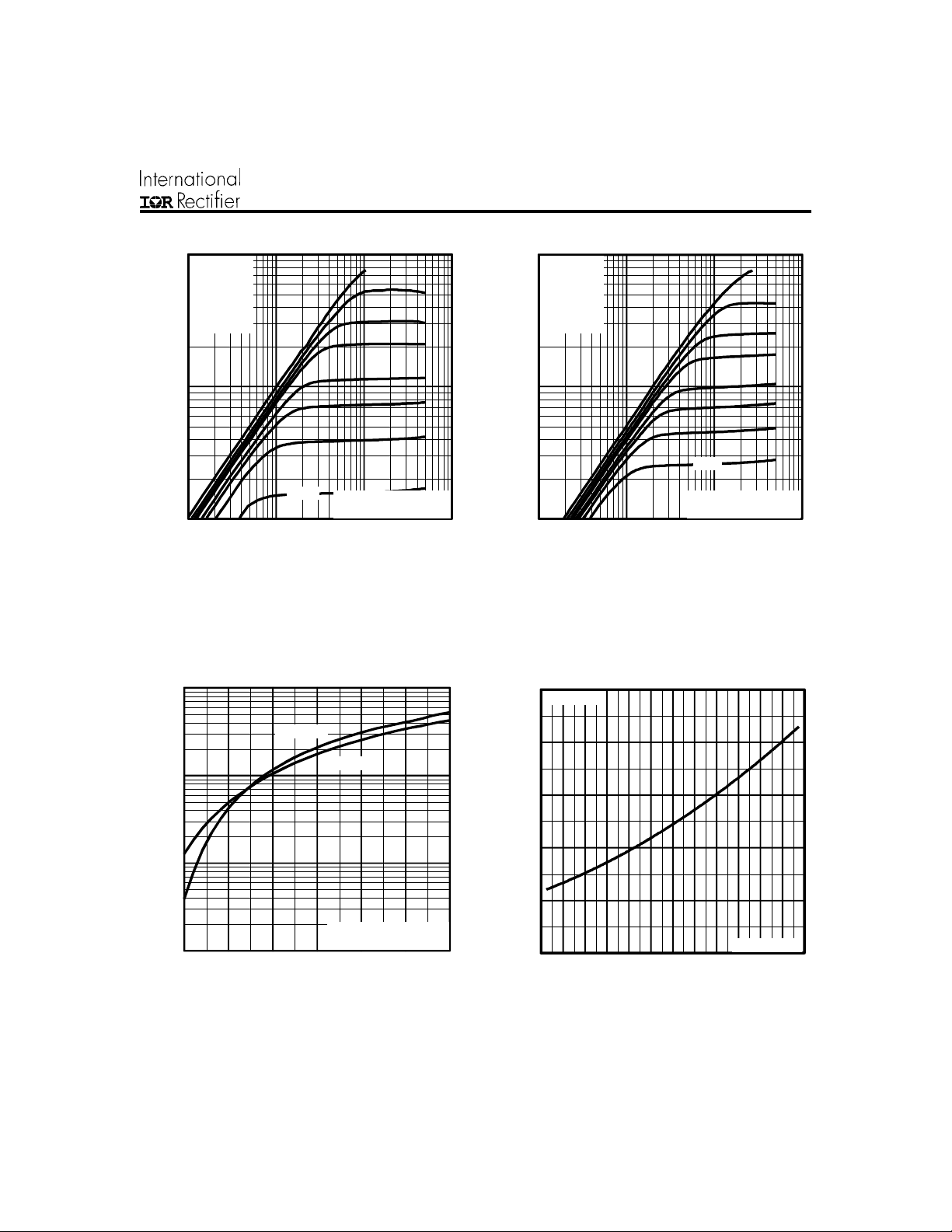
VGS
TOP - 15V
- 10V
- 8.0V
- 7.0V
- 6.0V
- 5.5V
- 5.0V
BOTTOM - 4.5V
10
D
-I , D ra in- to- S o ur ce Curre n t (A )
-4.5 V
1
0.1 1 10 100
-V , D ra in-to-Sourc e V o ltage (V)
DS
20µs PU LS E WIDTH
T = 25°C
c
Fig 1. Typical Output Characteristics
100
100
VGS
TOP - 15V
- 10V
- 8.0V
- 7.0V
- 6.0V
- 5.5V
- 5.0V
BOTTOM - 4.5V
10
D
-I , D ra in- to- S o ur ce C u rr en t (A )
-4.5 V
20µs PU LS E WIDTH
T = 175°C
1
0.1 1 10 1 00
-V , D ra in-to-S o u rce V o ltage (V )
DS
C
Fig 2. Typical Output Characteristics
2.5
I = -19A
D
T = 25°C
J
T = 175°C
10
1
D
-I , Dra in - to - S our c e Cur rent ( A )
0.1
45678910
-V , G a te - to -Source V o ltage (V
GS
J
V = -25V
DS
20µs PULSE W IDTH
2.0
1.5
1.0
(N o rmaliz e d)
0.5
DS(on)
R , D ra in -to -S o u rc e O n R e s is tan c e
0.0
-60 -40 -20 0 20 40 60 80 100 120 140 160 180
T , Junction Tem pe rature (°C)
J
Fig 3. Typical Transfer Characteristics Fig 4. Normalized On-Resistance
Vs. Temperature
V = -10 V
GS
 Loading...