

Philips IRFP460 Datasheet

Philips Semiconductors Product specification
PowerMOS transistors IRFP460
Avalanche energy rated
FEATURES SYMBOL QUICK REFERENCE DATA
• Repetitive Avalanche Rated
• Fast switching V
d
= 500 V
DSS
• Stable off-state characteristics
• High thermal cycling performance I
• Low thermal resistance
g
s
R
DS(ON)
= 20 A
D
≤ 0.27 Ω
GENERAL DESCRIPTION PINNING SOT429 (TO247)
N-channel, enhancement mode PIN DESCRIPTION
field-effect power transistor,
intendedforuse in off-line switched 1 gate
mode power supplies, T.V. and
computer monitor power supplies, 2 drain
d.c.tod.c.converters,motorcontrol
circuits and general purpose 3 source
switching applications.
The IRFP460 is supplied in the
tab drain
2
1
3
SOT429 (TO247) conventional
leaded package.
LIMITING VALUES
Limiting values in accordance with the Absolute Maximum System (IEC 134)
SYMBOL PARAMETER CONDITIONS MIN. MAX. UNIT
V
DSS
V
DGR
V
GS
I
D
I
DM
P
D
Tj, T
Drain-source voltage Tj = 25 ˚C to 150˚C - 500 V
Drain-gate voltage Tj = 25 ˚C to 150˚C; RGS = 20 kΩ - 500 V
Gate-source voltage - ± 30 V
Continuous drain current Tmb = 25 ˚C; VGS = 10 V - 20 A
Tmb = 100 ˚C; VGS = 10 V - 12.4 A
Pulsed drain current Tmb = 25 ˚C - 80 A
Total dissipation Tmb = 25 ˚C - 250 W
Operating junction and - 55 150 ˚C
stg
storage temperature range
AVALANCHE ENERGY LIMITING VALUES
Limiting values in accordance with the Absolute Maximum System (IEC 134)
SYMBOL PARAMETER CONDITIONS MIN. MAX. UNIT
E
AS
E
AR
IAS, I
1 pulse width and repetition rate limited by Tj max.
September 1999 1 Rev 1.000
Non-repetitive avalanche Unclamped inductive load, IAS = 20 A; - 1300 mJ
energy tp = 0.2 ms; Tj prior to avalanche = 25˚C;
VDD ≤ 50 V; RGS = 50 Ω; VGS = 10 V
Repetitive avalanche energy1IAR = 20 A; tp = 2.5 µs; Tj prior to - 32 mJ
avalanche = 25˚C; RGS = 50 Ω; VGS = 10 V
Repetitive and non-repetitive - 20 A
AR
avalanche current

Philips Semiconductors Product specification
PowerMOS transistors IRFP460
Avalanche energy rated
THERMAL RESISTANCES
SYMBOL PARAMETER CONDITIONS MIN. TYP. MAX. UNIT
R
th j-mb
R
th j-a
ELECTRICAL CHARACTERISTICS
Tj = 25 ˚C unless otherwise specified
SYMBOL PARAMETER CONDITIONS MIN. TYP. MAX. UNIT
V
(BR)DSS
∆V
(BR)DSS
∆T
j
R
DS(ON)
V
GS(TO)
g
fs
I
DSS
I
GSS
Q
g(tot)
Q
gs
Q
gd
t
d(on)
t
r
t
d(off)
t
f
L
d
L
d
L
s
C
iss
C
oss
C
rss
Thermal resistance junction - - 0.5 K/W
to mounting base
Thermal resistance junction SOT429 package, in free air - 45 - K/W
to ambient
Drain-source breakdown VGS = 0 V; ID = 0.25 mA 500 - - V
voltage
/ Drain-source breakdown VDS = VGS; ID = 0.25 mA - 0.1 - %/K
voltage temperature
coefficient
Drain-source on resistance VGS = 10 V; ID = 10 A - 0.2 0.27 Ω
Gate threshold voltage VDS = VGS; ID = 0.25 mA 2.0 3.0 4.0 V
Forward transconductance VDS = 30 V; ID = 10 A 13 18 - S
Drain-source leakage current VDS = 500 V; VGS = 0 V - 2 50 µA
VDS = 400 V; VGS = 0 V; Tj = 125 ˚C - 100 1000 µA
Gate-source leakage current VGS = ±30 V; VDS = 0 V - 10 200 nA
Total gate charge ID = 20 A; V
Gate-source charge - 12 18 nC
= 400 V; VGS = 10 V - 147 190 nC
DD
Gate-drain (Miller) charge - 78 100 nC
Turn-on delay time VDD = 250 V; RD = 12 Ω; - 23 - ns
Turn-on rise time RG = 3.9 Ω -72-ns
Turn-off delay time - 150 - ns
Turn-off fall time - 75 - ns
Internal drain inductance Measured from tab to centre of die - 3.5 - nH
Internal drain inductance Measured from drain lead to centre of die - 4.5 - nH
Internal source inductance Measured from source lead to source - 7.5 - nH
bond pad
Input capacitance VGS = 0 V; VDS = 25 V; f = 1 MHz - 3000 - pF
Output capacitance - 480 - pF
Feedback capacitance - 270 - pF
SOURCE-DRAIN DIODE RATINGS AND CHARACTERISTICS
Tj = 25 ˚C unless otherwise specified
SYMBOL PARAMETER CONDITIONS MIN. TYP. MAX. UNIT
I
S
I
SM
V
SD
t
rr
Q
rr
September 1999 2 Rev 1.000
Continuous source current Tmb = 25˚C - - 20 A
(body diode)
Pulsed source current (body Tmb = 25˚C - - 80 A
diode)
Diode forward voltage IS = 20 A; VGS = 0 V - - 1.5 V
Reverse recovery time IS = 20 A; VGS = 0 V; dI/dt = 100 A/µs - 900 - ns
Reverse recovery charge - 15 - µC
Philips Semiconductors Product specification
PowerMOS transistors IRFP460
Avalanche energy rated
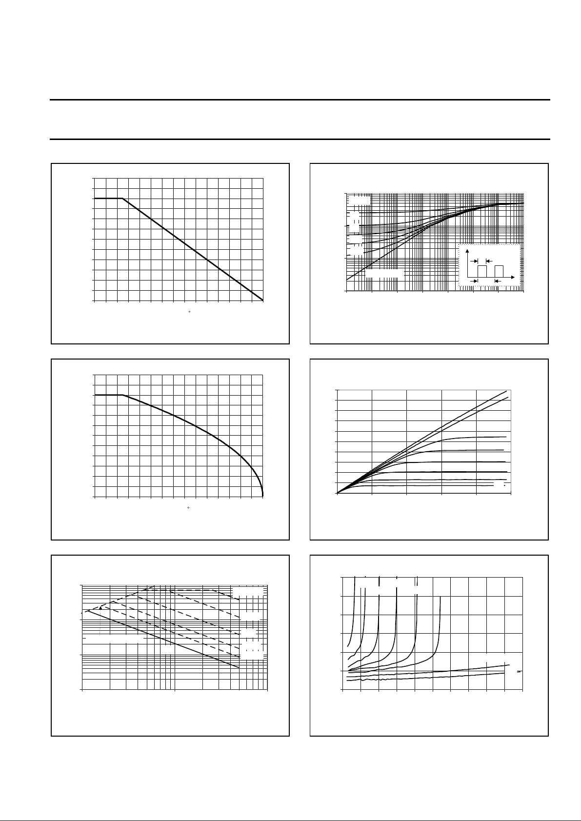
PD%
120
110
100
90
80
70
60
50
40
30
20
10
0
0 20 40 60 80 100 120 140
Normalised Power Derating
Tmb / C
Fig.1. Normalised power dissipation.
PD% = 100⋅PD/P
ID%
120
110
100
90
80
70
60
50
40
30
20
10
0
0 20 40 60 80 100 120 140
Tmb / C
= f(Tmb)
D 25 ˚C
Normalised Current Derating
Fig.2. Normalised continuous drain current.
ID% = 100⋅ID/I
= f(Tmb); conditions: VGS ≥ 10 V
D 25 ˚C
P
D
PHW20N50E
D = tp/T
tp
T
Zth j-mb (K/W)
1
D = 0.5
0.2
0.1
0.1
0.05
0.02
0.01
single pulse
0.001
1E-06 1E-05 1E-04 1E-03 1E-02 1E-01 1E+00 1E+01
Pulse width, tp (s)
Fig.4. Transient thermal impedance.
Z
= f(t); parameter D = tp/T
th j-mb
Drain Current, ID (A)
20
Tj = 25 C
18
16
14
12
10
8
6
4
2
0
012345
Drain-Source Voltage, VDS (V)
Fig.5. Typical output characteristics
ID = f(VDS); parameter V
PHW20N50E
VGS = 10 V
8 V
5 V
4.8 V
4.6 V
4.4 V
4.2 V
4 V
.
GS
Peak Pulsed Drain Current, IDM (A)
100
10
RDS(on) = VDS/ ID
1
0.1
10 100 1000
Drain-Source Voltage, VDS (V)
d.c.
PHW20N50E
tp = 10 us
100us
1 ms
10 ms
100 ms
Fig.3. Safe operating area. Tmb = 25 ˚C
ID & IDM = f(VDS); IDM single pulse; parameter t
Drain-Source On Resistance, RDS(on) (Ohms)
0.5
4V
4.2V
0.45
0.4
0.35
0.3
0.25
0.2
0 2 4 6 8 101214161820
4.6 V
4.4 V
4.8V
Drain Current, ID (A)
5V
Fig.6. Typical on-state resistance
R
p
= f(ID); parameter V
DS(ON)
PHW20N50E
Tj = 25 C
VGS = 6 V
10V
.
GS
September 1999 3 Rev 1.000
 Loading...