

Page 1
SERVICE MANUAL
BLU-RAY DISC HOME THEATER
HTS3106/F7 C
Page 2

IMPORTANT SAFETY NOTICE
Proper service and repair is important to the safe, reliable operation of all
P&F Equipment. The service procedures recommended by P&F and
described in this service manual are effective methods of performing
service operations. Some of these service special tools should be used
when and as recommended.
It is important to note that this service manual contains various CAUTIONS
and NOTICES which should be carefully read in order to minimize the risk
of personal injury to service personnel. The possibility exists that improper
service methods may damage the equipment. It also is important to
understand that these CAUTIONS and NOTICES ARE NOT EXHAUSTIVE.
P&F could not possibly know, evaluate and advice the service trade of all
conceivable ways in which service might be done or of the possible
hazardous consequences of each way. Consequently, P&F has not
undertaken any such broad evaluation. Accordingly, a servicer who uses a
service procedure or tool which is not recommended by P&F must first use
all precautions thoroughly so that neither his safety nor the safe operation
of the equipment will be jeopardized by the service method selected.
TABLE OF CONTENTS
Specifications . . . . . . . . . . . . . . . . . . . . . . . . . . . . . . . . . . . . . . . . . . . . . . . . . . . . . . . . . . . . . . . . . . . . . . . . . . 1-1-1
Laser Beam Safety Precautions . . . . . . . . . . . . . . . . . . . . . . . . . . . . . . . . . . . . . . . . . . . . . . . . . . . . . . . . . . . . 1-2-1
Important Safety Precautions . . . . . . . . . . . . . . . . . . . . . . . . . . . . . . . . . . . . . . . . . . . . . . . . . . . . . . . . . . . . . . 1-3-1
Standard Notes for Servicing . . . . . . . . . . . . . . . . . . . . . . . . . . . . . . . . . . . . . . . . . . . . . . . . . . . . . . . . . . . . . . 1-4-1
Cabinet Disassembly Instructions. . . . . . . . . . . . . . . . . . . . . . . . . . . . . . . . . . . . . . . . . . . . . . . . . . . . . . . . . . .1-5-1
How to Initialize the Blu-ray Disc Home Theater. . . . . . . . . . . . . . . . . . . . . . . . . . . . . . . . . . . . . . . . . . . . . . . .1-6-1
Firmware Renewal Mode . . . . . . . . . . . . . . . . . . . . . . . . . . . . . . . . . . . . . . . . . . . . . . . . . . . . . . . . . . . . . . . . . 1-7-1
Adjustment Instructions for BD Main CBA or BD Mechanism Assembly Replacement . . . . . . . . . . . . . . . . . . 1-8-1
Troubleshooting. . . . . . . . . . . . . . . . . . . . . . . . . . . . . . . . . . . . . . . . . . . . . . . . . . . . . . . . . . . . . . . . . . . . . . . . . 1-9-1
Error Message. . . . . . . . . . . . . . . . . . . . . . . . . . . . . . . . . . . . . . . . . . . . . . . . . . . . . . . . . . . . . . . . . . . . . . . . . 1-10-1
Block Diagram. . . . . . . . . . . . . . . . . . . . . . . . . . . . . . . . . . . . . . . . . . . . . . . . . . . . . . . . . . . . . . . . . . . . . . . . . 1-11-1
Schematic Diagrams and CBA . . . . . . . . . . . . . . . . . . . . . . . . . . . . . . . . . . . . . . . . . . . . . . . . . . . . . . . . . . . . 1-12-1
Waveforms . . . . . . . . . . . . . . . . . . . . . . . . . . . . . . . . . . . . . . . . . . . . . . . . . . . . . . . . . . . . . . . . . . . . . . . . . . .1-13-1
Wiring Diagram . . . . . . . . . . . . . . . . . . . . . . . . . . . . . . . . . . . . . . . . . . . . . . . . . . . . . . . . . . . . . . . . . . . . . . . . 1-14-1
Exploded Views. . . . . . . . . . . . . . . . . . . . . . . . . . . . . . . . . . . . . . . . . . . . . . . . . . . . . . . . . . . . . . . . . . . . . . . . 1-15-1
Mechanical Parts List . . . . . . . . . . . . . . . . . . . . . . . . . . . . . . . . . . . . . . . . . . . . . . . . . . . . . . . . . . . . . . . . . . .1-16-1
Electrical Parts List . . . . . . . . . . . . . . . . . . . . . . . . . . . . . . . . . . . . . . . . . . . . . . . . . . . . . . . . . . . . . . . . . . . . . 1-17-1
Manufactured under license from Dolby Laboratories.
Dolby and the double-D symbol are trademarks of Dolby Laboratories.
Page 3

SPECIFICATIONS
General
Signal system NTSC Color
Power requirements 120 V AC, 60 Hz
Power consumption 70 W (standby: 0.6 W)
Total output power (Amplifier) Home theater mode: 1000 W
Dimensions (width x height x depth) 17.2 x 2.4 x 11.7 inches (435 x 59 x 295.6 mm)
Weight Total weight: 24.03 lbs. (10.9 kg)
Operating temperature 41°F (5°C) to 104°F (40°C)
Operating humidity Less than 80 % (no condensation)
SD card slot
slot x 1
MP3 LINK jack
mini jack x 1 500 mVp-p (75:)
Analog audio output
(SPEAKERS (4:))
Front and rear speakers System: Full range satellite
Center speaker System: Full range satellite
Subwoofer Impedance: 4:
Video output
RCA jack x 1 1 Vp-p (75:)
Analog audio input (AUX)
RCA jacks(L / R) x 1 L/R: 2 Vrms (47k:)
Digital audio input (COAXIAL)
RCA jack x 1 500 mVp-p (75:)
HDMI output
HDMI jack x 1 Video: 480p, 720p, 1080i, 1080p, 1080p24/Audio
LAN terminal
Wireless LAN (Internal)
FTC* output power: 700 W
* (Main Ch @ 1 kHz within 10 % THD, Sub Ch 60 Hz within 2.5 % THD)
Main unit: 8.05 lbs. (3.65 kg)
Terminals
Impedance: 4:
Frequency response: 180 Hz ~ 20 kHz
Dimensions: 3.9 x 5.1 x 4.0 inches (100 x 130 x 100.5 mm)
Speaker cable length: front - 9.8 feet (3 m)
rear - 30 feet (9.15 m)
Weight: front - 1.19 lbs. (0.54 kg)
rear - 1.13 lbs. (0.51 kg)
Impedance: 4:
Frequency response: 180 Hz ~ 20 kHz
Dimensions: 3.9 x 5.1 x 4.0 inches (100 x 130 x 100.5 mm)
Speaker cable length: 9.8 feet (3 m)
Weight: 1.61 lbs. (0.73 kg)
Speaker drivers: 5.25 inches (130 mm) woofer
Frequency response: 60 Hz ~ 150 Hz
Dimensions: 6.1 x 11.8 x 7.8 inches (154 x 300.5 x 198 mm)
Speaker cable length: 14.1 feet (4.3 m)
Weight: 6.02 lbs. (2.73 kg)
10BASE-T / 100BASE-TX
IEEE 802.11 b/g/n
D Note
• The specifications and design of this product are subject to change without notice.
1-1-1 EDA02SP
Page 4
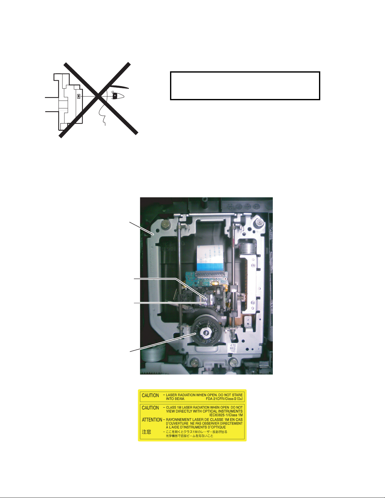
LASER BEAM SAFETY PRECAUTIONS
This BD player uses a pickup that emits a laser beam.
Do not look directly at the laser beam coming
from the pickup or allow it to strike against your
skin.
The laser beam is emitted from the location shown in the figure. When checking the laser diode, be sure to keep
your eyes at least 11.8 inches (30 cm) away from the pickup lens when the diode is turned on. Do not look directly
at the laser beam.
CAUTION: Use of controls and adjustments, or doing procedures other than those specified herein, may result in
hazardous radiation exposure.
Drive Mechanism Assembly
Laser Beam Radiation
Laser Pickup
Turntable
Location: Inside Top of BD mechanism.
1-2-1 HT3.5N_LBSP
Page 5

IMPORTANT SAFETY PRECAUTIONS
Product Safety Notice
Some electrical and mechanical parts have special
safety-related characteristics which are often not
evident from visual inspection, nor can the protection
they give necessarily be obtained by replacing them
with components rated for higher voltage, wattage,
etc. Parts that have special safety characteristics are
identified by a # on schematics and in parts lists. Use
of a substitute replacement that does not have the
same safety characteristics as the recommended
replacement part might create shock, fire, and/or other
hazards. The Product’s Safety is under review
continuously and new instructions are issued
whenever appropriate. Prior to shipment from the
factory, our products are carefully inspected to confirm
with the recognized product safety and electrical
codes of the countries in which they are to be sold.
However, in order to maintain such compliance, it is
equally important to implement the following
precautions when a set is being serviced.
Precautions during Servicing
A. Parts identified by the # symbol are critical for
safety. Replace only with part number specified.
B. In addition to safety, other parts and assemblies
are specified for conformance with regulations
applying to spurious radiation. These must also be
replaced only with specified replacements.
Examples: RF converters, RF cables, noise
blocking capacitors, and noise blocking filters, etc.
C. Use specified internal wiring. Note especially:
1) Wires covered with PVC tubing
2) Double insulated wires
3) High voltage leads
D. Use specified insulating materials for hazardous
live parts. Note especially:
1) Insulation tape
2) PVC tubing
3) Spacers
4) Insulators for transistors
E. When replacing AC primary side components
(transformers, power cord, etc.), wrap ends of
wires securely about the terminals before
soldering.
F. Observe that the wires do not contact heat
producing parts (heat sinks, oxide metal film
resistors, fusible resistors, etc.).
G. Check that replaced wires do not contact sharp
edges or pointed parts.
H. When a power cord has been replaced, check that
11~13 lb (5~6 kg) of force in any direction will not
loosen it.
I. Also check areas surrounding repaired locations.
J. Be careful that foreign objects (screws, solder
droplets, etc.) do not remain inside the set.
K. When connecting or disconnecting the internal
connectors, first, disconnect the AC plug from the
AC outlet.
L. When reassembling, be sure to use the original
screws or specified screws listed in the parts list.
M. This unit is classified as a CLASS 1 LASER
PRODUCT.
1-3-1 EDA02_ISP
Page 6
Safety Check after Servicing
Examine the area surrounding the repaired location for damage or deterioration. Observe that screws, parts, and
wires have been returned to their original positions. Afterwards, do the following tests and confirm the specified
values to verify compliance with safety standards.
1. Clearance Distance
When replacing primary circuit components, confirm
specified clearance distance (d) and (d’) between
soldered terminals, and between terminals and
surrounding metallic parts. (See Fig. 1)
Table 1: Ratings for selected area
Chassis or Secondary Conductor
Primary Circuit
AC Line Voltage Clearance Distance (d), (d’)
120 V
Note: This table is unofficial and for reference only. Be
sure to confirm the precise values.
≥ 3mm(d)
≥ 5.8mm(d’)
2. Leakage Current Test
Confirm the specified (or lower) leakage current
between B (earth ground, power cord plug prongs) and
externally exposed accessible parts (RF terminals,
antenna terminals, video and audio input and output
terminals, microphone jacks, earphone jacks, etc.) is
lower than or equal to the specified value in the table
below.
Measuring Method (Power ON):
Insert load Z between B (earth ground, power cord plug
prongs) and exposed accessible parts. Use an AC
voltmeter to measure across the terminals of load Z.
See Fig. 2 and the following table.
d' d
Exposed Accessible Part
Z
One side of
B
Power Cord Plug Prongs
Fig. 1
AC Voltmeter
(High Impedance)
Table 2: Leakage current ratings for selected areas
AC Line Voltage Load Z Leakage Current (i)
2kΩ RES.
Connected in
parallel
120 V
50kΩ RES.
Connected in
parallel
Note:This table is unofficial and for reference only. Be sure to confirm the precise values.
i≤0.7mA AC Peak
i≤2mA DC
i≤0.7mA AC Peak
i≤2mA DC
1-3-2 EDA02_ISP
One side of power cord plug
prongs (B) to:
RF or
Antenna terminals
A/V Input, Output
Fig. 2
Page 7
STANDARD NOTES FOR SERVICING
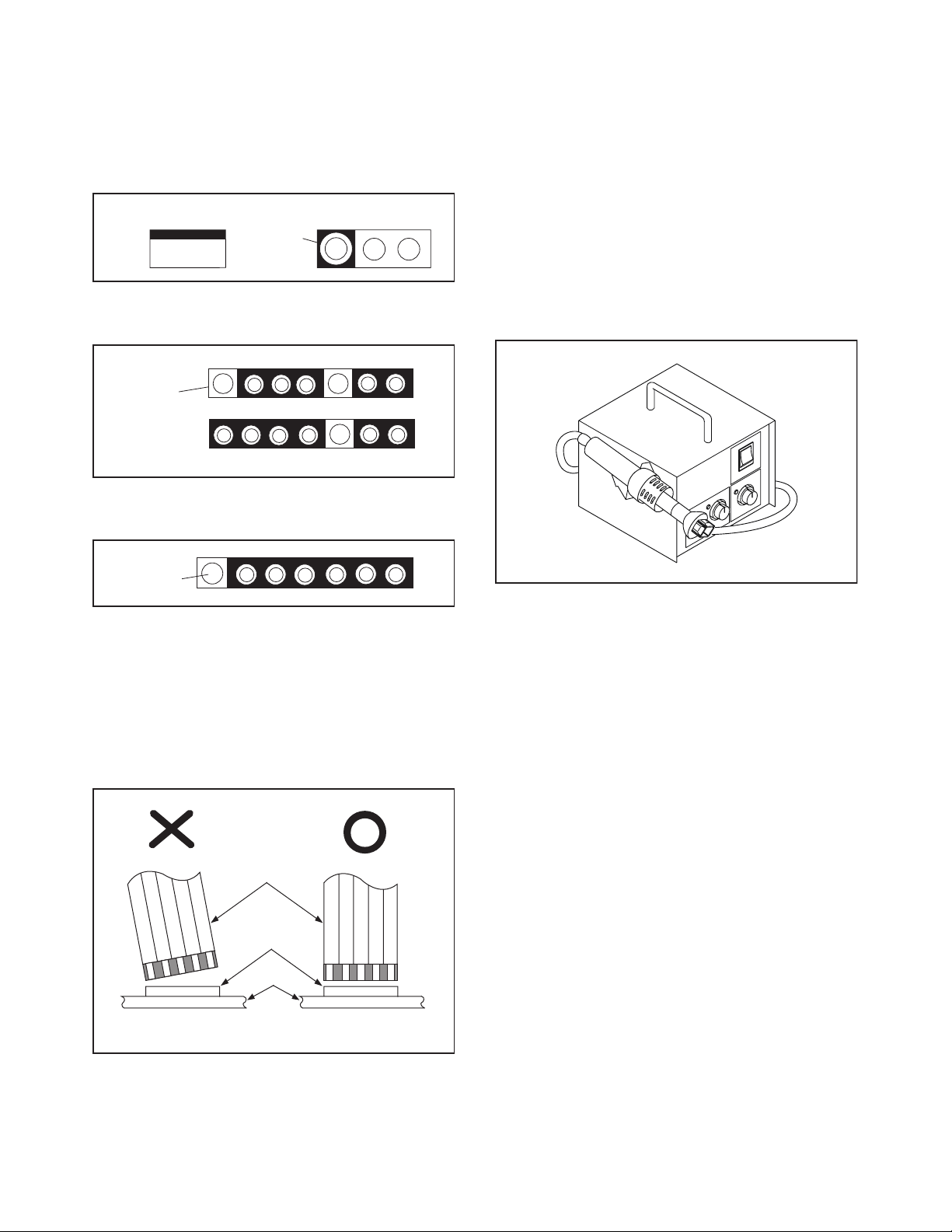
Circuit Board Indications
1. The output pin of the 3 pin Regulator ICs is
indicated as shown.
To p Vi ew
Out
2. For other ICs, pin 1 and every fifth pin are
indicated as shown.
Pin 1
3. The 1st pin of every male connector is indicated as
shown.
Pin 1
Input
In
Bottom View
5
10
Pb (Lead) Free Solder
When soldering, be sure to use the Pb free solder.
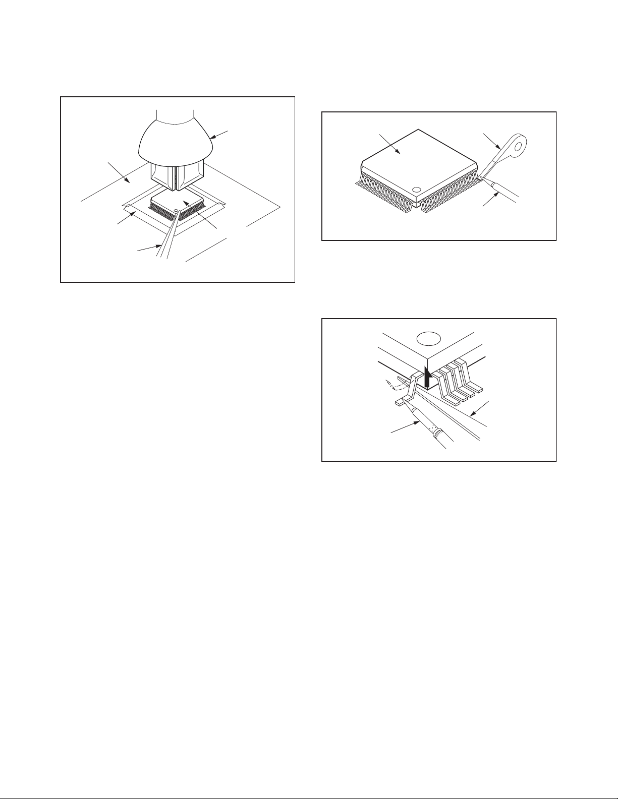
How to Remove / Install Flat Pack-IC
1. Removal
With Hot-Air Flat Pack-IC Desoldering Machine:
1. Prepare the hot-air flat pack-IC desoldering
machine, then apply hot air to the Flat Pack-IC
(about 5 to 6 seconds). (Fig. S-1-1)
Fig. S-1-1
Instructions for Connectors
1. When you connect or disconnect the FFC (Flexible
Foil Connector) cable, be sure to first disconnect
the AC cord.
2. FFC (Flexible Foil Connector) cable should be
inserted parallel into the connector, not at an
angle.
FFC Cable
Connector
CBA
* Be careful to avoid a short circuit.
2. Remove the flat pack-IC with tweezers while
applying the hot air.
3. Bottom of the flat pack-IC is fixed with glue to the
CBA; when removing entire flat pack-IC, first apply
soldering iron to center of the flat pack-IC and heat
up. Then remove (glue will be melted). (Fig. S-1-6)
4. Release the flat pack-IC from the CBA using
tweezers. (Fig. S-1-6)
CAUTION:
1. The Flat Pack-IC shape may differ by models. Use
an appropriate hot-air flat pack-IC desoldering
machine, whose shape matches that of the Flat
Pack-IC.
2. Do not supply hot air to the chip parts around the
flat pack-IC for over 6 seconds because damage
to the chip parts may occur. Put masking tape
around the flat pack-IC to protect other parts from
damage. (Fig. S-1-2)
1-4-1 BDN_SN
Page 8
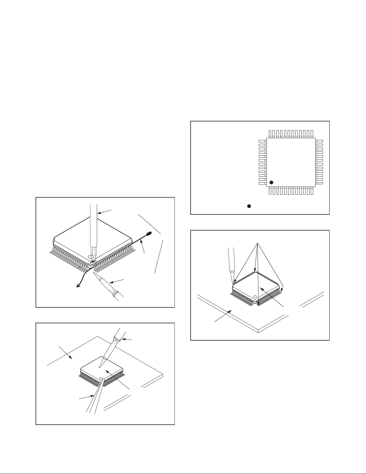
3. The flat pack-IC on the CBA is affixed with glue, so
be careful not to break or damage the foil of each
pin or the solder lands under the IC when
removing it.
With Soldering Iron:
1. Using desoldering braid, remove the solder from
all pins of the flat pack-IC. When you use solder
flux which is applied to all pins of the flat pack-IC,
you can remove it easily. (Fig. S-1-3)
CBA
Masking
Ta pe
Tweezers
Hot-air
Flat Pack-IC
Desoldering
Machine
Flat Pack-IC
Fig. S-1-2
Flat Pack-IC
Desoldering Braid
Soldering Iron
Fig. S-1-3
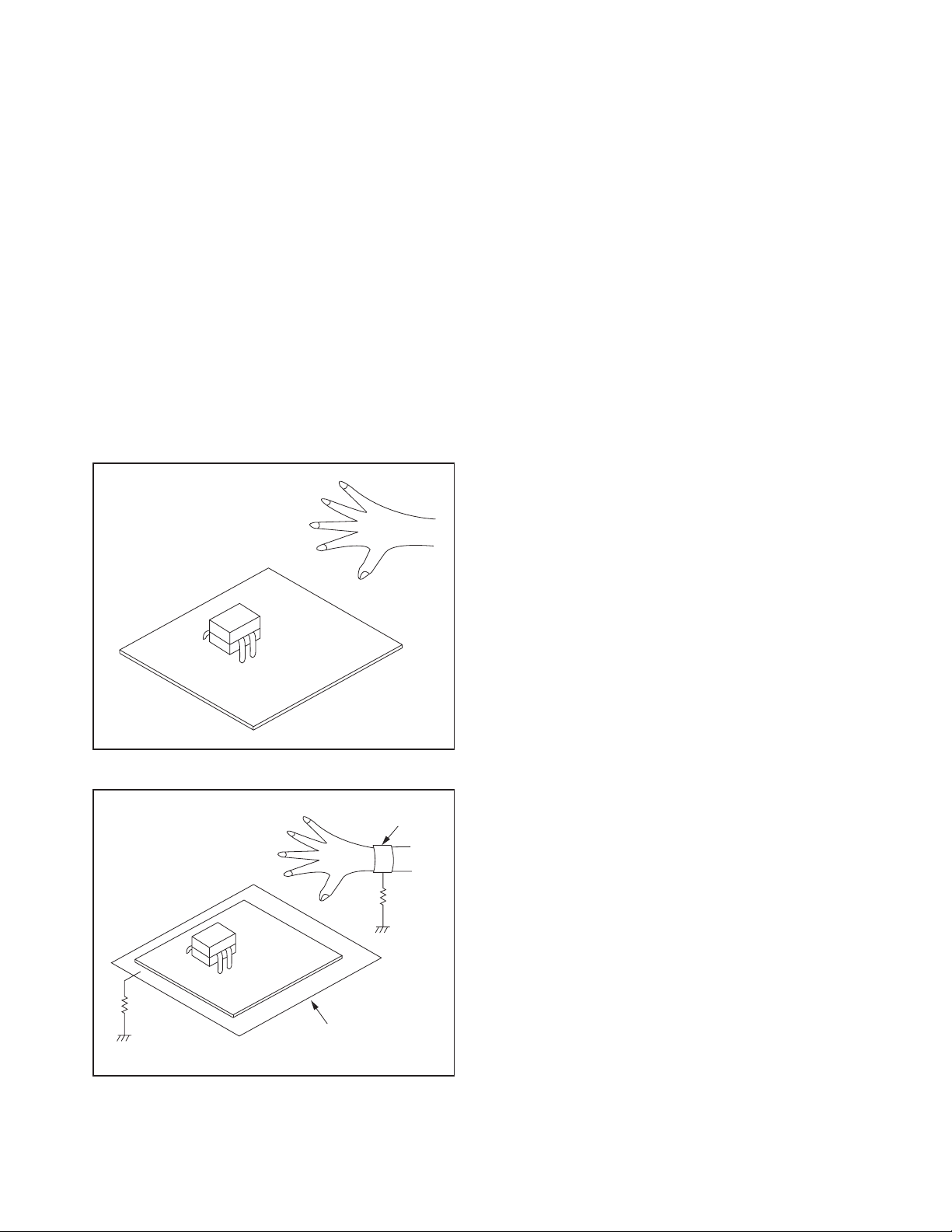
2. Lift each lead of the flat pack-IC upward one by
one, using a sharp pin or wire to which solder will
not adhere (iron wire). When heating the pins, use
a fine tip soldering iron or a hot air desoldering
machine. (Fig. S-1-4)
Sharp
Pin
Fine Tip
Soldering Iron
3. Bottom of the flat pack-IC is fixed with glue to the
CBA; when removing entire flat pack-IC, first apply
soldering iron to center of the flat pack-IC and heat
up. Then remove (glue will be melted). (Fig. S-1-6)
4. Release the flat pack-IC from the CBA using
tweezers. (Fig. S-1-6)
Fig. S-1-4
1-4-2 BDN_SN
Page 9
With Iron Wire:
1. Using desoldering braid, remove the solder from
all pins of the flat pack-IC. When you use solder
flux which is applied to all pins of the flat pack-IC,
you can remove it easily. (Fig. S-1-3)
2. Affix the wire to a workbench or solid mounting
point, as shown in Fig. S-1-5.
3. While heating the pins using a fine tip soldering
iron or hot air blower, pull up the wire as the solder
melts so as to lift the IC leads from the CBA
contact pads as shown in Fig. S-1-5.
4. Bottom of the flat pack-IC is fixed with glue to the
CBA; when removing entire flat pack-IC, first apply
soldering iron to center of the flat pack-IC and heat
up. Then remove (glue will be melted). (Fig. S-1-6)
5. Release the flat pack-IC from the CBA using
tweezers. (Fig. S-1-6)
Note: When using a soldering iron, care must be
taken to ensure that the flat pack-IC is not
being held by glue. When the flat pack-IC is
removed from the CBA, handle it gently
because it may be damaged if force is applied.
Hot Air Blower
2. Installation
1. Using desoldering braid, remove the solder from
the foil of each pin of the flat pack-IC on the CBA
so you can install a replacement flat pack-IC more
easily.
2. The “ I ” mark on the flat pack-IC indicates pin 1.
(See Fig. S-1-7.) Be sure this mark matches the
pin 1 on the PCB when positioning for installation.
Then presolder the four corners of the flat pack-IC.
(See Fig. S-1-8.)
3. Solder all pins of the flat pack-IC. Be sure that
none of the pins have solder bridges.
Example :
Pin 1 of the Flat Pack-IC
is indicated by a " " mark.
Fig. S-1-7
To Solid
Mounting Point
CBA
Tweezers
Iron Wire
Soldering Iron
Fig. S-1-5
Fine Tip
Soldering Iron
Flat Pack-IC
or
Presolder
Flat Pack-IC
CBA
Fig. S-1-8
Fig. S-1-6
1-4-3 BDN_SN
Page 10
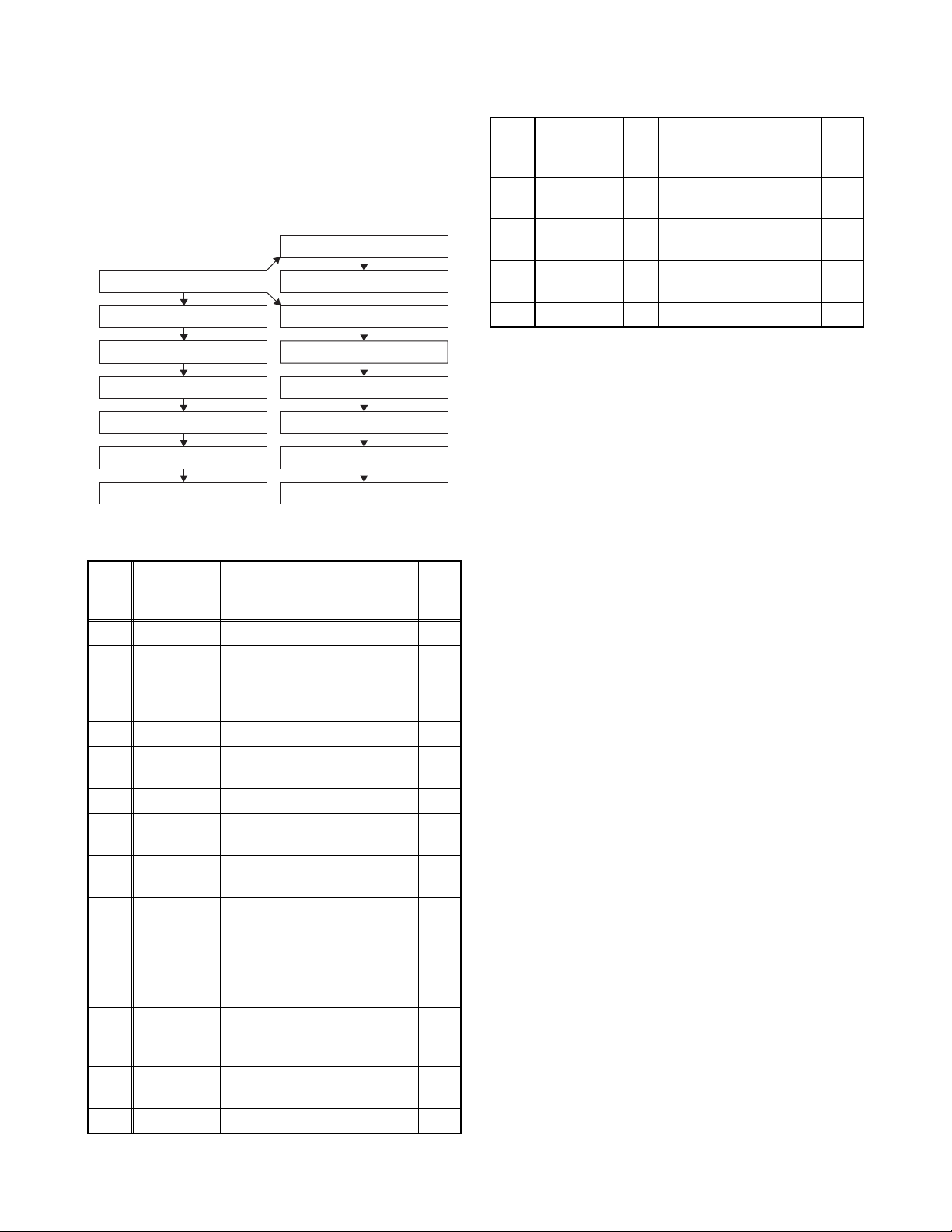
Instructions for Handling Semiconductors
Electrostatic breakdown of the semi-conductors may
occur due to a potential difference caused by
electrostatic charge during unpacking or repair work.
1. Ground for Human Body
Be sure to wear a grounding band (1 MΩ) that is
properly grounded to remove any static electricity that
may be charged on the body.
2. Ground for Workbench
Be sure to place a conductive sheet or copper plate
with proper grounding (1 MΩ) on the workbench or
other surface, where the semi-conductors are to be
placed. Because the static electricity charge on
clothing will not escape through the body grounding
band, be careful to avoid contacting semi-conductors
with your clothing.
<Incorrect>
<Correct>
1MΩ
CBA
Grounding Band
1MΩ
CBA
Conductive Sheet or
Copper Plate
1-4-4 BDN_SN
Page 11
CABINET DISASSEMBLY INSTRUCTIONS
1. Disassembly Flowchart
This flowchart indicates the disassembly steps to gain
access to items to be serviced. When reassembling,
follow the steps in reverse order. Bend, route, and
dress the cables as they were originally.
[10] Fan Cover
[1] Top Cover
[8] BD Main CBA
[9] BD Mechanism Assembly
[12] AV CBA
[13] AMP/PSU CBA
[14] SD Card CBA
[15] MP3 CBA
[11] Rear Panel
[2] Front Unit
[3] Front CBA
[4] Power SW CBA
[5] WiFi CBA
[6] Rotary CBA
[7] Front Assembly
2. Disassembly Method
ID/
Loc.
No.
[1] Top Cover D1 8(S-1) ---
[2] Front Unit D2
[3] Front CBA D2 --------------- ---
[4]
[5] WiFi CBA D3 --------------- ---
[6]
[7]
[8]
[9]
[10] Fan Cover D6
[11] Rear Panel D6 3(S-8), (S-9), 2(S-10) 3
Part
Power SW
CBA
Rotary
CBA
Front
Assembly
BD Main
CBA
BD
Mechanism
Assembly
Fig.
No.
D3 2(S-3) ---
D4
D4 --------------- ---
D5
D5 4(S-6) 2
Removal
5(L-1), 3(L-2), 3(L-3),
4(S-2), CN2005,
CN2006, CN2007,
CN7601
Volume Knob, Nut,
Washer
(S-4), 2(S-5), CN101,
CN301, CN302,
CN6101, CN7001,
CN7101, M-PCB Plate
Earth, Locking Card
Spacer
(S-7), CN5001,
Fan Earth Plate
Note
1
---
2
---
ID/
Loc.
No.
[12] AV CBA D7
[13]
[14]
[15] MP3 CBA D8 (S-14) ---
↓
(1)
Note:
(1) Identification (location) No. of parts in the figures
(2) Name of the part
(3) Figure Number for reference
(4) Identification of parts to be removed, unhooked,
unlocked, released, unplugged, unclamped, or
desoldered.
P = Spring, L = Locking Tab, S = Screw,
CN = Connector
e.g. 2(S-2) = two Screws of (S-2),
2(L-2) = two Locking Tabs of (L-2)
(5) Refer to “Reference Notes.”
Part
AMP/PSU
CBA
SD Card
CBA
↓
(2)
Fig.
No.
D7
D8 2(S-13) ---
↓
(3)
Removal
2(S-11), CN402,
CN403
5(S-12), CN9002,
PCB Bracket Front
↓
(4)
Note
---
---
↓
(5)
Reference Notes
1. CAUTION 1: Locking Tabs (L-1), (L-2) and (L-3)
are fragile. Be careful not to break them.
2. When replacing the BD Mechanism Assembly
or BD Main CBA, refer to "ADJUSTMENT
INSTRUCTIONS FOR BD MAIN CBA OR BD
MECHANISM ASSEMBLY REPLACEMENT."
3. When reassembling, be sure to use the original
screws or specified screws listed in the parts
list.
1-5-1 EDA02DC
Page 12
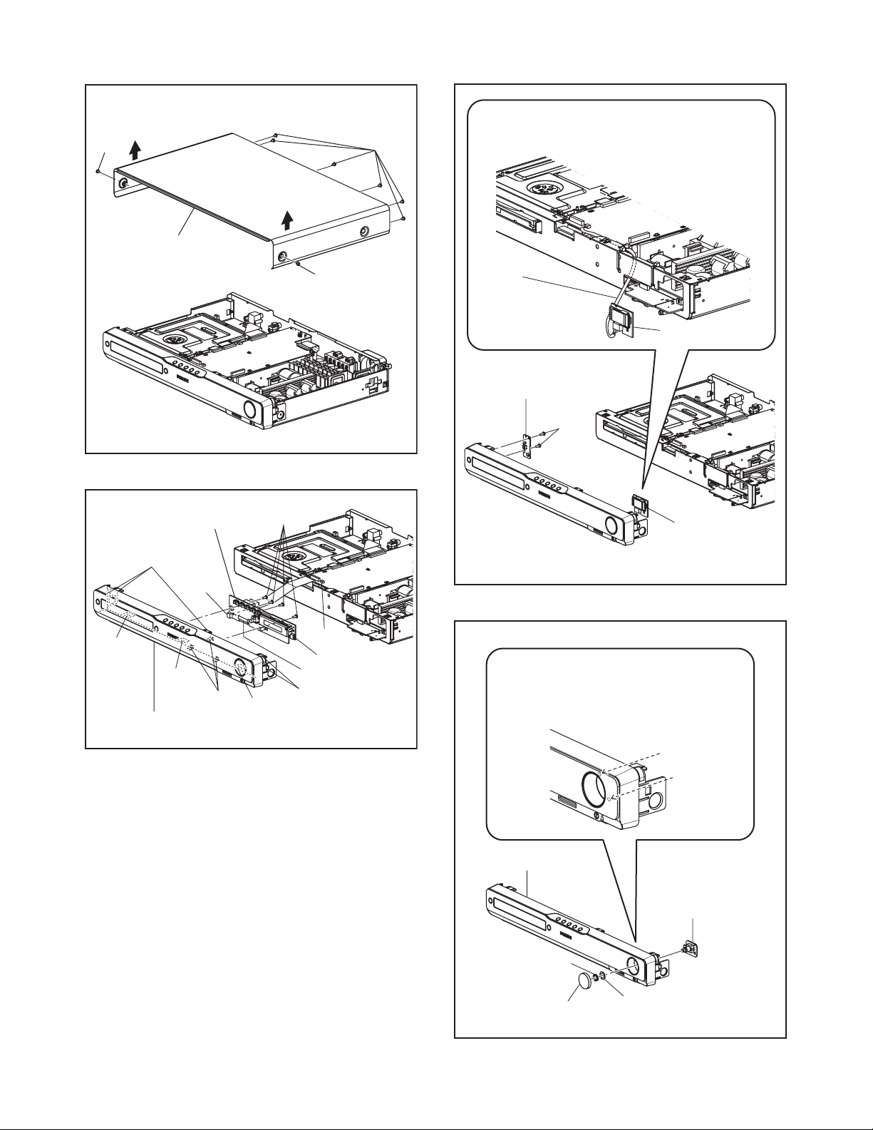
(S-1)
[1] Top Cover
(S-1)
The cable (connected to the WiFi
CBA) should be placed as shown.
[3] Front CBA
(L-1)
(L-2)
(L-2)
[2] Front Unit
CN2006
(L-3)
(L-2)
(S-2)
(S-1)
CN7601
CN2007
CN2005
(L-1)
Cable
(connected to
the WiFi CBA)
WiFi CBA
[4] Power SW CBA
(S-3)
Fig. D1
[5] WiFi CBA
Fig. D3
From behind the front panel,
push the two holes with a driver
or hexagonal wrench to remove
the volume knob.
Fig. D2
[7] Front Assembly
[6] Rotary CBA
Nut
Volume Knob
Washer
Fig. D4
1-5-2 EDA02DC
Page 13
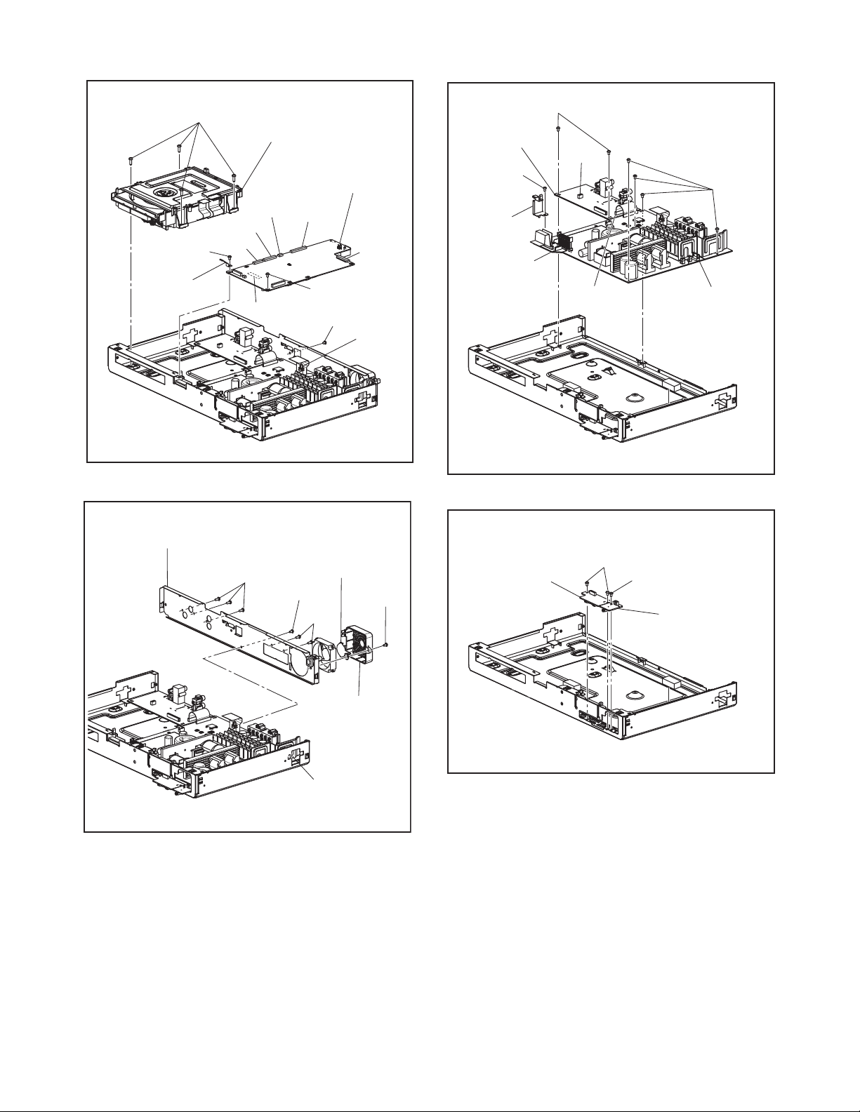
(S-6)
[9] *BD Mechanism
Assembly
[8] *BD Main CBA
[12] AV CBA
(S-12)
(S-11)
CN402
(S-12)
CN101
CN302
(S-5)
M-PCB
Plate
Earth
CN6101
* See Reference Note 2.
[11] *Rear Panel
(S-8)
CN301
CN7101
(S-5)
(S-4)
Fan Earth Plate
(S-9)
(S-10)
CN7001
Locking
Card
Spacer
Fig. D5
(S-7)
PCB Bracket
Front
CN9002
[14] SD Card CBA
CN403
(S-13)
[13] AMP/PSU
CBA
Fig. D7
(S-14)
[15] MP3 CBA
* See Reference Note 3.
[10] Fan Cover
Fig. D8
CN5001
Fig. D6
1-5-3 EDA02DC
Page 14
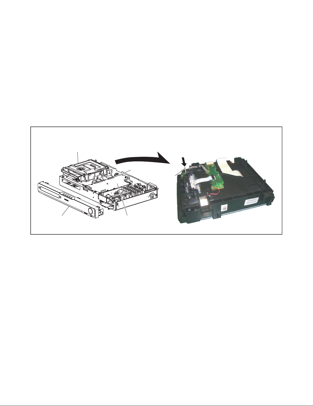
3. How to Eject a Disc
When a disc cannot be removed due to malfunction or when an unplayable disc is inserted, follow the
procedure below to remove the disc.
Procedure A
1. Unplug the AC power cord and then plug it in.
2. Turn the power on by pressing the [ A] button and the disc tray will open automatically.
Procedure B
1. Remove the Top Cover and Front Unit.
2. Disconnect connector (CN7101) on the BD Main CBA.
3. Remove the BD Mechanism Assembly.
4. Slide the portion A in the direction of the arrow from bottom side of the BD Mechanism Assembly.
5. Pull the tray out manually and remove the disc.
BD Mechanism Assembly
Front Unit
Bottom of BD Mechanism Assembly
CN7101
Portion A
BD Main CBA
1-5-4 EDA02DC
Page 15

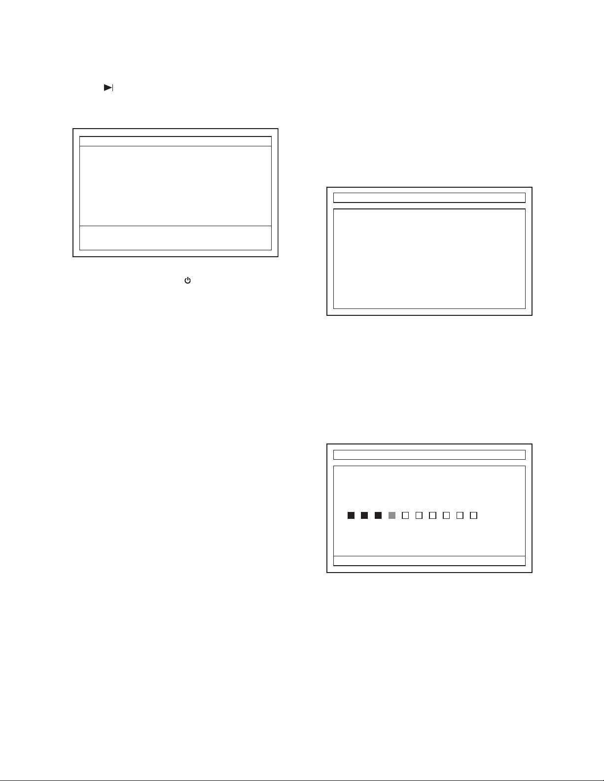
HOW TO INITIALIZE THE BLU-RAY DISC HOME THEATER
To put the program back at the factory-default,
initialize the BD player as the following procedure.
Note:
• By initializing, network is reset to disconnected state
and “Network Service Disclaimer” appears on the
screen.
• Once the unit is initialized, the unit starts in Virgin
Mode the next time it is turned on. The Virgin Mode
allows quick set up of language and network settings.
To exit this mode, select “Cancel” on the screen.
1. Turn the power on.
2. Remove the disc on the tray and close the tray.
3. Press [ ] (skip up), [1], [2], and [3] buttons on the
remote control unit in this order.
Fig. a appears on the screen. All VFD lights.
"*" differ depending on the models.
Version Display
F/W Name
Version
Region
Pickup
ESN
DRM
: *******
: *.**.**
: *-*
: **
: ********************************
: OK
Default Setting : --
Default Setting : STOP End : STANDBY-ON
VFD/LED Check : OK
Fig. a
4. Press [ C ] button on the remote control unit.
Fig. b appears on the screen and Fig. c appears
on the VFD.
"*" differ depending on the models.
Version Display
F/W Name
Version
Region
Pickup
ESN
DRM
Default Setting : SUCCESS
Default Setting : STOP End : STANDBY-ON
VFD/LED Check : OK
: *******
: *.**.**
: *-*
: **
: ********************************
: OK
Fig. b
Fig. c
5. After initializing, the power will turn off
automatically.
1-6-1 E1U21INT
Page 16
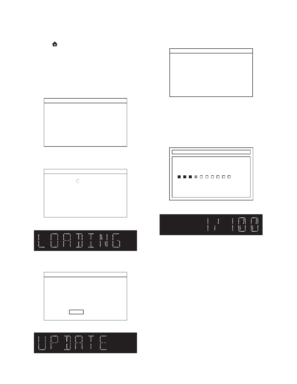
FIRMWARE RENEWAL MODE
Note:
The file extension of the available firmware is “b41”.
1. Turn the power on and remove the disc on the tray
and close the tray.
2. Press [ ] (skip up), [6], [5], and [4] buttons on the
remote control unit in this order.
Fig. a appears on the screen.
"*" differ depending on the models.
F/W Version Mode
Please select software update mode.
Disc
USB
SD Card
The available software update mode will
differ depending on the model type.
F/W Name : ******* Ver *.**.**
Fig. a Version Up Mode Screen (Example)
3. Select “Disc” or “USB” or “SD Card” and press
[OK] button on the remote control unit. The tray
will open automatically, if “Disc” is selected.
4. Insert the disc or USB Memory Stick or SD Card
for version up.
5. The BD player enters the F/W version up mode
automatically. Fig. b will appear on the screen.
Make sure to insert the proper F/W for the state of
this model.
"*" differ depending on the models.
F/W Version Mode
F/W Name : ******* Ver *.**.**
6. After reading the new firmware, the power will turn
off automatically.
7. The power turns on and updating starts
automatically.
Fig. c will appear on the screen.
Software Update
Please wait for a few minutes. Do not unplug the AC cord or interrupt the
updating process. When update is completed unit will automatically turn off,
and unit will automatically turn back on.
Updating Software....
******* Ver *.**.**
CHECK SUM : - - - -
"*" differ depending on the models.
Fig. c Version Up Mode
8. After the update, Fig. d will appear on the VFD and
the power will turn off automatically.
Fig. d
VFD upon Finishing the Programming Mode (Example)
9. The power turns back on automatically. If disc
mode was selected, the tray will open
automatically. Remove the disc or USB Memory
Stick or SD Card from the unit.
Notes:
• All the settings will be put back to factory-default.
• Do not unplug the AC cord and do not remove the
disc or USB Memory Stick or SD Card while this
procedure.
(*1)
Loading Disc...
Fig. b Programming Mode Screen (Example)
The appearance shown in (*1) of Fig. b is
described as follows:
No. Appearance State
1 Loading Disc... Loading the disc
Checking the new
2 Reading...
firmware and preparing
the update system
Updating
3
Software...
Downloading and
writing the new firmware
The following USB Memory Stick/SD Card can be
used for software update. Make sure to use a device
that has enough space.
• USB Memory Stick (FAT16/FAT32 file system)
•
SD/Mini SD/Micro SD Card (FAT12/FAT16 file system)
•
SDHC/Mini SDHC/Micro SDHC Card (FAT32 file system)
1-7-1 HT3.5(P&F)_(VFD)FW
Page 17
How to Verify the Firmware Version
1. Turn the power on.
2. Remove the disc on the tray and close the tray.
3. Press [ ] (skip up), [1], [2], and [3] buttons on the
remote control unit in this order.
Fig. e appears on the screen. All VFD lights.
"*" differ depending on the models.
Version Display
F/W Name
Version
Region
Pickup
ESN
DRM
: *******
: *.**.**
: *-*
: **
: ********************************
: OK
When update is interrupted during
the Software Update
In a case where software update is interrupted due to
unplugging of AC cord, removal of SD card or power
outage, the unit will start from the software update
mode the next time it is turned on. (Unless the update
is completed, the unit starts from software update
mode and not from the Home Menu.)
Fig. f appears on the screen when software update is
interrupted.
Software Update
Default Setting : --
Default Setting : STOP End : STANDBY-ON
VFD/LED Check : OK
Fig. e
4. To exit this mode, press [ ] button.
The software update failed. For the state that the remote control key does not
work, press the [STANDBY/ON] key of this unit for 10 seconds. As this unit will
turn off, press the [STANDBY/ON] key again. After this unit turns back on, the
software update will start again.
If the software update failed with above procedure, please do the following.
1. Write the software downloaded on our website in SD Memory Card.
2. Press the [STANDBY/ON] key of this unit for 10 seconds.
3. As this unit will turn off, press the [STANDBY/ON] key.
Fig. f
Follow the procedures below to enter the software
update mode again.
1. Press the [STANDBY/ON] button of this unit for 10
seconds.
2. As this unit will turn off, press the [STANDBY/ON]
button again.
3. After this unit turns back on, the software update
will start again. Fig. g will appear.
Software Update
Please wait for a few minutes. Do not unplug the AC cord or interrupt the
updating process. When update is completed unit will automatically turn off,
and unit will automatically turn back on.
Updating Software....
******* Ver *.**.**
CHECK SUM : - - - -
"*" differ depending on the models.
Fig. g
Note:
If the software update fails following the above
procedure, please perform the following.
1. Write the software downloaded on our website in
SD Memory Card.
2. Insert the SD Memory Card into the SD card slot.
3. Press the [STANDBY/ON] button of this unit for 10
seconds.
4. As this unit will turn off, press the [STANDBY/ON]
button.
1-7-2 HT3.5(P&F)_(VFD)FW
Page 18
FIRMWARE RENEWAL MODE (for User)
Disc/USB Memory Stick/SD Card Update
1. Press [ ] button to display Setup menu.
2. Select Setup - Advanced Setup - Software Update.
3. Select the software update mode from "Disc" or
“USB” or “SD Card.” The available software update
mode will differ depending on the model type.
4. The screen appears in Fig. h when “Yes” is
chosen. If disc mode was selected, the tray will
open automatically.
Insert the disc or USB Memory Stick or SD Card for
software update.
Please insert a disc for software update. If you want to exit update,
press [BACK].
Software Update
7. Fig. m will appear on the screen.
8. After a few minutes, the power will turn off
9. The power turns on and updating starts
Software Update
Please wait for a few minutes. During the updated process the player
will automatically turn off and turn back on.
Fig. m
automatically.
automatically.
Fig. n will appear on the screen and update
progress will be displayed as shown in Fig. o on
the VFD.
Fig. h (Example of Disc mode)
5. Disc loading starts. Fig. i will appear on the screen
and Fig. j will appear on the VFD.
Software Update
Loading Disc....
Fig. i (Example of Disc mode)
Fig. j VFD in Update Mode
6. Fig. k will appear on the screen, then select “Yes”.
Fig. l will appear on the VFD.
Software Update
Current Version : X.XX.XX
: X.XX.XXInsert Version
Software Update
Please wait for a few minutes. Do not unplug the AC cord or interrupt the
updating process. When update is completed unit will automatically turn off,
and unit will automatically turn back on.
Updating Software....
Fig. n
Fig. o VFD in Update Mode
10. After the update, the power turns off and then
turns back on automatically. If disc mode was
selected, the tray will open automatically. Remove
the disc or USB Memory Stick or SD Card from the
unit.
Note: The setup setting configured before the update
will be kept.
Select 'Yes' and press [OK] button start updating. Press 'No' to exit
software update.
No Yes
Fig. k
Fig. l VFD in Update Mode
The following USB Memory Stick/SD Card can be
used for software update. Make sure to use a device
that has enough space.
• USB Memory Stick (FAT16/FAT32 file system)
• SD/Mini SD/Micro SD Card (FAT12/FAT16 file
system)
• SDHC/Mini SDHC/Micro SDHC Card (FAT32 file
system)
1-7-3 HT3.5(P&F)_(VFD)FW
Page 19

Network Update
1. Press [ ] button to display Setup menu.
2. Select Setup - Advanced Setup - Software Update
- Network.
3.
When “Yes” is chosen, the screen appears in Fig. p
and the unit starts connecting to the network.
Software Update
Network Connecting...
7. The power turns on and updating starts
automatically.
Fig. s will appear on the screen and Fig. t will
appear on the VFD.
Software Update
Please wait for a few minutes. Do not unplug the AC cord or interrupt the
updating process. When update is completed unit will automatically turn off,
and unit will automatically turn back on.
Updating Software....
Fig. p
4. The firmware version confirmation screen (Fig. q)
will appear on the screen. Select “Yes” and press
[OK] button.
Software Update
Current Version : X.XX.XX
The latest software can be download. Do you want to download?
: X.XX.XXInsert Version
No Yes
Fig. q
5. Fig. r will appear on the screen.
Software Update
Please wait for a few minutes. During the updated process the player
will automatically turn off and turn back on.
Fig. s
Fig. t
8. After the update, the power turns off and then
turns back on automatically.
Note: The setup setting configured before the update
will be kept.
Network Error Message
No. Error Message
The cable is not connected.
1
Please confirm the connection of the cable.
DHCP cannot be acquired.
2
Please confirm connection or set it with the
manual operation.
Internet Protocol address is not set.
3
Please confirm the set content.
Fig. r
6. After a few minutes, the power will turn off
automatically.
The equipment with same Internet Protocol
4
address already exists.
Please set another Internet Protocol address.
There is no response from Default gateway.
5
Please confirm the address of Default
gateway.
It is not possible to connect to the DNS server.
6
Please confirm the Internet connection or the
DNS address setting.
It is not possible to connect to the server.
7
Please contact our support center.
It is not possible to confirm the software
8
version.
Please contact our support center.
Cannot connect to the wireless network.
9
Please confirm the wireless network setting.
1-7-4 HT3.5(P&F)_(VFD)FW
Page 20

ADJUSTMENT INSTRUCTIONS FOR BD MAIN CBA OR
BD MECHANISM ASSEMBLY REPLACEMENT
When replacing either BD Main CBA or BD Mechanism Assembly, the unique OPU DATA of the BD Mechanism
needs to be written into the BD Main CBA. Follow the procedure below for OPU DATA write operation.
Equipments:
• PC (OS: Windows XP strongly recommended)
• Barcode reader
• COMTOOL jig relay board + 6PIN FFC cable
• USB cable Type AB
• Device driver for COMTOOL jig (CDM 2.06.00 WHQL Certified)
• Specialized application (OpuDataWriter)
Caution:
Always turn the unit power off before connecting the FFC cable or removing the FFC cable from the BD Main CBA
•
1. Preparation Of Work Environment
1-1.
For the OPU DATA write operation, refer to the connection diagram and connect each device as shown below.
Connection Diagram
Note: The unit configuration may differ depending on model types.
.
Unit (Completed product)
BD Mechanism
Assembly
BD Main CBA
Connect to 6-pin connector
of BD Main CBA
6-pin FFC cable
6-pin
connector
USB cable Type AB
(To USB Port)
COMTOOL Jig Relay Board
PC
Barcode Reader
(To USB Port)
Location of Pin 1 on COMTOOL Jig Relay Board
Lower side of Ref. No CN06 is pin 1 (printed 1 by silk)
1-8-1 HT3.5(2D)_HT_AIR
Page 21

Caution:
• Make sure the FFC cable is inserted in the proper direction so the Pin 1 of COMTOOL jig relay board and Pin 1
of BD MAIN CBA connector is connected.
Location of Pin 1 on BD Main CBA
1pin
Pin 1 is located on the left side
• If the device driver (CDM 2.06.00 WHQL Certified) of COMTOOL jig relay board is not installed in the PC, install
this before connecting COMTOOL jig relay board to the PC.
<How to install the device driver for COMTOOL jig relay board>
1) Save the device driver for COMTOOL jig relay board in the C: drive.
2) Connect COMTOOL jig relay board to the PC.
3) The driver installation screen opens. Select [Install from a list or specific location (Advanced)] then click
[Next].
4) Select [Search for the best driver in these locations.] then check the box for [Include this location in the
search:].
5) Click on Browse button then select the device driver (CDM 2.06.00 WHQL Certified) folder in the C: drive.
Click [Next].
6) Confirm that installation of [USB Serial Converter] device driver has completed and click on [Finish].
2. How To Check Which Port Is Used For COMTOOL Jig Relay Board
2-1. Click on the Windows [Start] button on the PC.
2-2. Right click on [My Computer].
2-3. Click on [Properties].
2-4. Click on [Hardware] tab in System Properties window.
2-5. Click on [Device Manager].
2-6. Click on [Ports (COM&LPT)].
2-7. Check which connection port is assigned for [USB Serial Port] (e.g. COM1).
The connection port number assigned here will be used later during setup of application.
3. Application Setup
3-1. Save the application folder (OpuDataWriter) directly under the C: drive.
3-2. Create a shortcut for [OpuDataWriter.exe] which is located inside the folder on the desktop.
1-8-2 HT3.5(2D)_HT_AIR
Page 22

4. OPU DATA WRITE
4-1. Connect the unit’s AC power cord. Wait for about 30 seconds until the unit is in standby mode.
4-2. Double click on the [OpuDataWriter.exe] shortcut on the desktop to start the application.
4-3. Application start screen appears.
Select the assigned connection port of [USB Serial Port] for the [COM PORT] field located at the right corner
of the screen.
Check that [Please input OPU DATA] message is displayed in the Status Display.
Set the cursor position at the blank box next to the [OPU DATA].
Cursor position
Status Display
Select the assigned COM PORT
4-4. Using the Barcode reader, scan the QR code attached on the side of the BD Mechanism Assembly.
QR Code
4-5. Check that [FE CONNECTION CHECK] message appears on the Status Display then turn the unit power on.
Status Display
If error occurs:
If an error occurs, the screen changes to a red display. In such case, close the window and then unplug the
unit AC power cord. Check if each device is properly connected then repeat from step 1.
1-8-3 HT3.5(2D)_HT_AIR
Page 23

4-6. Data write begins. While writing data, the Status Display message will change.
SEND LD PAR
Status Display
4-7. [OK] appears in the Status Display if data write has been completed successfully.
If error occurs:
• If an error occurs, the screen changes to a red display. In such case, close the window and then unplug the
unit AC power cord. Check if each device is properly connected then repeat from step 1.
• If an error other than connection error occurs for more than 3 times, the BD MAIN CBA or BD Mechanism
Assembly may be defected. Replace with a new one before performing the OPU DATA write.
4-8. After data write has been completed successfully, unplug the AC power cord.
4-9. Remove the FFC Cable of COMTOOL jig relay board connected to the BD Main CBA.
Then disconnect all devices connected to the unit.
1-8-4 HT3.5(2D)_HT_AIR
Page 24

Error Code
Error Code Error Description
10 Start word error The first letter entered for [LOADER S/N] does not match.
101 [ReadBackup]Drive Mount error Cannot mount the drive set for [ReadBackup] folder.
102 [Transfer]Drive Mount error Cannot mount the drive set for [Transfer] folder.
103 [OpuData]Drive Mount error Cannot mount the drive set for [OpuData] folder.
104 [Log]Drive Mount error Cannot mount the drive set for [Log] folder.
210 Start word error The first letter entered for [OPU DATA] does not match.
300 CheckSum NG
301 QRCheckSum NG [Process1]CheckSum Test error.
310 CreateHeader NG [Process2]Error creating Header region.
320 CreateLDD NG [Process3]Error creating LDD region.
330 CreateFBIAS NG [Process4]Error creating FBIAS region.
340 CreateExp NG [Process5]Error creating EXP region.
350 CreateLcd NG [Process6]Error creating LCD region.
360 CreateCrc NG [Process7]Error creating CRC region.
370 CreateDDD NG [Process8]Error creating DDD file.
380 CreateLog NG [Process9]Error creating LOG file.
390 CreateOpuData NG [Process10]Error creating OPU DATA file.
1010 Start word error The first letter entered for [LOADER S/N] does not match.
1130 DDDFile not found
1140 DDDFile search error Error occurred while searching DDD file in [WriteBackup] folder.
1151 [WriteBackup]Drive Mount error Cannot mount the drive set for [WriteBackup] folder.
1152 [Transfer]Drive Mount error Cannot mount the drive set for [Transfer] folder.
1153 [OpuData]Drive Mount error Cannot mount the drive set for [OpuData] folder.
1154 [Log]Drive Mount error Cannot mount the drive set for [Log] folder.
1210 ComConnection TIME OUT
1211 Tray Close error Cannot close tray.
1220 TestUnitReady ERROR0 [ERROR0] returned for TestUnitReady command issued.
1221 TestUnitReady ERROR1 [ERROR1] returned for TestUnitReady command issued.
1222 TestUnitReady TIME OUT No reply received for TestUnitReady command issued.
1230 ReadVirRAM32 NG
1240 WriteReg16 NG
1250 WriteReg1 NG
1260 FlashWrite ERROR0 [ERROR] returned for FlashWrite command issued.
1261 FlashWrite ERROR1 [ERROR] returned for FlashWrite command issued.
1262 FlashWrite TIME OUT No reply received for FlashWrite command issued.
1310 MoveDDDFile NG [Move DDD file to written folder]Process Error
1320 CreateLog NG [Create LOG file]Process Error
1330 CreateComLOG NG [COM PORT connection LOG file create]Process Error
1400 TIME OUT System Time Out
2031 LdParamSend NG LD Parameter Send Error
The checksum of the entered OPU DATA(QR code) does not
match.
As a result of searching DDD file in the [WriteBackup] folder, the
entered DDD file for [LOADER S/N] could not be found.
No reply received for NOP commmand (20 times at 500mSec
interval).
[Acquire DRAM head address of DDD data forwarding
region]Process Error
[Send ddd data to DRAM head address region(16BYTE unit)]
Process Error
[Send ddd data to DRAM head address region(1BYTE
unit)]Process Error
1-8-5 HT3.5(2D)_HT_AIR
Page 25

Error Code Error Description
2042 LdParamClear ERROR0 Cannot initialize LD Parameter.
2043 LdParamClear ERROR1 Cannot initialize LD Parameter.
2044 LdParamClear TIME OUT Cannot initialize LD Parameter (TimeOut).
2051 IopSet NG Iop Set Error
2052 IopSet ERROR0 Iop Set Error
2053 IopSet ERROR1 Iop Set Error
2054 IopSet TIME OUT lop Set Error (TimeOut)
2055 IopSet ERROR0 Iop Set Error
2056 IopSet ERROR1 Iop Set Error
2057 IopSet TIME OUT lop Set Error (TimeOut)
2058 CD Iop LIMIT NG CD Iop exceeds limit value.
2059 DVD Iop LIMIT NG DVD Iop exceeds limit value.
2060 BD Iop LIMIT NG BD Iop exceeds limit value.
2081 LdParamVerify NG LD Parameter Verify Error
2091 AtapiComCheck NG BE start Error.
2101 ID4 OFF NG Cannot set ID4 OFF.
2111 SET BOR RATE NG Failed to change Serial Connection Rate.
2200 Genaration NG Generation detect failure.
6001 Factory Info save Error Failed to create FactoryInfo file.
6002 Factory Info save Error Failed to create FactoryInfo file.
6100 Factory Info save Error Failed to create FactoryInfo file.
5. Saving The Pre-Operation OPU DATA
OPU DATA before performing the OPU DATA write is saved in a folder automatically.
5-1. When the OPU DATA write operation has been completed successfully, a folder named [FactoryInfo] is
created in the application folder (OpuDataWriter).
5-2. In the [FactoryInfo] folder, a folder is created monthly in which text file data are saved.
This text file is created with a file name of the OPU serial number and contains the pre-operation OPU DATA.
Pre-operation OPU DATA text file
Year(2010)Month(12)
5-3. The text file is necessary for analyzing the defective BD Mechanism. Submit this text file with the defective
BD Mechanism as necessary to the appropriate managing Department.
1-8-6 HT3.5(2D)_HT_AIR
Page 26

FLOW CHART NO.1
The power cannot be turned on.
TROUBLESHOOTING
Is the fuse normal?
Ye s
Is normal state restored when once unplugged
power cord is plugged again after several seconds.
Ye s
Is 3.5V voltage outputted to the cathode of D9024?
Ye s
Are the voltage of each pin of CN9001 become
as shown below?
CN9001
CN9001
CN9001
CN9001
CN9001
CN9001
Check each rectifying circuit of secondary circuit
and replace BD Main CBA if defective.
FLOW CHART NO.2
The fuse blows out.
1-3PIN
4,6PIN
9,11,13PIN
10PIN
19,20PIN
22PIN
+1.8V
+5V
+1.2V
+10.5V
+3.3V
+5V
Ye s
1V8
5V-1, U5V
1V2
10V5
3V3
5V-2
No
No
No
No
See FLOW CHART No.2 <The fuse blows out.>
Check for leak or short-circuiting of primary
circuit component and replace AMP/PSU CBA
if defective.
Replace AMP/PSU CBA.
Check the presence that the primary component
is leaking or shorted and replace AMP/PSU CBA
if defective.
After servicing, replace the fuse (F9000).
FLOW CHART NO.3
Picture does not appear normally.
Set the disc on the disc tray, and playback.
(Composite output)(HDMI output)
Are the video signals outputted to Pin(23) of
CN404?
Ye s
Replace AV CBA.
Replace BD Main CBA or BD MECHANISM
ASSEMBLY.
Check the presence that the rectifying diode or circuit
is shorted in each rectifying circuit of secondary side
and replace AMP/PSU CBA if defective.
No
Replace BD Main CBA or BD MECHANISM
ASSEMBLY.
1-9-1 E1U00TR
Page 27

FLOW CHART NO.4
Audio does not appear normally.
Set the disc on the disc tray, and playback.
Ye s
Are the audio signals(serial data) outputted to
Pin(3, 4, 5, 6) of CN201?
Ye s
Replace AMP/PSU CBA.
No
Replace BD Main CBA or BD MECHANISM
ASSEMBLY.
1-9-2 E1U00TR
Page 28

ERROR MESSAGE
Note: Only error messages for the unit’s corresponding media will appear.
Playback feature may not be available on this Disc.
Error Message
Disc Error
Loader Error
Parental Lock Error
Region Error
The device connected for HDMI
connection does not support HDCP.
- - Please eject the disc. - -
Disc Error
Disc Error
- - Please eject the disc. - Playback feature may not be available on this Disc.
Loader Error
The unit stopped automatically due to loader error.
Please open the disc tray once and then close it.
Parental Lock On
The current selected parental level prohibits playback.
Region Error
Playback is not authorized in your region.
Region code of this disc :
(There is no message.)
The following error will appear on the VFD.
USB/SD Card Error
BD-Live Network Connecting Error
LAN Cable Not Connected
Cannot Acquire DHCP Server
Cannot Acquire IP Address
Already Existing IP Address
No Response From Default
Gateway
Cannot Connect To DNS Server
Memory Device Error
- - Please check the Memory Device. - There is no playback file on the Memory Device or Device has incorrect/
no format.
BD-Live Setting Error
Network connection is interrupted. Please confirm “BD-Live Setting”.
The cable is not connected.
Please confirm the connection of the cable.
DHCP cannot be acquired.
Please confirm connection or set it with the manual operation.
Internet Protocol address is not set.
Please confirm the set content.
The equipment with same Internet Protocol address already exists.
Please set another Internet Protocol address.
There is no response from Default gateway.
Please confirm the address of Default gateway.
It is not possible to connect to the DNS server.
Please confirm the Internet connection or the DNS address setting.
1-10-1 E1U00ER
Page 29

Error Message
Cannot Connect To Server
Cannot Confirm Firmware Version
Firmware Update Error
(Update File Error)
Cannot Connect To Download
Server
Cannot connect to wireless
network.
USB Error
It is not possible to connect to the server.
Please contact our support center.
It is not possible to confirm the software version.
Please contact our support center.
Error detected.
File may be corrupted.
Please download software again.
Error detected.
Please confirm whether it is SD Memory Card that corresponds to
software update.
Error detected.
Please confirm whether it is USB device that corresponds to software
update.
It is not possible to connect to the server.
Please contact our support center.
Cannot connect to the wireless network.
Please confirm the wireless network setting.
Error in the USB Connection. USB operation has been stopped
automatically. Please remove the USB device and restart the unit.
1-10-2 E1U00ER
Page 30

OVERALL BLOCK Diagram
JK405
VIDEO
CVBS, Composit Y /Cr/Cb OUT
IC301
VIDEO
Driver
CVBSOUT, CompOUT(Y/Cr/Cb)
JK7501
HDMI 19pin
CEC
HDMI
HotPlug
I2C(DDC)
IC7501
HDMI
Transmitter
IRQ
I2S 4, S PDIF
/RST,MCLK,SCLK,LRCLK
Video CLK(4 80i:27MHz,480p: 54MHz:720p,1 080i:74MHz)
IC6601, 2
DDR2 SDRAM
(Nom:512Mbit X 2)
(FullHD,OSD:1Gbit X 2)
IC6501, 2
DDR2 SDRAM
(1Gbit X 2)
IC6901
NAND FLASH
(Nom:512Mbit,)
(w/NetUpdate,Failsafe:1Gbit)
(w/Netflix:2Gbit)
IC6002
8kBit EEPROM
(NO CONNECTION)
CN7902
50pin
CN7901
40pin
CN804
6pin
CN7903
4pin
CN801,2,3
10pin
SW
/VMute, SD/HD LPF1
PON+5V-BE
PON+3V3-BE,
PON+1V2
SCL, SDA
PON+1V8
SCL, SDA
JK403B
COAX
COAX SPDIF
IC405
IC306,
IC307
AV+5V_1
/VMute, SD/HD LPF
AV CBA
74HCU04
PON+1V8
PON+3V3_BE
D3.3V,
PON+10V5
,
D3.3V
A5V
Buffer AMP
Single SW
IC301
SPM Driver
BD Loader unit
2
ARC SPDI F
SPDIF IN
ARC-SPDI FOUT
PON+5V-BE
VHALF
Spindle
+3.3V
CN404
CN7101 30pin
CN101 45pinCN302 16pin
A8V,
D3.3V,
SW
AV+5V_1
30pin
Ipod-TX, Ipod-RX
/VMute,SDHD
SPDIFIN
CompOUT (Y/Cr/Cb),CVBSOUT
IC6001
BP1A
VREFH
IC302
Motor Driver
CN301 4pin
Pick Up
AVCC
BD OPU
Analog
Audio ADC
MCLK
I2S 4
FM_L
IC402
AMP
Audio
L/R IN
IC7201
LRCLK
SCLK
PON+10V5,
A8V, A5V
CN402A
AUX1
AUX1_L
AUX1_R
IC303, IC304
Multi Plexer
Analog
L/R IN
FM_R
AV+12V, AV-12V
Analog
Audio
L/R IN
CN402
BD MAIN CBA
PON+5V-BE
PON+3V3-BE,
PON+5V-BE
/PDN
SCL, SDA
I2S_DATA0-3
/A-Mute, MCLK, LRCLK, SCLK, RST 2, IRQ
SUB-TX, SUB-RX, MD,MC,MS
SYSRST,RDY
PON+3V3-BE,
PON+1V8, PON+1V 2
MII
/RST
LAN Transceiver
SCL,
SDA
74.25/74.1758MHz (Vpix)
33.864
33.33MHz(PC I)
27MHz (V)
PON+3V3_FE( D3.3V)
A8V
Clock Generator
/33.8688/2 4.576MHz (A)
SD-DAT0-3, SD-WP, SD-CD,
SD-CLK, SD-CMD
USBDP,USBDN
PON+3V3_BE
10V5(PON+10V5)
5V-2(PON+5V_ 2,
PON+5V-BE)
8V Reg.
CN6101 30pin
MP3_L
MP3_R
IC404 AMP
MP3-R
MP3-L
2pin(3pin)
IC6401
25MHz
IC6702
Inductor
3V3(PON+3V3)
U5V(USB+5V)
AV+12V,
InputSel1-3
SingleSW1,2
+3.3V
AV+12V, AV-12V
AV+5V_2AV+5V_2
/VMute, SD/HD LPF
SCL, SDA
CEC
PON+3V3-BE
PON+3V3_BE
27MHz
1V8(PON+1V8)
1V2(PON+1V2)
AV-12V
MII
CN7601 5pin
A5V, AVCC
Inductor
5V-1(PON+5V_ 1
PON+5V-FE)
BLOCK DIAGRAM
JK201 16pin
30pin
CN403
CN7001 27pin
LAN JK6401
,
+3.3V
AV+5V_2
AV-12V
W_SDA,W_SCL
AV+12V
+3.3V
30pin
CN202
Input Sel1-3, SingleSW1-2, SD/HD_LPFSW1, /VMute
AMP/uCOM Block
MCLK
LRCLK
W_SCLK
W_TSD1,3
W_RST , W_IRQ
W_SCLK
W_TSD1,3
SW
CEC
EV+3V3
SAFETY
AV-12V
AV+12V
A+5V
34V
FL+
FL+
IC501
D-AMP
IC204
Buffer
AMP
CEC
IC201
EEPROM
EV+3V3
+3V3
JK5001
FL-
FR+
FR+
FL-
SDOUT2,4
+3.3V
WIRELESS_RST,
W_SDA,W_SCL
CEC IN
CEC OUT
FAN+
CN203
WIRELESS_INT
Speaker OUT X 6ch
FR-
SL+
SL-
SL-
SL+
FR-
IC5001
D-AMP
PWM3,4
PWM1,2
MCLK
LRCLK
5086_RST
LRCLK
5086_RST
SCLK
LRCLK
MCLK
CN201
/SYSRST
RDY
/RST, INT
EV+3V3
EV+3V3
SAFETY
VOL_UP,VOL_DOWN,LED( Play),LED(DiscIn),LED( PowerON),Remote(IRQ),
VFD_DAT,VFD_CLK,VFD_STB,AD(PWM_OP/CL),AD(FT P_KEY)
22pin
C+
C-
SR-
SR+
SR-C+C-
SR+
SCLKOUT2
SUB+
SUB+
IC5002
D-AMP
PWM5,6
IC5004
PWM Processer
SDOUT1-4
SUB-
SUB-
P+12V, 34V
5352_OTW
5352_SD
VALID2
IC5003
Audio DS P
SCLK
SDIN0-3
SW
PWMDSP _RST
I2S_DATA0-3
CN27pin
SUB_TX,
SUB_RX
IC203
COM
/HP_MUTE
/A_MUTE
SW
POWER_C
SAFETY
IPOD_SDA, IPOD_SCL, iPod R eset
XL201
12MHz
debug1-5
UART5_TX,UART5_RX,upgate_SW
H_DETECT, /H_MUTE
FAN Control, AD(FAN_LOCK)
PW_ON, PW_SW1, PW _SW2, PW_SW 3, PW_SW4, PW _SW5
5352_OTW, 5352_SD, 5086_BK_ERR
10V5
5V-2
CN9001
VFD+5V
AMP Power
Over Detect
+12V
IC5005A
Comparator
5086_BK_ERR
/5086_MUTE
5086_SDA,5086_SCL
SDOUT
5086_SDA, 5 086_SCL
12.288MHz
SCL, SDA
MD,MC,MS
/RST
SCL, SDA
/5086_MUTE
+3V3
(NO CONNECTION)
(NO CONNECTION)
5V-1
1V8
3V3
U5V
30pin
F2
F1EV+3V3
FAN
FAN+
IC5006
Xtal
DV33
FAN Fast/Slow
+12V
FAN Control
AMP pow er
over
POWER_C
EEPROM
XL5001
SW
IC202
IPOD
Certification
5pin
CN204
CN205
7pin
1V2
SD-DAT0-3, SD-WP, SD-CD, SD-CLK, SD-CMD
-FL
AMP/PSU CBA
AD(FAN_LOCK)
EV+3V3
+3.3V
PSU Block
PW_ON
Inductor
SW
-12V
AV-12V
Inductor
P+12V
Inductor
AV+12V
A+5V
Inductor
/HP_MUTE
BK3V3
-FL
Inductor
VFD+5V
HP Block
DV33
PWM
IC1
PC
PW_SW5
BK3V3
EV+3V3
CN9002
F1
F2
IC205
MUTE_L,MUTE_R
MUTE
Phone-L
3V3
LDO
Phone-R
11pin
T9000
Trans
Filter
SW
DV33
+12V
PW_SW5
+12V
+5V
+12V
Inductor
Inductor
+12V, -12V
H_DETECT
/H_MUTE
A+5V
T9001
Trans
PWM
A+5V
Phone-R
Phone-L
IC2
CN9000
+5V
+5V
+5V
+5V
A+5V
A+5V_2
(TO AC CORD)
2pin
Fuse
EMI
Filter
Bridge
BD9000
AMP
Driver
T9002
Trans
Gene.
VCC
Inductor
34V
Inductor
Safety
5V-1
U5V
5V-2
Reg.
Safety
3V3
Reg.
1V2
Reg.
1V8
Reg.
Safety
10V5
Inductor
IPOD+5V
SDOUT
MCLK
SCLKOUT2
MD,MC,MS
HP DAC
VOUT_L
VOUT_R
AMP
Phone_L
Phone_R
MUTE
Phone-Det
4pin
CN501
(NO CONNECTION)
EV+3V3
SAFETY
PW_SW2
EV+3V3
SAFETY
PW_SW3
PW_SW4
EV+3V3
SAFETY
LRCLK
CN2002
WIRELESS
LAN MODULE
CN2001
22pin
SW2007
5pin
SW
Solder
Directly
POWER SW CBAWiFi CBA
SW
3pin
CN2006
FRONT CBA
(PWM_OP/CL)
SW2001-6
AD
SW X 6
AD
(FTP_KEY)
EV+3V3
Remote
(IRQ)
RS2001
CN2005
F1
F2
IR
IC2001
VFD
GR1-8
SG1-18
IC2002
VFD
Driver
3Wire
-FL
VFD+5V
Vol_UP,Down
CN2007
Solder
3pin
Directly
VOL801
Rotary
Encoder
ROTARY CBA
1-11-1
CN807 12pin
3V3
SD Slot
SD801
SD CARD CBA
3pin
CN406
MP3R
MP3L
JK406 Pin Jack
MP3 CBA
EDA02BLOA
Page 31

SCHEMATIC DIAGRAMS AND CBA
Standard Notes
WARNING
Many electrical and mechanical parts in this chassis
have special characteristics. These characteristics
often pass unnoticed and the protection afforded by
them cannot necessarily be obtained by using
replacement components rated for higher voltage,
wattage, etc. Replacement parts that have these
special safety characteristics are identified in this
manual and its supplements; electrical components
having such features are identified by the mark “#” in
the schematic diagram and the parts list. Before
replacing any of these components, read the parts list
in this manual carefully. The use of substitute
replacement parts that do not have the same safety
characteristics as specified in the parts list may create
shock, fire, or other hazards.
Notes:
1. Do not use the part number shown on these
drawings for ordering. The correct part number is
shown in the parts list, and may be slightly
different or amended since these drawings were
prepared.
2. All resistance values are indicated in ohms
(K = 10
3. Resistor wattages are 1/4W or 1/6W unless
otherwise specified.
4. All capacitance values are indicated in µF
(P = 10
5. All voltages are DC voltages unless otherwise
specified.
6. Electrical parts such as capacitors, connectors,
diodes, IC’s, transistors, resistors, switches, and
fuses are identified by four digits. The first two
digits are not shown for each component. In each
block of the diagram, there is a note such as
shown below to indicate these abbreviated two
digits.
3
, M = 106).
-6
µF).
1-12-1 HTN_SC
Page 32

LIST OF CAUTION, NOTES, AND SYMBOLS USED IN THE SCHEMATIC DIAGRAMS ON
THE FOLLOWING PAGES:
1. CAUTION:
FOR CONTINUED PROTECTION AGAINST FIRE HAZARD, REPLACE ONLY WITH THE
F
A V
SAME TYPE FUSE.
ATTENTION: POUR UNE PROTECTION CONTINUE LES RISQES D'INCELE N'UTILISER
QUE DES FUSIBLE DE MÊME TYPE.
RISK OF FIRE-REPLACE FUSE AS MARKED.
This symbol means fast operating fuse.
Ce symbole represente un fusible a fusion rapide.
2. CAUTION:
Fixed Voltage (or Auto voltage selectable) power supply circuit is used in this unit.
If Main Fuse (F9000) is blown, first check to see that all components in the power supply circuit are not
defective before you connect the AC plug to the AC power supply. Otherwise it may cause some components
in the power supply circuit to fail.
3. Note:
1. Do not use the part number shown on the drawings for ordering. The correct part number is shown in the
parts list, and may be slightly different or amended since the drawings were prepared.
2. To maintain original function and reliability of repaired units, use only original replacement parts which are
listed with their part numbers in the parts list section of the service manual.
4. Voltage indications for PLAY and STOP mode on the schematics are as shown below:
2
1
(Unit: Volt)
The same voltage for
both PLAY & STOP modes
5.0
3
5.0
(2.5)
Indicates that the voltage
is not consistent here.
PLAY mode
STOP mode
1-12-2 HTN_SC
Page 33

AMP/PSU 1 Schematic Diagram
( TO AV CBA CN403 )
CN202
1
GND
0
TU_GPIO
2
0
3
TU_/RST
3.3
TU_/SEN
4
3.3
5
GND
0
6
TUPOD_SDA
3.3
GND
7
0
TUPOD_SCL
8
3.3
9
GND
0
10
Input_Sel3
0
11
Input_Sel2
0
12
Input_Sel1
0
13
SingleSW2
3.3
14
AV+5V
5.2
15
SingleSW1
3.3
16
AV-12V
-11.7
17
GND
0
18
AV+12V
13.0
19
GND
0
20
+3.3V
3.3
21
SD/HD_LPFSW1
0
22
V_Mute
0
23
GND
0
24
IPOD_TX
0
25
GND
0
26
IPOD_RX
3.3
27
GND
0
28
IPOD+5V AV+5V_2
0
29
0
30
IPOD_Det
0
( TO BD MAIN CBA CN7001 )
CN201
1
FB237 600
1.6
2
FB238 600
1.7
3
FB239 600
1.3
4
FB240 600
0.1
5
FB241 600
0
6
FB242 600
0
7
GND
0
8
1.3
9
GND
0
10
FB252 600
3.3
11
WIRELESS/RST
3.3
12
WIRELESS/IN T
0
13
SCL2
3.2
14
SDA2
15
16
17
18
19
20
21
22
23
24
25
26
27
33
GND
FB251 600
SYSTEM_RST
FB243 600
FB244 600
GND
FB245 600
FB246 600
GND
FB247 600
FB248 600
FB249 600
FB250 600
3.2
0
3.2
3.3
3.3
1.9
0
2.8
2.7
0
0
0
0
0
CN27/P1.0FFCDIP
--->> TESET P OINT symbol
( TO FRONT CBA CN2005 )
CN203
22
VFD+5V
5.2
21
0
20
FB234 600
3.4
19
0
FB232 600
18
3.4
17
0
FB233 600
16
3.4
15
0
14
-20.7
13
-15.1
12
-18.2
11
FB231 600
3.3
10
3.4
9
FB236 600
3.3
8
FB235 600
3.4
7
0
6
FB230 600
0
5
FB210 OPEN
3.3
FB224 OPEN
4
0
3
FB228 OPEN
3.2
FB229 OPEN
2
0
1
0
15
14
GND16GND
13
R219 33
12
R220 33
11
R221 33
10
R222 33
9
R223 33
8
7
R2036 33
6
R224 33
5
R225 33
4
R226 33
3
R2025 OPEN
2
1
JK201
C219
WIRELESS JACK
CE201
Wireless use olny
PW_SW6
SAFETY
PW_SW5
PW_SW4
PW_SW3
PW_SW2
PW_ON
VCC
VCC
+5V
+5V
-12V
-12V
BK3V3
BK3V3
+12V
+12V
3V3
3V3
-FL
-FL
F1
F1
F2
F2
FB211
BK3V3
-FL
FB209 600
PW_SW6
SAFETY
PW_SW5
PW_SW4
PW_SW3
PW_SW2
PW_ON
FB214 600
FB212 600
FB225
600
AV+5V_2
FB253
FB227
SCLKI
LRCKI
I2S_DAT0
I2S_DAT1
I2S_DAT2
I2S_DAT3
MCLKI
R203833
PWM.DSP/RST
R204
0
R205open W_IRQ
5086_SCL
R20233
5086_SDA
R203
CEC
A_MUTE
RDY
SUB_TXD
SUB_RXD
HP_MUTE
1782_MD
1782_MC
1782_MS
600
A+5V
GND
VFD_STB
GND
VFD_DAT
GND
VFD_CLK
GND
-FL
F1
F2
Remote(IRQ)
BK3V3
AD(FTP KE Y)
AD(PWM OP/CL)
GND
LED(PowerON)
VOL_UP
VOL_DOW N
LED(Play)
LED(Disc ln)
Reserve
C240
C241
W_TSD1
option pin
W_SCLK
LRCK
W_TSD3
W_SDA
W_SCL
W_RST
W_IRQ
MCLK
+3.3V
470U/10V
104
FB_100MHZ
FB222
FB223 FB_100MH Z
FB213 600
AV-12V
EV+3V3
47U/10V
C212 104
C211 104
C222
GND TO GND PART EMC US E
C5001 104
C5002 104
FE5001 OPEN
SCLK
LRCK
MCLK
W_RST
B3V3
W_SCL
TUPOD_SCL
W_SDA
TUPOD_SDA
I2C Jumper Option
104
104
W_TSD1
W_TSD3
W_SCLK
+3.3V
34V
A+5V
C223220U/25V
C216
C213 104
C224 220U/10V
R201
C5003 104
C5005 104
C5007 104
C5009 104
C5011 104
C5013 104
C5004 104
C5006 104
C5008 104
C5010 104
C5012 104
C5014 104
FE5007 OPEN
FE5006 OPEN
FE5005 OPEN
FE5004 OPEN
FE5003 OPEN
FE5002 OPEN
OPEN
R2039
IC206C
IC206G
EV+3V3
R2040
R2041
10
74HC04
5086_SCL
IC206E
1
74HC04
OPEN
IC206F
12
OPEN
8
IC206D
714
VCC
74HC04
C239
104
5086_SDA
EV+3V3
LED(Pla y)
LED(Dis c ln)
TU_GPIO
SYSTEM_RST
Panasonic POWER Control
R293
XL201
C220
10P
R284
C203
R2045 33
12MHz
100K
C221
10P
IC206A
2
74HC04
IC206B
43
74HC04
65
74HC04
R2013 open
R2023 open
R2024 open
R2037 open
EV+3V3
CEC
R2047
3M3
RCI341216-0002 Support Iphone
RCI341216-0003 Support Ipod
11
12
TUPOD_SCL
13
TUPOD_SDA
14
15
R294
4k7
open
R274
IC204A
IC204E
1
10 11
74HC04
74HC04
open
R275
IC204F
IC204B
3
12
74HC04
74HC04
OPEN
R276
IC204C
65
8
74HC04
IC204D
B3V3
14
GND
7
VCC
IC204G
74HC04
C238
47U/16V
+12V
AV+12V
FB215 600
C227
C228
104
EV+3V3
VFD+5V
220U/25V
C225
C226
PW_SW6
104
104
FB226 600
103
3.3
2
4
C201104
C5015 104
C5016 104
FE5008 OPEN
11
13
9
74HC04
GND
IC201 AT24C16
1
S0
2
S1
3
S2
4
GND
R258 4.7K
R259 4.7K
TP289
TP290
10K
104
AD(PWM OP/ CL)
D201 IN4148
10
VSS
I2C SCLK
I2C DA
READY
NC
NC16NC17NC18NC19NC
MFI341S2164
13
9
74HC04
R2049
R2051
1K
GND
JK401A
GND
JK5001
SUB-
SUB+
SL-
SL+
SR-
SR+
C-
C+
FL-
FL+
FR-
FR+
SCLKI
LRCKI
MCLKI
VCC
WC
SCL
SDA
NRST
AD(FAN-LO CK)
SAFETY
AD(FTP KEY)
NRSTupgate_sw
Q201
KTC3875
DSP_SL/SR
DSP_SBL/SBR
SCLKOUT2
R2048
Q202 DMP3120L
S
47K
14
13
12
11
10
9
8
7
6
5
4
3
2
1
8
7
6
SCL
5
SDA
R2046 33
R206 33
R2032
FB201 600
R207 33
R227 open
EV+3V3
SD/HD_LPFSW1
D202 1N4148
R290 10K
IC202
NC6NC7NC8NC9NC
5
VCC
4
RES
3
NC
2
Mode
1
NC
20
1/2W 1R(OPEN)
G
R2050
1k
Q203
2SC1623
SUB-
SUB+
SR-
SR+
SL-
SL+
FR-
FR+
FL+
R208
33
C202
R260 33
R261 33
C217
C218
R2031
R295 30K
R296
R287
W_RST
R5167 4K7
D
220U/25V
C232
TO POWER IC
C-
C+
FL-
104
100P
100P
5086_RST
0
R228 33
R229 33
R230 33
R231 33
R232 33
FB202 600
R285 10K
R272 0
R273
CEC_IN
CEC_OUT
+3.3V
33
0
+3.3V
Remote(IRQ)
PW_SW6
R297 4K7
R300 4K7
EV+3V3
FB216 600
FB217 600
104
C214
34V
FR-
R5014
3.3
3.3
C5075
C5087
P+12V
C5031 104
34V_1
C5105 103 R5020
L5001
10UH/10A
R5001 10
C5065 333
42
43
44
NC
BST_A
GVDD_A
C5100 103 R 5015 3.3
IC501
OTW
NC3NC
GVDD_B
1
2
C5037 104
R5007 10
R5063 0
5352_OTW
P+12V
EV+3V3
TU_GPIO1
0
0
iPod Reset
AD(FTP KEY)
R288 4K7
W_IRQ
EV+3V3
EE_SCL
EE_SDA
R209 33
99
98
100
VSS_3
VDD_3
1
PE2
2
PE3
3
PE4
4
PE5
5
PE6
6
VBAT
7
PC13-TAMPER-RTC
8
PC14-OSC32_IN
9
PC15-OSC32_OUT
10
VSS_5
11
VDD_5
12
OSC_IN
13
OSC_OUT
14
NRST
15
PC0
16
PC1
17
PC2
18
PC3
19
VSSA
20
VREF-
21
VREF+
22
VDDA
23
PA0-WKUP
24
PA1
25
PA2
PA326VSS_427VDD_428PA429PA530PA631PA732PC433PC534PB035PB136PB2/BOOT1
IR
EV+3V3
FB203 600
EV+3V3
Remote(IRQ)
PULL_UP
TU_GPIO
VOL_UP
VOL_DOWN
VFD_STB
AD(PWM OP/CL)
R299 4K7
R2001 4K7
R2002 4K7
R289 4K7
R298 4K7
P+12V
A+5V
FB218
600
104
220U/25V
C215
C233
220U/16V
SPDIF SW&ATS5086&TAS3108 Power Supply
C5101
C5017
41
PVDD_A
4
TU_/SEN
R277 33
R281 10K
96
PE097PE1
C5099
103
102
104
FB5001 100MHZ
C5212 470U/50V
C5216
104
40
PVDD_A
SD
5
R5029 33
R5074 0
5352_SD
W_RSTR278 33
10K
R282
BOOT0
94
PB895PB9
BOOT0
103
C5114
824/63V
104
C5018 104
37
39
38
OUT_A
GND_B
GND_A
PWM_A6RESET_AB7PWM_B8OC_ADJ
33
R5030
VALID2
PWM_FR
W_SCL
W_SDA
debug4
debug5
upgate_sw
33
R279 33
R210 33
R211 33
R280 OPEN
R202633R2027
88
93
PB389PB490PB591PB692PB7
C5076
102
C5088
104
34V
36
9
R5077 27K
SingleSW2
R262 33
87
PD7
R5016
3.3
OUT_B
IC203
STM32F100VCT6
256 K
PE738PE839PE940PE1041PE1142PE1243PE1344PE1445PE1546PB1047PB11
37
VOL+
VOL-
10K
R235 33
R234 33
R233 33
LED(PowerON)
R2034 33
R266 33
R267 33
R268 33
R265 33
Input_Sel1
VFD_CLK
R2003 4K7
C229
Input_Sel2
VFD_DAT
R2004 4K7
Input_Sel3
FB219
600
AV+5V_2
R286
FB204 33R
FB205 33R
V_Mute
H_MUTE
H_ DETECT
TU_/RST
VOL_UP
VOL_DOWN
SUB_RXD
SUB_TXD
RDY
IPOD_Det
IPOD_TX
R2005 4K7
R2006 4K7
R2007 4K7
R2008 4K7
R2009 4K7
IC205
OPEN
2
3
3V3 LDO
1
104
C234
34V_1
SingleSW1
R263 33
V_STB
FB206 600
VFD_STB
EE_SCL
R2010 4K7
TP291
35
PVDD_B
GND
10
iPod Reset
IPOD_Det
R264 33
R212 33
V_CLK
V_DAT
FB207 600
FB208 600
VFD_CLK
VFD_DAT
EE_SDA
R2011 4K7
+3.3V
C230 220U/16V
C5066 333
FR+
L5002 10UH/10A
34
11
IPOD_TX
R213 33
R236
POWER_C
IPOD_RX
R2012 4K7
C5067 333 L5003 10UH/10A
BST_B
AJND
EE_SCL
MC1
33
R237 33
W_IRQ
R2033 4K7
FB220 600
FB221 OPEN
C235 104
FL-
R5017
3.3
C5077
102
C5089
104
FB5002 100MHZ
C5213 470U/50V
C5217
C5019
104
32
31
33
BST_C
OUT_C
PVDD_C
TAS5352
VREG
12M313M214M115
C5038
104
debug2
debug3
IPOD_RX
EE_SDA
UART5_TX
UART5_RX
33
33
33
R21533R214 33
R21733R218
R202833R2029
R216
77
80
PD081PD182PD283PD384PD485PD586PD6
PC1078PC1179PC12
VDD_2
VSS_2
PA13
PA12
PA11
PA10
PD15
PD14
PD13
PD12
PD11
PD10
PB15
PB14
PB13
PB12
VSS_149VDD_1
50
48
MD1
MS1
33
33
R271
R269
R238 33
R270 33
EV+3V3
MSMCMD
TUPOD_SDA
TUPOD_SCL
W_SCL
W_SDA
TU_/SEN
R2014 4K7
R2015 4K7
R2016 4K7
+3.3V
C231
HP+5V
VCC
AV+12V
SAFETY
C5102
103
30
PA1476PA15
NC
PA9
PA8
PC9
PC8
PC7
PC6
PD9
PD8
TUPOD_SDA
R2017 4K7
FB254 600
FB255 600
104
R5031 33
75
74
73
72
71
70
69
68
67
66
65
64
63
62
61
60
59
58
57
56
55
54
53
52
51
TUPOD_SCL
R2018 4K7
220U/16V
D206
D207
D208
C5103
103
C5115
824/63V
34V
C5020
104
27
28
OUT_D
GND_D29GND_C
PVDD_D
PWM_C16RESET_CD17PWM_D
18
R5032 33
VALID2
PWM_FL
debug5
debug4
debug3
debug2
debug1
EV+3V3
UART5_RX
UART5 _TX
upgate_sw
R283
R2030 33
R239 33
R240 10K
R241 33
R242 33
R243 33
R244 33
R245 33
R246 33
R247 33
R248 33
R249 33
R250 33
R251 10K
R252 33
R291 10K
R292 10K
R253
R254
R256 open
R255 open
R257 33
104
104
C206 104
C204
C205
UART5_TX
UART5_RX
FAN detect
R2019 OPEN
R2020 OPEN
R2021 OPEN
3V3
DV33
104
104
C237
C236
R20354K7EV+3V3
IN4148
open
IN4148
C5078
102
C5090
104
34V_234V_2
26
EV+3V3
10K
open
open
5086_BK_ERR
R2022 OPEN
D203
D209
D205
D210
R5018
3.3
PVDD_D
NC19NC
CN7/20
104
C207
MC1
R2042 4K7
25
NC
20
C5039 104
1
2
3
4
5
6
7
1
2
3
4
5
EV+3V3
debug1
FAN detect
FAN Control
SUB_RXD
SUB_TXD
RDY
PW_SW6
5352_SD
PW_SW5
PW_SW4
PW_SW3
PW_SW2
PW_ON
5352_OTW
Jumper Option
Jumper Option
5086_RST
5086_MUTE
5086_BK_ERR
C208 104
MD1
R2043 4K7
R2044 OPEN
1782_MS
1782_MC
1782_MD
MCLK
SD_OUT
SCLKOUT2
LRCK
OPEN
IN4148
OPEN
FL+
L5004 10UH/10A
P+12V
C5032 104
R5002 10
C5068 333
23
24
BST_D
GVDD_D
IC5001
VDD
GVDD_C
21
22
C5041 104 C5033 104
C5040 104
R5008 10
R5080 1
P+12VP+12V
CN205
CN204
5086_SCL
5086_SDA
EV+3V3
104
104
C209
C210
FB509 600
DV33 HP33
MS1
HP33
HP_MUTE
H_MUTE
HP33
MS
R501
33
R50233
MC
MD
R50333
33
R504
33
R505
33
R506
HP+12V
FAN+
DV33
P+12V
C5104
SR-
R5019
3.3
103
C5079
102
C5091
104
FB5003 100MHZ
C5069 333 L5005 10UH/10A
43
BST_A
2
R5064 0
5352_OTW
C5214 470U/50V
C5218
C5021 104
42
41
40
NC
PVDD_A
PVDD_A
SD5PWM_A6RESET_AB7PWM_B8OC_ADJ9GND10AJND11VREG12M313M214M115PWM_C16RESET_CD17PWM_D18VDD21GVDD_C
NC3NC
4
R5075 0
R5033 33
5352_SD
C5125 15P
R5084 OPEN
R5161
OPEN
XL5001
12.288MHZ
P+12V
44
GVDD_A
GVDD_B1OTW
R5009 10 R5003 10
P+12V
MCLKO MCLK
I2S_DAT0
I2S_DAT1
I2S_DAT2
I2S_DAT3
1
2
TP505
3
TP506
CN206
SCLK
33
33
DV33 S0
5086_SDA
5086_SCL
LRCK
R5111
SL+
4.7U
1K
R5112
SR+
1K
R5113
FR+
4.7U
1K
R5114
FL+
1K
R5115
C+
4.7U
1K
R5116
SUB+
10U
1K
Q501
2SA733
10k
R511
10k
R512
R5164
10k
10k
R513
Q502
2SA733
R5163
33
R5162
IC_PCM1782
IC502
1
ZEROL
2
MS
3
MC
4
MD
5
MCLK
6
DATA
7
BCK
8
LRCK
ZEROR
VoutL
VoutR
AGND
Vcom
16
15
14
13
12
11
VCC
10
NC
9
NC
Headphone use olny
C5106
SR+
SL-
R5021
3.3
103
C5080
102
C5092
104
C5116
824/63V
34V_334V_3
34V
104
C5022
37
39
38
OUT_A
GND_B
GND_A
L5007 10UH/10A
L5006 10UH/10AC5070 333
104
C5123 333
35
36
33
34
BST_B
BST_C
OUT_B
PVDD_B
TAS5152 DIGITAL POWER
C5043 104
R5078 27K
R5035 33
VALID2
PWM_SR
R5102 3.3
C5126 15P
C5042 104
IC5003
1
AVSS
2
VR_PLL
3
XTALI
4
XTALO
5
MCLKO
R50340
R508810K
R508910K
R5085OPEN
33
33
R5048
R5049
C5133
C51344.7U
C5135
C51374.7U
C5136
C5138
PHONE-L
33
PHONE-R
CSO
GIO
IN1
R5036
IN2
R503733
IN3
R505033
IN4
R5051
SDA1
R505233
SCL1
R505333
C5155
C5188
R5133 33
C5030
R5095
R5096
10K
10K
KTC3875
R515
1K
KTC3875
R516
1K
R_ETUML_ETUM
C5074. 7U
C5084. 7U
HP+5V
47U/16V
C518
MCLKI
6
MICLK_DIV
7
CS0
8
GPIO
9
DVDD
10
DVSS
11
SDIN1
12
SDIN2
13
SDIN3
14
SDIN4
15
SDA1
16
SCL1
17
SDA2
18
SCL2
19
LRCLK
R5159
R5160 4K7
5
100P
SDA
6
100P
SCL
7
WC
8
VCC
104
IC5006
D5002 1N4148
D5003 1N4148
D5004 1N4148
D5005 1N4148
D5006 1N4148
D5007 1N4148
R5097
R5098
R5099
R5100
D5001
27K
10K
10K
10K
1N4148
Q503
Q504
R507
10K
R508 10 K
600
47U/16V
104
FB504
C517
C519
A+5V
R5022
3.3
34V_4
C5023
32
PVDD_C
TAS5352
C5044 104
IC_TAS3108
4K7
GND
S2
S1
256Kbit
D5008
1N4148
C502 104
C501 104
C5107
103
C5081
102
C5093
104
FB5004 100MHZ
C5215 470U/50V
C5219 104
104
30
31
OUT_C
C5127
220uF/16V
RESERVED
RESEVED
VR_DIG
SDOUT1
SDOUT2
SDOUT3
SDOUT4
SCLKOUT2
SCLKOUT1
4
3
2
1
C5139
C5029
10U
104
R517
C511
IC503B
6
-
5
+
R518 8k2
C512 47P
2
-
3
+
CSO
AVDD
PLL2
PLL1
PLL0
RESET
PDN
DVDD
DVSS
MCLKO
SCLKIN
R5141 150K
JRC4558
B+
8
B-
4
R5038 33
8k2
47P
GND_D29GND_C
PWM_SL
R5086OPEN
DV33
R5117
OPEN
HP+12V
IC503A
JRC4558
HP-12V
C5117
824/63V
C5024
GIO
R5118
120K
7
28
OUT_D
R5039 33
VALID2
DV33
R5090
38
37
36
35
34
33
32
31
30
29
28
475
27
C5130
26
25
24
23
22
21
20
PHONE_R
C521
1
C5108
103
34V
104
27
10K
C5082
102
C5094
104
34V_4
26
PVDD_D
C5045
open
0K
10K
IN1
IN2
IN3
IN4
R5120
75K
PHONE_L
R5023
3.3
PVDD_D
NC19NC
104
R5094
R515833
R5054open
R5157open
15P
C5061
104
C520
47U/16V
47U/16V
25
NC
20
C5046 104
P+12V
C5128
R509110K
R509210K
R5093
R5165
PW_SW6
C5047
C514015P
C514115P
C5142
C514315P
IC5005A
R5121
3K
0
FB505 600
FB506 600
SL+
L5008 10UH/10A
P+12V
R5004 10
C5071 333
23
24
BST_D
GVDD_D
22
R5010 10
R5081 1
P+12V
A
PWM.DSP/RST 5086_RST
R5103 3. 3
220uF/16V
104
C5129
C5048 104
Jumper Option
open
Jumper Option
R5106open
106
SUB-
L5009 10UH/10A
P+12V
C5034 104
C5035 104
R5005 10
43
44
BST_A
GVDD_A
OTW
GVDD_B
1
2
C5049 104
R5011 10
R5065 0
P+12V
5352_OTW
R504033
5ETUM_
R5041
DV33
C5131103
C5050103
R5087
MCLK
470
5086_RST
DV33
open
SCLKOUT2
MCLK
DV33
5086_SDA
5086_SCL
LRCK
JRC4558
2
-
R5125
POWER_C
1
B-
3
R5122
R5073
5.6K
+
4
10K
PWC+12V
R5126
2.2K
FB508
C5062
100U/16V
104
600
C5152
+12V
H_MUTE
R521
2K2
+12V
-12V
R522
2K2
C509
R523
47K
R524
47K
C510
R5024
3.3
C5072 333
42
NC
NC3NC
C5051104 R5109200
33
R5107
5086_MUTE
C5190
DSP_SBL/SBR
DSP_C/Sub
DSP_SL/SR
DSP_FL/FR
SD_OUT
4.7U
C522
10U/50V
4.7U
C5111
C5109
103
C5083
102
C5095
104
R5025
3.3
C5025
104
39
40
41
PVDD_A
PVDD_A
OUT_A
C5118
824/63V
R5026
3.3
103
C5084
102
C5096
104
C5110
103
C5026
104
36
37
38
OUT_B
GND_B
GND_A
TAS5152 DIGITAL POWER
SD
PWM_A6RESET_AB7PWM_B8OC_ADJ
5
4
R5076 0
5352_SD
ETUM_680
R5110
C5132103
C5053104
R5042
R504333
PW_SW6
open
C5052
4K7
10uF/16V
4k7
F+12V
FB507600
+12V
R514
IC504
APA3541K
5
6
3
R5044 33
1206-0R
PWM_SW
104
4
8
F5001
FAN Control
B-
B+
200
DV33
R5108
R5128
33
33
4K7
R5045 33
VALID2
10uF/16V
4k7
R5137
2SC1623
2
C5189
C5054
104
C5055
82K
R5166
104
R513018K
C5063
R505533
R5136
MUTE
9
R5079 27K
10K
R5129
R505633
R5057
R5058
R505933
R506033
R506133
R506233
Q5001
5.6K
R5138
C5187
D501 IN4148
Q505
7
1
1
2
3
4
5
6
7
8
9
10
11
12
13
14
15
16
17
18
19
100U/16V
R509
SUB+
34V34V
L5010 10UH/10A
C5073 333
35
34
BST_B
PVDD_B
TAS5352
GND
AJND
10
11
C5056
104
IC5004
VR_ANA
AVDD
AVSS
AVSS_GR
PLL_FLTM
FLL_FLTP
AVSS
MCLK
RESET
PDN
DVDD
DVSS
DVSS_OSC
OSC_RES
VR_OSC
MUTE
SDA
SCL
LRCLK
C5144 15P
C5145 15P
KTC3875
Q5003
2SA733
R5134
13K
18K
100U/25V
C524
10K
C515
100U/16V
R510 10K
C514
C503 104
C-
R5027
3.3
L5011 10UH/10A
C5124 333
32
31
33
BST_C
PVDD_C
VREG
12M313M214M115
C5057 104
R5105 3.3
R5104 3.3
IC_TAS5086
C5146 15P
C5147 15P
C5148 15P
R5131
R5135
2K2
R5101
100K
KTC3875
Q506
2SC1623
47K
R525
100U/16V
C5112
103
C5085
102
C5097
104
C5122
1000U/50V
C5027
104
30
OUT_C
DV33
PWM1
PWM2
PWM3
PWM4
PWM5
PWM6
VALID2
VALID1
VR_DIG
DVSS_ESD
VREG_EN
BKND_ERR
SDIN1
SDIN2
SDIN3
SDIN4
SDOUT
RESERVED
SCLK
C5156
100U/16V
10K
Q5002
R5132
C5149
56K
R527
FB501
R526 2 7K
FB502
HPMUTE+5V
C5119
824/63V
28
OUT_D
GND_D29GND_C
PWM_C16RESET_CD17PWM_D
R5046 33
R5047 33
PWM_C
VALID2
38
37
36
35
34
33
32
31
104
30
29
28
27
26
25
24
23
22
21
20
C5151 15P
C5150 15P
1
FAN+
2
D50091N4148
10K
R513910
10U/50V
C523 10U/50V
L503
10UH
600
600
FB503 600
C516
220U/16V
104
C513
C5028
104
CN5001
CN2/20
C5191 104
C5113
103
C5086
102
C5098
104
34V34V
27
PVDD_D
18
C5058
R514047K
AD(FAN-LOCK)
C504 104
H_ DETECT
26
PVDD_D
NC19NC
R50660
R50670
R50680
R50690
R50700
R50710
R50720
EARDEC
C505
104
C506
104
R5028
3.3
L5012
25
NC
20
C5059 104
PWM_FR
5086_BK_ERR
PHONE-R
C+
10UH/10A
P+12V
C5074 333
24
BST_D
VDD
21
1
R5082
P+12VP+12V
PWM_SR
PWM_SL
PWM_FL
POWER FAN
CN501
4
3
2
1
PHONE-L
A+5V
34V
C5158 1UF/50V
C5159 1UF/50V
C5160 1UF/50V
C5161 1UF/50V
C5162 1UF/50V
C5163 1UF/50V
C5164 1UF/50V
C5165 1UF/50V
C5166 1UF/50V
C5167 1UF/50V
C5168 1UF/50V
C5169 1UF/50V
34V
10
103
103
103
103
103
R5006
C5170 103
C5171
C5172
C5173
C5174
C5036 104
23
C5175
TAS5352 VCC Add PART(Option)
GVDD_D
FR+
FR-
IC5002
C5176104/50V
C5178104/50V
R514610K
R514810K
GVDD_C
C+
C5157104/50V
R514510K
SPKOUT EMC Add part
C-
C5177104/50V
R514710K
22
10
C5060 104
R5012
PWM_C
PWM_SW
VALID2
SR-
SR+
C5180104/50V
R515010K
FL+
C5179104/50V
R514910K
SL+
SL-
C5182104/50V
C5184104/50V
R515210K
FL-
C5181104/50V
R515110K
C5186104/50V
R515410K
R515610K
SUB+
SUB-
C5183104/50V
C5185104/50V
R515310K
R515510K
TO PHONE PCB
1-12-3
EDA02SCAP1
Page 34

AMP/PSU 2 Schematic Diagram
"Ce symbole reprèsente un fusible à fusion rapide."
CAUTION !
For continued protection against fire hazard,
replace only with the same type fuse.
ATTENTION : Pour une protection continue les risqes
d'Incele n'utiliser que des fusible de même type.
Risk of fire-replace fuse as marked.
"This symbol means fast operating fuse."
A V
F
CAUTION !
Fixed voltage (or Auto voltage selectable) power supply circuit is used in this unit.
If Main Fuse (F9000) is blown , check to see that all components in the power supply
circuit are not defective before you connect the AC plug to the AC power supply.
Otherwise it may cause some components in the power supply circuit to fail.
3
41
102P-1KV
C9014
224P-275V
43
C9013
102P-400V
R02-220
C9011
R9008
L-7MH
L9000
GT9000
YP-501M
43
474P-250V
C9012
R04-470K
R04-470K
R9005
R9006
R04-470K
R04-470K
R9002
R9003
TVR14D5 61
TVR9000
NTC-5 A
NTC90 00
open
C9008
2
CN9000
CN2P-396-2
P9005
103P-1KV
C9001
P9004
C9000
103P-1KV
P9001
102P-1KV
C9015
2
BD-808
BD9000
L9001
L-7MH
12
102P-400V
C9010
12
R04-470K
R9007
R04-470K
R9004
open
C9009
1
AC120V
102P-400V
C9007
C9006 ope n
C9005
102P-400V
P9002
R9009
R02-220
GT9001
YP-501M
NOTE:
The voltage for parts in hot circuit is measured using
hot GND as a common terminal.
103P-1KV
222P-630V
C9022
C9042
104P
open
ZD9000
C9004
Q9002
13N50C
G
R04-33
1N4148
R9049
D9003
D9001
R9048
R04-33
1N4148
R04-100K
R9043
R9041
10
5
Out
R04-10R
R9015
6
Ocp
Vcc
2
R9050
R04-33R
R9042
R04-4K7
M103P
C9018
D9004
1N4148
15V
ZD9002
R9051 R04-4K7
Q9001
13N50C
G
D9002
1N4148
ZD9001
15V
PR1507
D9020
24V
ZD9005
G
1N4148
D9000
10
R9040
Q9000
4N60C
10K
R20-0.62
R9014
ZD9006
24V
R9013
27
TVR9002
330U 200V
C9017
TVR9001
C9016 330U 200V
F9000
FS-5A ceramc type
P9000
TVR10D241
TVR10D241
R9001
R9000
4
C9003 103P-1KV
103P-1KV
C9002
R04-150k
R04-150k
8
Gnd
Startup
NC
3
IC-SSC6200-1
IC9000
M223P
C9020
R04-470K
R04-470K
R04-470K
R04-470K
R9055
R9054
R9053
R9052
7
F/S
FB/olp
1
C105P-250V
C9032
DS
DS
R9016
R9010
0
DS
GT9002
YP-141N
R9045
R30-120
open
C9023
R9143
1K2
R9142
10K
1.8k
R9083
R9113 OP EN
EN3V3
OPEN
4K7
R9112
EN1V2
C9040
M104P
R9081
2K4
EN1V8
C9039
M104P
1.8K
R9080
EN10V5
C9038
M104P
1.8
1V8
1.8
1V8
1.8
1V8
5.2
5V-1
0
SGND
5.2
U5V
0
SGND
0
SGND
1.3
1V2
10.6
10V5
1.3
1V2
10.6
10V5
1.3
1V2
0
SGND
0
SGND
ZD9013
3V3
Q9013
2SC945
B
D9036
1N4148
EC
IC-APE1801M
IC9008
104P
C9157
4
Vcc
3
OCSET
2
EN
C9041
M104P
IC-APE1802M
IC9007
104P
C9156
4
Vcc
R9082
3
OCSET
2
EN
IC9006
IC-APE1802M
4
Vcc
C9155
104P
3
OCSET
2
EN
IC9005
IC-APE1801M
4
Vcc
C9154
104P
3
OCSET
2
EN
CN9001
(TO BD MAIN CBA CN6101)
1
2
3
4
5
6
7
8
9
10
11
12
13
14
15
CN15P-20*2
R9147
4.7K
B
R9155
OPEN
OPEN
C9165
5
O/P
6
O/P
SK34
1
FB
Vss8Vss
7
5
O/P
6
O/P
SK340
D9033
1
FB
Vss8Vss
7
5
O/P
6
O/P
D9028
1
FB
Vss8Vss
7
5
O/P
6
O/P
D9027
1
FB
Vss8Vss
7
16
0
SGND
17
0
SGND
18
0
SGND
19
3.3
3V3
20
3.3
3V3
21
3.2
SD-DAT1
22
5.2
5V-2
23
3.2
SD-DAT0
24
3.3
SD-WP
25
3.2
SD-CD
26
3.2
SD-DAT2
27
0
SGND
28
3.2
SD-DATA3
29
0
SD-CLK
30
3.2
SD-CMD
R9123
C9058
C9059
C9060
C9061
C9062
EN1V8
EN10V5
Q9026
Q9025
B
2SC945
2SC945
EC
EC
L-30UH
L9017
2.4K
R9105
2.4K
R9095
D9030
L-10UH
L9016
820R 1%
R9104
1K 1%
R9094
L9015
L-10UH
R9103
1.3K
R9093
1.3K
SK340
L-30UH
L9014
R9102
33K
R9092
3.9K
SK340
33
R9130
R9129 33
33
R9128
33
R9127
R9126 33
R9125 33
R9124 33
33
C9063
C9068
C9069
C9076
104P
C9074
104P
C9072
104P
C9070
104P
R9038
470U 16V
B
3K 1%
470U 16V
470U 16V
C9114
470U 16V
C9110
EN3V3
EN1V2
Q9027
Q9028
B
2SC945
2SC945
EC
EC
C9122
C9123
470U 16V
470U 16V
470U 16V
104P
C9124
C9125
104P
C9077
GND
1.5K
R9039
C9118
C9119
470U 16V
C9120
470U 16V
C9121
470U 16V
C9075 104P
104P
C9115
470U 16V
C9116
470U 16V
C9117
470U 16V
C9073
104P
R9037
2K
C9111
470U 16V
C9112
470U 16V
C9113
470U 16V
C9071104P
R9036
3K
(TO SD CARD CBA CN807)
CN9002
FFC 12P
0
12
3.3
5
3.2
9
0
7
3.2
8
3.3
11
3.2
10
3.2
1
0
4
3.2
2
0
6
3.2
3
15P
15P
D9019
104P
TP9009
C9167
1N4148
C9146
3V3
Safety Safety
TP9010
1V2
104P
C9168
TP9011
C9169
1V8
104P
C9170
15P
15P
15P
TP9012
D9018
1N4148
10V5
15P
15P
15P
+5v
D9039
10V5
1N4148
D9038
1V8
1N4148
D9037
1V2
1N4148
D9035
3V3
1N4148
C9179
104P
TP9002
TP9001
TP9004
TP9005
R9159
4K7
R9063
TP9006
TP9007
PWON
TP9008
ZD9015
ZD9016
R9122 1K
R9120 OPEN
D9032
1N4148
L-6UH-3A
L9012
24V
24V
R9156
PW_SW6
OPEN
SW2
PW_SW2
L9011
+5.2V
L-6UH-3A
SW3
PW_SW3
L9010
L-6UH-3A
SW4
PW_SW4
D9029
SK340
+12V
R9148 470R
PW_SW6
L9008
Jumper
L9007
L-6UH-3A
L-6UH-3A
L9006
470U 10V
R9141
4K7
104P
C9175
R9139
33
R9033
OPEN
104P
C9176
R9028
33
R9031
OPEN
104P
C9177
R9027
33
R9029
OPEN
L9009
L-6UH-3A
OPEN
C9153
OPNE
C9056
C9055
104P
C9152
C9151
CE
-12V
104P
104P
104P
104P
C9171
C9172
Q9016
OPEN
C9173
C9178
R9134
R04-2R2
104P
470U 10V
B
C9107
104P
104P
Q9015
OPEN
104P
Q9021
2SA733
R9136
10K
10K
R9137
C9104
C9101
C9108
C9109
470U 16V
470U 16V
Q9017
B
OPEN
R9034
EC
OPEN
C9106
470U 16V
C9105
470U 16V
B
R9032
EC
OPEN
470U 16V
C9103
C9102
470U 16V
B
R9030
EC
OPEN
104P
C9174
C9099
470U 16V
C9098
TP9013
U5V
D9017
OPEN
TP9014
5V-1
R9138
R9135
4K7
R04-2R2
B
EC
470U 16V
5V-2
Q9022
2SC945
104P
C9065
C9100
BK3V3
R9035
10K
Safety
D9016
1N4148
1N4148
D9015
Safety
104P
104P
C9067
R9146
10K
C9066
R9145
10K
R9111
OPEN
R9144
10K
C9064
104P
R9110
100K
TP9015
C9054
104P
safety
470P-1KV
T9002
14
15
3
C9029
5
4
5
1
2
14
13
8
9
10
12
11
T9001
TR-EL1 6-G
C9082
C9081
C9033
10U
R9066
220
1K5
470P-1KV
10
C9026
470P-1KV
12
10
C9130
OPEN
6
HER10 5
D9023
220P-K5
C9083
1020CT-B
220P-K5
R9072
R04-10
R9071
1010CT
220P-K5
D9024
220P-K5
C9080
R9067 47K
HER10 5
D9021
10K
R9017
R9064
23
R9046
R30-120
F1.5A /63VDC
F9002
D9031
13
R04-10
1
3
F1.5A /63VDC
IC9002
1
TL431
R9056
7K5
C9027
OPEN
C9025
470P-1KV
2
open
R9047
6
TR-EC39 -D
R9077
OPEN
C9024 470P-1KV
R9044
R9076
OPEN
R30-120
T9000
6
5
4
3
101P-500V
C9126
1
R9011
2.2R
D9022
HER10 5
TR-EL2 5-G
C9078
22U 50V
817C
IC9001
1
2
4
3
1620CT
D9025
C9028 470P-1KV
3
1
TR-19- C
OPEN
C9131
CE
CE
OPEN
C9129
D9005
1N4148
100U/10V
C9034
5R6
R9075
C9091
C9090
C9089
C9088
470P-K5
C9128
470P-K5
C9127
2
C9087
470U 16V
C9086
470U 16V
C9085
470U 16V
C9084
470U 16V
F9001
C9045
104P
104P
C9043
M104P
C9037
3
1
L9002
B
2SA733
2SA733
Q9003
B
470U 16V
470U 16V
470U 16V
470U 16V
104P
C9044
4K7
R9057
C9031
470P-1KV
C9030
1N4148
D9006
Q9004
F1
F2
L-65UH-12A
1
2
2
1N4148
D9008
6
5
4
1N4148
D9007
R9097 560
560
R9096
L9005
L-6UH-3A
C9095
104P-100V
C9096
C9140
C9097
L9004
L-6UH-3A
104P100V
C9092
C9093
C9138
C9094
C9136
220U 35V
L9003
L-10UH
10K
R9018
3K
R9079
2SC945
Q9009
B
EC
L9013
C9035
R9078
4K7
10U
104P
C9047
R9084
100
C9133 OPE NC9132 OPEN
470U 16V
470U 16V
OPEM
OPEN
C9134
100U 16V
4
3
470U 50V
C9145
100
R9085
10K
R9022
10K
56
R9099
56
R9098
47K
AO34P 01
Q9019
R9069
G
OPEN
OPEN
S
10K
C9139
R9020
104P100V
R9150
open
C9137
104P100V
+5.2V
E
47K
R9068
IC9003
IC-AP2125-5
0R
R9012
1
I
C
2
3
104P
C9046
GND
22K
4k7
R9091
R9101
104P-100V
470U 50V
C9141
R9100
C9147
15V
ZD9003
47U 50V
C9079
R9021
10K
4K7
R9059
1N4148
Q9011
2SC945
D9009
30K
4K7
C9150 220U 16V
R9058
R9106 3K 9
R9132
B
1K
EC
4V3
ZD9004
R9023
104P
C9048
D
1K
R9087
G
C9160
104P
S
D
G
Q9010
2SC945
4
Q9018
AO34N0 2
B
O
C9159
100U 16V
C9163
104P
R9019
10K
5
1K
R9086
C
R9157
33R
BK3V3
104P
C9158
Q9020
2SB647
CE
B
Q9005
CE
B
ZD9014
R9088 1K
20B
18V
ZD9012
R9062
4K7
18V
ZD9010
R9153
1K
D9013
D9010
open
D9034
open
10
1N4148
9
E1
E2
D9012 1N4148
D9011
1N4148
15
16
1
EA(-)
EA(+)
EA(+)
IC9004 IC-7500C-C
EA(-)2Com/In3T/C4C-T5R-T6GND7C1
Pin4
104P
C9052
Q9007
CE
2SA733
B
1K
R9090
C9161
104P
10K
R9025
2SA733
10K
R9024
R9026
PW_SW5
SW5
C
R9073
R9089
220 1W
1K
47K
47K
R9131
R9070
Q9012
2SC945
B
R9060
EC
C9049
104P
4K7
10K
R9061
12V
ZD9009
100K
100K
14
Q9006
2SB647
4K7
104P-100V
R9114
6K8
R9109
R9108
Verf
C9149
C9148
470P
470P
B
104P-100V
C9142
13
E
ZD9007
12V
C9036
10U
C9164
104P
C9143
OUT/C
R9107
7K5
R04-18K
R9115
12V
ZD9008
104P
C9053
100U 16V
C9135
12
11
C2
VCC
8
C9051
C9050
104P
-12V
22R
R9154
18V
ZD9011
C9144
Safety
C
2SC945
R9149
OPEN
R9140
Changed
BK3V3
R04-18K
R9116 R04-18K
R9117
R9118 R04-18K
Safety
2SC945
Q9029
B
EC
Vcc
D9014
OPEN
CE
R9065
open
104P
104P
R04-10
C9057
R9074
TP9003
C9162
104P
GND
R9133
R9158
R9152
R04-910
104P
Q9023
E
B
Q9024
C
E
2SC945
B
4K7
3V3
VCC
22K
B
Q9008
+5V
+5V
2.2
R04-910
PW_ON
BK3V3
22K
R9160
2SC945
EC
B
Q9014
R9121 2K2
2SA733
R9119 15K
+12V
+12V
-FL
F1
F2
D9026
1N4148
1-12-4
EDA02SCAP2
Page 35

AV & MP3 Schematic Diagram
120
FB401
R402
100R
C401 220UF/16V
75R
10P
10P
C402
C403
TP4
TP5
TP6
Ipod_R
TP7
TP8
TP9
C409
47P
C408
47P
Ipod_L
JK402 B
Open
R2
GND
L2
R1
GND
L1
TU401
TP15
1
TP16
2
TP17
3
TP18
4
TP19
5
TP20
6
TP21
7
TP22
8
9
KST-MW004FV1-S63D
IC306 Open
TP108
3
I0
2
GND
1
I1
IC405G 74HC04_VD33
714
JK403B
5
TP28
C478
100P
4
JK403A
TP25
1
2
DGND
3
V
Open
TP27
Optical Only
JK405A
CVBS_O
Y
GND
Cr_OUT
R
Cb_OUT
B
GND
Y_OUT
G
JK405 B
R401
FB402 0
FB403
R403 33R
C406
R407
10K
R406
10K
C407
Tuner-L_OUT
Tuner-R_OUT
Tuner+5V
TU_SCL
TU_SDA
TU_/SEN
TU_/RST
TU_GPIO
Y
VCC
C410
100UF
L707
1.2UH
R489
C482
TP26
TP29
TP30
TP31
TP32
0
4.7UF16V
4.7UF16V
TP11
TP12
TP13
TP14
C421 102
4
5
6
S
TP106
R400 10R
C400
0.1UF
C479
104
R487
75
Open
Open
R491 Open
Open
C483
Open
C484
C303 Open
C302 Open
C301 Open
102
C434
C435
R477
C481 1 04
R490
FB301
FB302
FB303
FB304 OPEN
47P
C304
C404
104
R404
1K
C423 Open
C422
R437
4.7U
R451
8K2
4.7U
0.1UF
100UF
C438
Open
C473
C474
R410
3.3V
0R
3.3v
120
OPEN
OPEN
JK401
IPOD
IPOD DOCK
IPOD Only
TP109
COAXIAL
GND
GND
V
RX
TX
DET
R
VCC
GND
OPTICAL
L
TP10
AUX_INPUT
OPTICAL_IN
TP1 TP2 TP3
10
7
9
3
6
2
5
1
8
4
JK402A
TUNER_INPUT
COAXIAL_ IN
V_OUT
R411
C405
10K
C488
47P
220U/10V
R408
FB411
R405
1K
10K
R412
C489
47P
R409
10K
R427
R428
R429
R431
C424 Open
2.2K
R436 2.2K
R452
8K2
C439
FB410 600
AV+5V
Open
Open
FB406 Open
Open
R496
Open
Singelsw1
TP104
ARC_SPDIF
IC405B
43
74HC04
IC405E
11
IC405C
5
74HC04
Q301
Q302
V-ESD
Open
10K
600
C414
R423 10K
R439
R438
3.3V
R503
R413 10K
C411 47P
6
-
5
+
C413
R414
C412
2
-
3
+
104
100P
C417
Open
Open
8K2
8K2
R432 22K
C495
222
8.2K
C496
222
C475
74HC04
10
47K
R486
OPEN
6
104
Q401
8.2K
R488
OPEN
Q303
Open
B+
8
R415 56
10K
47P
B-
4
R416 56
R433 22K
Open
ARC_SPDIF
COAX/OTP
R480
IC405A
2
74HC04
13
9
7
V-ESD
R442
33k
R441
33k
COAXIAL
IC405D
74HC04
IC401A
JRC4558
R479
Open
OPEN
IC405F
R504
IC401B
JRC4558
1
R434 0R
C433
C432
Q304
Open
R418
100
IN+12V
R419
100
IN-12V
15P
C418
R435 0R
104
3
+
2
-
R499
C431
104
5
+
6
-
R500
C429 272
IC307
3
2
1
R484
R485
1
74HC04
12
2.2K
TP110
8
IPOD+5V
Q403
OPEN
8
IC402B
JRC4558
I0
GND
I1
OPTICAL
Open
C305
IC402A
4
B-
43K
272
B+
Open
0R
OPEN
C490 1 04
COAXIAL
Open
8K2
43K
Open
C307
C306
4.7UF16V
R421 8K2
C420
R422
R444
1
R443 56
VCC
C468
C425
C426
C427
C428
JRC4558
7
SPDIF_IN
R430
0R
15P
C308
Y
S
SPDIF_IN
DGND
VIGND
CVBS_IN
VIGND
IPOD_RX
IPOD_TX
IPOD-Det
IPOD+5V
C415
100P
4.7UF16V
C416
100P
XT_DOPINI_SBVCIPOD_RX
Q404
C419 15P
IPOD+5V
4.7UF16V
4.7UF16V
4.7UF16V
4.7UF16V
56
IN-12V
100
R446
IN+12V
R445
TP103
4
5
R481
6
R483
L708
Open
V-MUTE1/ 2
(CVBS,Y,Pb,Pr)
SD/HD_LPFSW
OPEN
C437
4.7UF16V
R448
8K2
4.7UF16V
C436
100
R447
8K2
C476
C477Ope n
Open
Open
Open
TP107
Singelsw2
ARC Only
ARC_SPDIF OUT
C430
Open
R301
R302NCR303NC
NC
NC
FB305
GNDGND
600 OHM
FB306
600 OHM
FB413
GND
600 OHM
AV BOARD
IN+12V
IN-12V
AV+12V
ZD402
C467 47U/16V
C466
C497
180P
C498
180P
SPDIF_IN
FB407
3.3V
Open
TP105
R305 75R
R306
R307
R308
R304
R440
C440
C450
0.1UF
100UF/25V
R470
C470
C480
0.1UF
100UF/25V
R471
3.3K
5V6
104
C309
Open
C311
Open
C312
C313
Open
Q305
2SC945
VOGNDDGND
VOGND
H=ACTIVE
H=ACTIVE
H=HD
56R
AV+12V
56R
AV-12V
R4740R
R47610K
R473
R475
10K
10K
1
X4
R
VDD
16
1
X4
L
VDD
16
3
X
X62X7
15
R466
10K
3
X
X62X7
15
5
4
X5
X3
X013X114X2
12
R4670R
R46910K
R46810K
5
4
X5
X013X114X2
X3
12
ZD404
C455
C454
C442
4.7UF
C441
4.7U
6
7
INH
A
10
11
C462 4.7UF16V
6
7
INH
A
11
10
R464 3.3K
C472
R472
3.3K
C471 104
47U/16V
C469
ZD401 5V6
VSS8VEE
IC303
CD4051BM
C9B
R465
3.3K
ZD403 5V6
C460 47U/16V
C459 104
IC304
CD4051BM
VSS8VEE
C9B
5V6
47U/16V
104
C465
C464
C463
AV+12V
R460
43K
R450
43K
4.7UF16V
AV-12V
104
AUX-L
AV-12V
AUX-R
A
Input sel1 Input sel3
1
0
0
1
0
104
104
R459
R462
10K
C491
C0603-102
R463
R461
10K
12K
C492
C0603-102
R497
100R
R498
100R
FB404
600
C452
100P
C453
100P
FB405
600
12K
TP101
MP3_RIN
MP3_LIN
TP102
IC303 , IC304 CD4051BM
BC
Input sel2
0
0
0
0
1
0
1
0
0
1
C445
R455
560
104
IC404A
4
3
JRC4558
+
1
B-
2
-
C447 47P
R457
22k
C446
R456
104
560
8
JRC4558
5
IC404B
+
7
B+
6
-
C448 47P
22k
R458
IN+12V
SOURCE
AUX1-R,L
IPOD-R,L
TUNER-R,L
MP3 IN-R,L
R453
100
R454
100
IC PIN
14Pin X1
13Pin X0
---15Pin X2
12Pin X3
1Pin X4
AV+5V
R5020R
R493Open
IN-12V
C443
AUX-R_IN
4.7U
R541
C493
8K2
100P
C444
AUX-L_IN
4.7U
R542
C494
8K2
100P
AV+5V
IPOD_TX
IPOD_TX
DGND
IPOD_RX
DGND
GPIO
VIGND
CVBS_IN
VIGND
R501
NC
WF1
SD/HD_LPFSW
V_MUTE1
GND
TU_GPIO
TU_/RST
TU_/SEN
GND
TU_SDA
GND
TU_SCL
GND
Input Sel3
Input Sel2
Input Sel1
Singelsw2
AV+5V_2
Singelsw1
AV-12V
GND
AV+12V
GND
3.3v
SD/HD_LPFSW1
V_Mute
GND
GND
GND
IPOD+5V
IPOD-Det
R492Open
IPOD_RX
R505
R506
AUX-R_IN
GND
AUX-L_IN
GND
AV+5V_1
DGND
V_MUTE1
SD/HD_LPFSW
DGND
ARC_SPDI F OUT
DGND
SPDIF_IN
DGND
VOGND
CVBS_OUT
VOGND
Component Y OUT
VOGND
Component Cb OUT
VOGND
Component Cr OUT
VOGND
( TO AMP/PSU CBA CN202 )
CN403
TP34
1
2
TP35
3
TP36
4
TP37
5
TP38
6
TP39
7
TP40
8
TP41
9
TP42
10
TP43
11
TP44
12
TP45
13
TP46
14
TP47
15
TP48
16
TP49
17
TP50
18
TP51
19
TP52
20
TP53
21
TP54
22
TP55
23
TP56
24
TP57
25
TP58
26
TP59
27
TP60
28
TP61
29
TP62
30
( TO BD MAIN CBA CN7101 )
CN404
Open
TP63
TP64
Open
TP65
TP66
TP67
TP68
TP69
TP70
TP71
TP72
TP73
TP74
TP75
TP76
TP77
TP78
TP79
TP80
TP81
TP82
TP83
TP84
TP85
TP87
TP89
TP91
1
2
3
4
5
6
7
8
9
10
11
12
13
14
15
16
17
18
19
20
21
22
23
24
25
26
27
28
29
30
0
0
3.3
3.3
0
3.3
0
3.3
0
0
0
0
3.3
5.2
3.3
-11.7
0
13.0
0
3.3
0
0
0
0
0
3.3
0
0
0
0
3.3
0
3.3
0
0
0
0
0
2.6
0
2.6
0
0
0
3.3
0
0
0
0
1.6
0
0
0.4
0
3.2
0
3.3
0
3.3
0
MP3 PCB
MP3 INPUT
0
0
0
USB40 1
USB INPUT
Open
CN402
1
2
3
PH=2.0mm
Shielded cable
3
2
1
4
3
2
1
MP3 JACK
6
R328
4
6
4
3
3
2
2
1
1
5
C817
5
Open
OPEN
R327OPEN
K2AK1
Q308
Open
Open
FB412
USBDP
USBDN
USB+5V
CN405
5
4
3
2
1
Open
Shielded cable
TO BD BOARD
PH=2.0mmPH=2.0mm
USB Only
TP97
14
13
12
11
10
9
8
BH76071FJ
C315
22UF/10V
NC
SD/HD_LPFSW
CVBS_OUT
VCC
PY_OUT
GND
PB_OUT
PR_OUT
LPF_SEL
R311
R312 10K
10K
R340
R330
AV+5V
SD/HD_LPFSW1
IC301
1
CVBS_IN
2
VREF
3
PY_IN
4
PB_IN
5
PR_IN
6
MUTE1
7
MUTE2
10K
Q307
Q306
2SC945
2SC945
R313
R314
10K
10K
TP98
R317
R316
0R
0R
V_MUTE
V_MUTE1
only one
470UF/10V
Open
Open
Open
R309
33R
R310
10K
FB307
0R
C314
0.1UF
10K
R320
L=MUTE
L=MUTE
L=SD
only one
C327
R318
L301
0R
0.1UF
C328
R319
10UF/10V
82R
C326
Open
R322
Open
C320
Open
R324
Open
C317
Open
R315
10K
R326
Open
1.2UH
C329
C341
10P
10P
L302
R321
Open
Open
R323
Open
R325
Open
C324
C325
Open
Open
L303
Open
C323
C322
Open
Open
L304
Open
C319
C318
Open
Open
CVBS_OUT
Component Y OUT
Component Cb OUT
Component Cr OUT
TP93
TP94
TP95
TP96
1-12-5
EDA02SCA
Page 36

CN2002
1DP
2DN
4 GND
3 +5V
CN2001
5
0
0
0
5.1
USBDP
2GND
3USB+5V
4USBDN
1NU
WiHi CBA
AB
1
TO BD MAIN
CBA CN7601
WIRELESS LAN
MODULE
Front, Power SW & Rotary Schematic Diagram
IC2001 8-NY-03NK
1G 2G 3G 4G 5G 6G 7G 8G
(VFD)
t
s
s
t
s
t
3
h
f
g
e
r
302928272625242322212019181716151413121110987652143 31 32
SD Card Schematic Diagram
IC2001 MATRIX CHART
1G 2G 3G 4G 5G 6G 7G 8G
P1
a
a
a
a
j, p j, p j, p j, p j, p j, p j, p j, p
P2
h
P3
P4
P5
P6
P7
P8
P9
P10
P11
P12
P13
P14
P15
hhhhhhh
k
k
b
m
g
e
r
n
k
k
b
b
b
ff
f
f
m
m
m
g
g
g
c
c
cc
e
e
e
r
r
r
n
n
n
d
d
dd
s
s
ttt
FRONT CBA
a
k
j
b
m
c
p
n
d
R2005
2.2
C2002
C2003
0.1
0.1
C2001
0.1
C2004
22/50V
R2004
2.2
R2006
2.2
R2024
1
-15.5 -15.3
C2018
1000P
-14.7
Q2003
KTC3875S-GR-RTK/P
(VFD-ON)
R2023
15K
aaa
a
k
k
b
b
f
fff
m
m
g
g
c
c
e
e
r
r
n
n
d
d
s
CN2006
5.0
1PW
0
2 GND
3NU
CN2007
0
1 DOWN
0
2 GND
0
3UP
k
k
b
b
m
m
g
g
c
c
e
e
r
r
n
n
d
d
WX2003
POWER SW
1
CBA
2
3
ROTARY
CBA
RS801
1
2
3
SW2007
SKHHALA010
POWER
VOL801
ENCODE
SD-CMD
SD-DAT3
SD-DAT2
PON+3V3
SD-CLK
GND
SD-CD
SD-WP
GND
SD-DAT0
SD-DAT1
GND
123456789101112 ( TO AMP/PSU CBA CN9002 )
SD CARD CBA
CN807
0
12
3.3
11
3.2
10
3.2
9
3.2
8
0
7
0
6
3.3
5
0
4
3.2
3
3.2
2
3.2
1
FFC 1.0MM
WiFi Schematic Diagram
11
10
8
7
6
5
4
3
2
1
9
SD801
WP
DET
DATA1
DATA0
VSS2
CLK
VDD
VSS1
CMD
DATA3
DATA2
SD CARD
2
1
-10.3
(-23.4)
(-23.4)
P14
P15
3.4
C2008
22P
-16.5
-10.3
(-23.4)
P13
VFD-CLK
-3.8
-7.1
(-16.9)
(-23.4)
P11
P12
VFD-STBNUNU
3.4
00
R2010
10K
(-10.4)
2324252627282930313233
P10
-7.1
-23.7
(-16.9)
NU
NU
NU
NU
NU
34
-20.1
8G
35
-20.1
7G
36
-20.1
6G
37
-20.2
5G
38
-20.1
4G
39
-20.1
3G
40
-20.1
2G
41
-20.1
1G
42
5.2 5.2
VDD
43
0
VSS
44
NUNUNUNUOSCNUVFD-DIN
1234567891011
C2012
0.1
C2013
100/10V
VEE
IC2002
SC16315
(VFD DRIVER)
2.0 3.43.4
R2011
82K
A
P9
P8
P7
P6
P5
P4
P3
P2
P1
VDD
VSS
R2009
10K
-23.0
22
-16.6
(-23.3)
21
-3.9
(-16.9)
20
-21.4
19
-19.2
(-21.4)
18
-14.8
(-12.6)
17
-17.0
(-12.6)
16
-21.4
(-16.9)
15
-19.2
14
13
0
12
C2009
22P
C2010
22P
D2002
3V6BSA-T26
TO AMP/PSU
CN2005
CBA CN203
1NU
2NU
C2017
27P
3.3
3.4
3.3
-18.2
-15.1
-20.1
3.4
3.4
3.4
5.2
R2015
0
0
0
0
0
0
0
0
10 EV+3.3V
11 REMOTE
12 F2
13 F1
14 -FL
15 GND
16 VFD-CLK
17 GND
18 VFD-DAT
19 GND
20 VFD-STB
21 GND
22 VFD+5V
3NU
4 DOUWN
5UP
6NU
7GND
8NU
9 AD(FTPKEY)
EBD
RS2001
KSM-712TH2P
(REMOTE SENSOR)
Vcc
GND
VOUT
231
R2008
47
C2006
0.1
R2007
47
R2035
2.2K
SOURCE
270R2002
100R2020
100R2019
100R2018
R2029
0
C2007
100/10V
R2034
1.5K
R2033
1K
STOPPLAY
R2032
750
SW2002 SW2001
NEXT PREVIOUS
R2031
680
UNLESS OTHERWISE SPECIFIED: SWITCHES ARE SKHHLN0A010.
R2030
560
SW2006SW2003SW2005 SW2004
SKHHALA010
OPEN/
CLOSE
C2016
27P
C
1-12-6
EDA02SCF
Page 37

BD Main 1 Schematic Diagram
PON+1V8
R6536 75[F1005]
R6537 75[F1005]
C6543 0.1[F]
DGND
R6538 300[F1005]
R6539 75[F1005]
IC6001
AM1
AN1
AM2
BP1A
C0DQ0
C0DQ1
C0DQ2
C0DQ3
C0DQ4
C0DQ5
C0DQ6
C0DQ7
C0DQ8
C0DQ9
C0DQ10
C0DQ11
C0DQ12
C0DQ13
C0DQ14
C0DQ15
C0DQ16
C0DQ17
C0DQ18
C0DQ19
C0DQ20
C0DQ21
C0DQ22
C0DQ23
C0DQ24
C0DQ25
C0DQ26
C0DQ27
C0DQ28
C0DQ29
C0DQ30
C0DQ31
C0DS0
C0XDS0
C0DS1
C0XDS1
C0DS2
C0XDS2
C0DS3
C0XDS3
C0DM0
C0DM1
C0DM2
C0DM3
C0A10
C0A11
C0A12
C0BA0
C0BA1
C0BA2
C0XCK
C0CKE
C0XCS0
C0XCS1
C0XWE
C0XCAS
C0XRAS
C0ODT
C0VREF1
C0VREF2
RC_VCAL
RC_RDRV
RC_RODT
C0A0
C0A1
C0A2
C0A3
C0A4
C0A5
C0A6
C0A7
C0A8
C0A9
C0CK
AK20
AJ21
AP21
AL21
AP22
AN21
AK21
AM21
AL19
AK18
AL17
AN18
AJ17
AK17
AP17
AN17
AJ11
AM9
AK10
AP8
AL10
AL9
AN8
AN9
AK8
AL8
AM4
AJ7
AP4
AL7
AN3
AP2
AP20
AN20
AM19
AM20
AM7
AM6
AN5
AN6
AP19
AM18
AP7
AP5
AP16
AJ15
AP14
AN11
AM16
AK15
AM15
AM12
AL16
AN12
AP10
AN15
AP11
AM10
AL14
AK14
AN14
AP13
AJ16
AL13
AM13
AL11
AK12
AJ12
AJ13
AJ19
AJ9
DDR2 CH0 1Gbit 2
C0A[0-12],C0BA[0-2],C0DM[0-3],C0DQ[0-31],C0DS[0-3],C0XDS[0-3]
C0DQ0
C0DQ1
C0DQ2
C0DQ3
C0DQ4
C0DQ5
C0DQ6
C0DQ7
C0DQ8
C0DQ9
C0DQ10
C0DQ11
C0DQ12
C0DQ13
C0DQ14
C0DQ15
C0DQ16
C0DQ17
C0DQ18
C0DQ19
C0DQ20
C0DQ21
C0DQ22
C0DQ23
C0DQ24
C0DQ25
C0DQ26
C0DQ27
C0DQ28
C0DQ29
C0DQ30
C0DQ31
C0DS0
C0XDS0
C0DS1
C0XDS1
C0DS2
C0XDS2
C0DS3
C0XDS3
C0DM0
C0DM1
C0DM2
C0DM3
R6501 47[1005]
R6502 47[1005]
R6503 47[1005]
R6504 47[1005]
R6505 47[1005]
R6506 47[1005]
R6507 47[1005]
R6508 47[1005]
R6509 47[1005]
R6510 47[1005]
R6511 47[1005]
R6512 47[1005]
R6513 47[1005]
R6514 47[1005]
R6515 47[1005]
R6517 10[1005]
R6518 10[1005]
R6519 33[1005] R6619 33[1005]
R6520 82[1005]
R6521 82[1005]
R6522 47[1005]
R6523 47[1005]
R6524 47[1005]
R6525 47[1005]
R6526 100[1005]
R6527 100[1005]
C6501 1[F]
C6502 1[F]
DGND
C0A0
C0A1
C0A2
C0A3
C0A4
C0A5
C0A6
C0A7
C0A8
C0A9
C0A10
C0A11
C0A12
C0BA0
C0BA1
C0BA2
R6540
150[1005]
C0VREF1
C0VREF2
C0BA2
C0BA0
C0BA1
C0A12
C0A11
C0A10
C0A9
C0A8
C0A7
C0A6
C0A5
C0A4
C0A3
C0A2
C0A1
C0A0
C0DM1
C0DM0
C0XDS1
C0DS1
C0XDS0
C0DS0
C0DQ12
C0DQ9
C0DQ11
C0DQ10
C0DQ13
C0DQ14
C0DQ8
C0DQ15
C0DQ5
C0DQ1
C0DQ4
C0DQ0
C0DQ3
C0DQ7
C0DQ6
C0DQ2
C0XRAS
C0XCAS
C0CK,C0CKE,C0ODT,C0VREF[1,2],C0XCAS,C0XCK,C0XCS[0,1],C0XRAS,C0XWE
C0CK
C0XCK
C0CKE
C0XCS0
C0XCS1
C0XWE
C0XCAS
C0XRAS
C0ODT C1ODT
DGND
DGND
R6528
10K[1005]
R6529
10K[1005]
CH0/#1 CH0/#2 CH1/#4CH1/#3
IC6001
DGND
BP1A
C1DQ10
C1DQ11
C1DQ12
C1DQ13
C1DQ14
C1DQ15
C1DQ16
C1DQ17
C1DQ18
C1DQ19
C1DQ20
C1DQ21
C1DQ22
C1DQ23
C1DQ24
C1DQ25
C1DQ26
C1DQ27
C1DQ28
C1DQ29
C1DQ30
C1DQ31
C1XDS0
C1XDS1
C1XDS2
C1XDS3
C1XCS0
C1XCS1
C1XCAS
C1XRAS
C1VREF1
C1VREF2
MTCPOUT
C1DQ0
C1DQ1
C1DQ2
C1DQ3
C1DQ4
C1DQ5
C1DQ6
C1DQ7
C1DQ8
C1DQ9
C1DS0
C1DS1
C1DS2
C1DS3
C1DM0
C1DM1
C1DM2
C1DM3
C1A0
C1A1
C1A2
C1A3
C1A4
C1A5
C1A6
C1A7
C1A8
C1A9
C1A10
C1A11
C1A12
C1BA0
C1BA1
C1BA2
C1CK
C1XCK
C1CKE
C1XWE
C1ODT
TP6601
C1DQ0
AF5
C1DQ1
AG4
C1DQ2
AH1
C1DQ3
AJ2
C1DQ4
AG5
C1DQ5
AG6
C1DQ6
AH3
C1DQ7
AK1
C1DQ8
AD4
C1DQ9
AD5
C1DQ10
AE4
C1DQ11
AC6
C1DQ12
AD2
C1DQ13
AC3
C1DQ14
AD1
C1DQ15
AC2
C1DQ16
N4
C1DQ17
R6
C1DQ18
T4
C1DQ19
T1
C1DQ20
P5
C1DQ21
R5
C1DQ22
T3
C1DQ23
U3
C1DQ24
M1
C1DQ25
M4
C1DQ26
M5
C1DQ27
L3
C1DQ28
M2
C1DQ29
N3
C1DQ30
L6
C1DQ31
L5
C1DS0
AG2
C1XDS0
AF2
C1DS1
AE3
C1XDS1
AF3
C1DS2
R1
C1XDS2
R2
C1DS3
P3
C1XDS3
P2
C1DM0
AG1
C1DM1
AE1
C1DM2
R4
C1DM3
N1
AC5
AA4
AA1
V4
AB3
W4
AA2
V2
AB1
W1
U2
AB4
V1
T6
Y6
AA5
Y3
Y2
AB6
V5
W6
U5
W3
U6
Y5
AE6
N6
AP1
C6602 1[F]
C6601 1[F]
DGND
VDD
VDD
VDD
VDD
VDD
VDDL
VDDQ
VDDQ
VDDQ
VDDQ
VDDQ
VDDQ
VDDQ
VDDQ
VDDQ
VDDQ
VREF
VSS
VSS
VSS
VSS
VSS
VSSQ
VSSQ
VSSQ
VSSQ
VSSQ
VSSQ
VSSQ
VSSQ
VSSQ
VSSQ
VSSDL
/CK
CKE
L6501
P_S[1608]
C6504 10[B] /6.3V[2125]
C6522 10[B]
A1
E1
J9
M9
R1
J1
A9
C1
C3
C7
C9
E9
G1
G3
G7
G9
J2
A3
E3
J3
N1
P9
A7
B2
B8
D2
D8
E7
F2
F8
H2
H8
J7
J8
CK
K8
K2
A2
NC
E2
NC
R3
NC
R7
NC
R8
NC
[2125]
C6505 0.1[F]
C6506 0.1[F]
C6507 0.1[F]
C6508 0.1[F]
C6510 0.1[F]
C6511 0.1[F]
C6512 0.1[F]
C6513 0.1[F]
C6514 0.1[F]
C6515 0.1[F] C6535 0.1[F]
C6516 0.1[F]
C6517 0.1[F]
C6518 0.1[F]
C6519 0.1[F]
C6520 0.1[F]
R6530
1K[F1005]
C0VREF1 C0VREF2
C6521 1[F]
C6503 0.1[F]
R6531 1K[F1005]
DGND
R6532
300[1005]
C0CK C0CK
C0XCK
C0CKE
DGND
C0BA2
C0BA0
C0BA1
C0A12
C0A11
C0A10
C0A9
C0A8
C0A7
C0A6
C0A5
C0A4
C0A3
C0A2
C0A1
C0A0
C0DM3
C0DM2
C0XDS3
C0DS3
C0XDS2
C0DS2
C0DQ31
C0DQ25
C0DQ28
C0DQ27
C0DQ29
C0DQ26
C0DQ24
C0DQ30
C0DQ22
C0DQ20
C0DQ23
C0DQ16
C0DQ21
C0DQ17
C0DQ18
C0DQ19
C0XCAS
C0XRAS
C0XCS1
IC6501
K4T1G164QQ-HCE7
HY5PS1G1631CFP-S5 HY5PSIG1631CFP-S5
P3R1GE4CFF-G8E P3R1GE4CFF-G8E P3R12E4JFF-G8E P3R12E4JFF-G8E
L1
BA2
L2
BA0
L3
BA1
R2
A12
P7
A11
M2
A10/AP
P3
A9
P8
A8
P2
A7
N7
A6
N3
A5
N8
A4
N2
A3
M7
A2
M3
A1
M8
A0
B3
UDM
F3
LDM
A8
/UDQS
B7
UDQS
E8
/LDQS
F7
LDQS
B9
DQ15
B1
DQ14
D9
DQ13
D1
DQ12
D3
DQ11
D7
DQ10
C2
DQ9
C8
DQ8
F9
DQ7
F1
DQ6
H9
DQ5
H1
DQ4
H3
DQ3
H7
DQ2
G2
DQ1
G8
DQ0
K7
/RAS
L7
/CAS
L8
/CS
K3
/WE
K9
ODT
C0XCS0
C0XWE
C0ODT
C0XWE
L1
L2
L3
R2
P7
M2
P3
P8
P2
N7
N3
N8
N2
M7
M3
M8
B3
F3
A8
B7
E8
F7
B9
B1
D9
D1
D3
D7
C2
C8
F9
F1
H9
H1
H3
H7
G2
G8
K7
L7
L8
K3
K9
C0ODT
IC6502
K4T1G164QQ-HCE7
NT5TU64M16DG-AC
BA2
BA0
BA1
A12
A11
A10/AP
A9
A8
A7
A6
A5
A4
A3
A2
A1
A0
UDM
LDM
/UDQS
UDQS
/LDQS
LDQS
DQ15
DQ14
DQ13
DQ12
DQ11
DQ10
DQ9
DQ8
DQ7
DQ6
DQ5
DQ4
DQ3
DQ2
DQ1
DQ0
/RAS
/CAS
/CS
/WE
ODT
VDDL
VDDQ
VDDQ
VDDQ
VDDQ
VDDQ
VDDQ
VDDQ
VDDQ
VDDQ
VDDQ
VREF
VSSQ
VSSQ
VSSQ
VSSQ
VSSQ
VSSQ
VSSQ
VSSQ
VSSQ
VSSQ
VSSDL
PON+1V8
L6502
P_S[1608]
C6524 10[B] /6.3V[2125]
C6542 10[B]
A1
VDD
E1
VDD
J9
VDD
M9
VDD
R1
VDD
J1
A9
C1
C3
C7
C9
E9
G1
G3
G7
G9
J2
A3
VSS
E3
VSS
J3
VSS
N1
VSS
P9
VSS
A7
B2
B8
D2
D8
E7
F2
F8
H2
H8
J7
J8
CK
K8
/CK
K2
CKE
A2
NC
E2
NC
R3
NC
R7
NC
R8
NC
[2125]
C6525 0.1[F]
C6526 0.1[F]
C6527 0.1[F]
C6528 0.1[F] C6628 0.1[F]
C6529 0.1[F]
C6530 0.1[F]
C6532 0.1[F]
C6533 0.1[F]
C6534 0.1[F]
C6536 0.1[F]
C6537 0.1[F]
C6538 0.1[F]
C6539 0.1[F]
C6540 0.1[F]
R6533
1K[F1005]
1[F]
0.1[F]
C6541
C6523
R6534 1K[F1005]
DGND
R6535
300[1005]
C0XCK C1XCKC1XCK
C0CKE
C1A[0-12],C1BA[0-2],C1DM[0-3],C1DQ[0-31],C1DS[0-3],C1XDS[0-3]
C1BA2
C1BA0
C1BA1
C1A12
C1A11
C1A10
C1A9
C1A8
C1A7
C1A6
C1A5
C1A4
C1A3
C1A2
C1A1
C1A0
C1DM1
C1DM0
C1XDS1
C1DS1
C1XDS0
C1DS0
C1DQ10
C1DQ9
C1DQ12
C1DQ13
C1DQ8
C1DQ14
C1DQ11
C1DQ15
C1DQ2
C1DQ5
C1DQ7
C1DQ1
C1DQ0
C1DQ3
C1DQ4
C1DQ6
R6601 47[1005]
R6602 47[1005]
R6603 47[1005]
R6604 47[1005]
R6605 47[1005]
R6606 47[1005]
R6607 47[1005]
R6608 47[1005]
R6609 47[1005]
R6610 47[1005]
R6611 47[1005]
R6612 47[1005]
R6613 47[1005]
R6614 47[1005]
R6615 47[1005]
R6616 47[1005]R6516 47[1005]
R6617 10[1005]
R6618 10[1005]
R6620 82[1005]
R6621 82[1005]
R6622 47[1005]
R6623 47[1005]
R6624 47[1005]
R6625 47[1005]
R6626 100[1005]
R6627 100[1005]
C1A0
C1A1
C1A2
C1A3
C1A4
C1A5
C1A6
C1A7
C1A8
C1A9
C1A10
C1A11
C1A12
C1BA0
C1BA1
C1BA2
R6636
150[1005]
C1CK,C1CKE,C1ODT,C1VREF[1,2],C1XCAS,C1XCK,C1XCS[0,1],C1XRAS,C1XWE
C1CK
C1XCK
C1CKE
C1XCS0
C1XCS1
C1XWE
C1XCAS
DGND
C1XRAS
C1VREF1
C1VREF2
DGND
C1XRAS
C1XCAS
R6628
10K[1005]
R6629
10K[1005]
C1XCS0
C1XWE
L1
L2
L3
R2
P7
M2
P3
P8
P2
N7
N3
N8
N2
M7
M3
M8
B3
F3
A8
B7
E8
F7
B9
B1
D9
D1
D3
D7
C2
C8
F9
F1
H9
H1
H3
H7
G2
G8
K7
L7
L8
K3
K9
C1ODT
IC6601
K4T51163QG-HCE7
H5PS5162FFR-S5C
NT5TU32M16CG-25CNT5TU64M16DG-AC
BA2
BA0
BA1
A12
A11
A10/AP
A9
A8
A7
A6
A5
A4
A3
A2
A1
A0
UDM
LDM
/UDQS
UDQS
/LDQS
LDQS
DQ15
DQ14
DQ13
DQ12
DQ11
DQ10
DQ9
DQ8
DQ7
DQ6
DQ5
DQ4
DQ3
DQ2
DQ1
DQ0
/RAS
/CAS
/CS
/WE
ODT
C1XCS1
C1XWE
L1
L2
L3
R2
P7
M2
P3
P8
P2
N7
N3
N8
N2
M7
M3
M8
B3
F3
A8
B7
E8
F7
B9
B1
D9
D1
D3
D7
C2
C8
F9
F1
H9
H1
H3
H7
G2
G8
K7
L7
L8
K3
K9
C1ODT
2
IC6602
K4T51163QG-HCE7
H5PS5162FFR-S5C
NT5TU32M16CG-25C
BA2
BA0
BA1
A12
A11
A10/AP
A9
A8
A7
A6
A5
A4
A3
A2
A1
A0
UDM
LDM
/UDQS
UDQS
/LDQS
LDQS
DQ15
DQ14
DQ13
DQ12
DQ11
DQ10
DQ9
DQ8
DQ7
DQ6
DQ5
DQ4
DQ3
DQ2
DQ1
DQ0
/RAS
/CAS
/CS
/WE
ODT
DDR2 CH1 512Mbit
PON+1V8PON+1V8 PON+1V8
L6601
P_S[1608]
10[B] /6.3V[2125]
C6604
C6622 10[B]
VDDL
VDDQ
VDDQ
VDDQ
VDDQ
VDDQ
VDDQ
VDDQ
VDDQ
VDDQ
VDDQ
VREF
VSSQ
VSSQ
VSSQ
VSSQ
VSSQ
VSSQ
VSSQ
VSSQ
VSSQ
VSSQ
VSSDL
1K[F1005]
R6631 1K[F1005]
R6632
300[1005]
C6605
C6606
C6607
C6608
C6609
C6610
C6611
C6612
C6613
C6614
C6615
C6616
C6617
C6618
C6619
C6620
R6630
C6603 0.1[F]
DGND
[2125]
0.1[F]
0.1[F]
0.1[F]
0.1[F]
0.1[F]C6509 0.1[F]
0.1[F]
0.1[F]
0.1[F]
0.1[F]
0.1[F]
0.1[F]
0.1[F]
0.1[F]
0.1[F]
0.1[F]
0.1[F]
C6621 1[F]
C1CK
C1CKE
A1
VDD
E1
VDD
J9
VDD
M9
VDD
R1
VDD
J1
A9
C1
C3
C7
C9
E9
G1
G3
G7
G9
J2
A3
VSS
E3
VSS
J3
VSS
N1
VSS
P9
VSS
A7
B2
B8
D2
D8
E7
F2
F8
H2
H8
J7
J8
CK
K8
/CK
K2
CKE
A2
NC
E2
NC
R3
NC
R7
NC
R8
NC
DGND
C1BA2
C1BA0
C1BA1
C1A12
C1A11
C1A10
C1A9
C1A8
C1A7
C1A6
C1A5
C1A4
C1A3
C1A2
C1A1
C1A0
C1DM3
C1DM2
C1XDS3
C1DS3
C1XDS2
C1DS2
C1DQ29
C1DQ25
C1DQ28
C1DQ31
C1DQ30
C1DQ24
C1DQ26
C1DQ27
C1DQ22
C1DQ21
C1DQ19
C1DQ17
C1DQ16
C1DQ23
C1DQ20
C1DQ18
C1XCAS
C1XRAS
VDDL
VDDQ
VDDQ
VDDQ
VDDQ
VDDQ
VDDQ
VDDQ
VDDQ
VDDQ
VDDQ
VREF
VSSQ
VSSQ
VSSQ
VSSQ
VSSQ
VSSQ
VSSQ
VSSQ
VSSQ
VSSQ
VSSDL
A1
VDD
E1
VDD
J9
VDD
M9
VDD
R1
VDD
J1
A9
C1
C3
C7
C9
E9
G1
G3
G7
G9
J2
A3
VSS
E3
VSS
J3
VSS
N1
VSS
P9
VSS
A7
B2
B8
D2
D8
E7
F2
F8
H2
H8
J7
J8
CK
K8
/CK
K2
CKE
A2
NC
E2
NC
R3
NC
R7
NC
R8
NC
L6602
P_S[1608]
C6624 10[B] /6.3V[2125]
C6642 10[B]
[2125]
C6625 0.1[F]
C6626 0.1[F]
C6627 0.1[F]
C6629 0.1[F]
C6630 0.1[F]
C6631 0.1[F]C6531 0.1[F]
C6632 0.1[F]
C6633 0.1[F]
C6634 0.1[F]
C6635 0.1[F]
C6636 0.1[F]
C6637 0.1[F]
C6638 0.1[F]
C6639 0.1[F]
C6640 0.1[F]
R6633
1K[F1005]
C1VREF2C1VREF1
C6641 1[F]
C6623 0.1[F]
R6634 1K[F1005]
DGND
R6635
C1CK
300[1005]
C1CKE
DGND
1-12-7
EDA02SCB1
Page 38

BD Main 2 Schematic Diagram
CLOCK GENERATOR
IC6001
BP1A
VC27A
CK33IN
CK33XI
CK33XO
CK74A
CK27XI
CK27XO
AEXCKA
XSRST
XRST
TO BD MAIN 3,8
G_SCL3
G_SDA3
C20
R6702
AL5
R6703
AL34
R6704
AL33
C6701 10P
E20
R6705
A19
B19
C6702 10P
D20
T34
AC30
R6701
10K[1005]
DGND
IC6703
PST8215UR
4
OUT
GND
NC
3
CD
IC6701
PST8215NR
NC
5
NC
IC6708
1
NC
2
Vss
XC6120N282NR-G
IC6709
BU4815F-TR
1
Vout
2
VDD
IC6710
PST8215NR
NC
5
NC
RESET IC
OUT
VDD
VOUT
Vout
N.C.
VOUT
33[1005]
33[1005]
82[1005]
GND
VDD
GND4
VDD
Vin
GND
GND4
VDD
1.8K[1005]
DGND
1
2
3
2
1
4
3
4
3
3
2
1
DGND
PON+1V8
R6710
R6711 27K[1005]
R6708
R6709
10K[1005]
R6712
1K[1005]
C6703 0.01
33[1005]
33[1005]
PON+3V3_BE
R6714
Q6701
KTC3875S-GR-RTK/P
TO BD MAIN 3,8
G_SCL3
G_SDA3
10K[1005]
DGND
R6706
1K[1005]
6.8K[1005]
R6707
PON+3V3_BE
C6705
C6706 0.1[F]
R6715
1K[1005]
R6908
0.1[F]
C6708 10P
C6707 0.1[F]
2.2K[1005]
C6709
8P[CH]
CY24488ZXC-001T
1
2
3
4
5
6
7
8
R6909
2.2K[1005]
X6701
27.000MHz
R6713
1M[1005]
IC6702
16
XIN
XOUT
15
SCL
AVDD
14
SDA
GND
13
VIN
VDD2
12
VDD1
VSS
11
VSS
OUT-NC
10
33M
AUDIO
74M927M
R6719
10K[1005]
Q6702
0.1[B]
C6704
KTC3875S-GR-RTK/P
R6910
R6911
27P
C6710
PON+3V3_BE
C6712 0.1[F]
C6711 10(2125)
DGND
R6720
10K[1005]
Q6703
KTC3875S-GR-RTK/P
33[1005]
33[1005]
TO BD MAIN 7
G_TCK
EXTRG
XTRST0
L6701
0
Pin Name Frequency
*R6718 47[1005]
R6716 47[1005]
R6717 47[1005]
C6713 10P
XRST
R6724 0[1005]
D6701
100[1005]
1SS400
R6722 0[1005]
R6723 0[1005]
TDI
TDO
TMS
R6721
33M
74M
27M
33.3333MHz
74.17582418MHz
27.0000MHz
TO BD MAIN 6
TO BD MAIN 7
TO BD MAIN 7
TO BD MAIN 8
C6714 0.01
G_CK25A
TO V-ADC
VIN_/RESET
XTRST0
XFERST
XPKRST
*CN7903
4
3
2
1
TP6002
TP6001
PON+3V3_BE
PON+3V3_BE
DGND
R6011 2.2K[1005]
R7908 33K[1005]
R7907 33K[1005]
R6010 2.2K[1005]
R6016 2.2K[1005]
R7909 33K[1005]
R7906 33K[1005]
PON+3V3_BE
R6014 2.2K[1005]
R6015 2.2K[1005]
R6017 2.2K[1005]
R7910 3.3K[1005]
EA0
EA1
EA2
EA3
EA4
EA5
EA6
EA7
EA8
EA9
EA10
EA11
EA12
EA13
EA14
EA15
EA16
EA17
EA18
EA19
EA20
EA21
EA22
EA23
EA24
BOOTSWAP
TO BD MAIN 4
SBO1
SBI1
SBO-3
SBT-3
TO BD MAIN 8
DGND
R6043 1K[1005]
R6044 1K[1005]
R6045 1K[1005]
R6046 1K[1005]
R6047 10K[1005]
AD31
AD32
AD33
AE33
AF33
AE31
AE34
AD30
AF34
AE32
W31
V33
V34
W32
B14
A14
C14
V31
W30
R33
U31
AN2
AM3
AK5
AK6
AL4
R6056 10K[1005]
R6071 2.2K[1005]
DGND
*R6057 10K[1005]
*R6058 10K[1005]
*R6073 2.2K[1005]
*R6072 2.2K[1005]
IC6001
BP1A
SBO0
SBI0
SBO1
SBI1
SBO3
SBI3
SBT3
SCL0
SDA0
SCL1
SDA1
SCL2
SDA2
SCL3
SDA3
TDI
TDO
TCK
TMS
EXTRG
XTRST
TEST1
TEST2
TEST3
TEST4
FPENF
R6060 10K[1005]
R6059 10K[1005]
R6074 2.2K[1005]
R6075 2.2K[1005]
CSBMTP
CSBPTM
XCINTM
XCINTP
XCMPREQ
XNMIRQ
R6061 10K[1005]
R6076 2.2K[1005]
CSCLK
XIRQ0
XIRQ1
XIRQ2
XIRQ3
XIRQ4
XIRQ5
XIRQ6
XIRQ7
XIRQ8
XIRQ9
PIO0
PIO1
PIO2
PIO3
PIO4
PIO5
PIO6
PIO7
PIO8
PIO9
PIO10
PIO11
PIO12
PIO13
PIO14
PIO15
10K[1005]
R6062 10K[1005]
R6063
2.2K[1005]
R6078
R6077 2.2K[1005]
U33
V32
U34
T33
V30
T32
AB31
AP25
AB32
AG30
U30
T31
D1
U32
AF31
D2
T30
AC31
AB30
E3
AC34
C18
B18
A18
E6
R34
C1
AD34
W33
W34
AC32
AC33
E1
R6065 10K[1005]
R6064 10K[1005]
R6079 2.2K[1005]
R6080 2.2K[1005]
R6048 3.3K[1005]
R6067 10K[1005]
R6066 10K[1005]
R6081 2.2K[1005]
R6082 2.2K[1005]
R6049 4.7K[1005]
R6050 4.7K[1005]
R6054 10K[1005]
PON+3V3_BE
R6069 10K[1005]
R6068 10K[1005]
R6070 10K[1005]
R6084 2.2K[1005]
R6085 2.2K[1005]
R6083 2.2K[1005]
PON+3V3_BE
R6051 3.3K[1005]
R6053 3.3K[1005]
R6052 3.3K[1005]
TO BD MAIN 3
INTHD
TO BD MAIN 8
RDY
TO BD MAIN 3
XHD_RST
IC6001
AN31
AL30
AK28
AL29
AP32
AK29
AM31
AK31
AN32
AJ30
AP33
AN34
AJ31
AM33
AH30
AL32
AJ32
AM34
AH32
AH31
AG32
AK33
AG31
AK34
AK32
AJ33
R6086 10K[1005]
R6912 56[1005]
BP1A
EA0
EA1
EA2
EA3
EA4
EA5
EA6
EA7
EA8
EA9
EA10
EA11
EA12
EA13
EA14
EA15
EA16
EA17
EA18
EA19
EA20
EA21
EA22
EA23
EA24
EA25
R6139 10K[1005]
ED10
ED11
ED12
ED13
ED14
ED15
ECLK
XECS0
XECS1
XECS2
XECS3
XECS4
XEWE0
XEWE1
XERE
ERXW
XEAS
XEDK
XNFWE
NFCLE
XNFRE
NFALE
XNFCE
XNFWP
BOOTSWAP
R6018 10K[1005]
R6025 OPEN
R6042 10K[1005]
ED0
ED1
ED2
ED3
ED4
ED5
ED6
ED7
ED8
ED9
R6019 10K[1005]
R6026 OPEN
AN25
AK23
AM25
AP26
AL24
AN26
AK24
AP27
AM26
AL25
AN27
AP28
AK25
AN28
AN29
AP29
AK27
AK26
AP30
AM27
AN30
AL26
AM28
AM29
AL27
AP31
AL28
AM30
AL23
AP24
AM24
AM23
AN24
AN23
E2
TO BD MAIN 8
R6020 10K[1005]
R6021 10K[1005]
R6027 OPEN
R6028 10K[1005]
R6095 10K[1005]
R6096 10K[1005]
PON+3V3_BE
*R6125
10K[1005]
*R6126
2.2K[1005]
DGND
RXD1
TXD1
V_MUTE
TO BD MAIN 4
XNMIRQ
NAND_RDY
XSCIRQ
R6023 10K[1005]
R6022 10K[1005]
R6024 10K[1005]
R6031 OPEN
R6030 OPEN
R6029 OPEN
R6098 10K[1005]
R6097 10K[1005]
R6032 10K[1005]
R6034 1K[1005]
R6035 10K[1005]
R6099 10K[1005]
R6036 1K[1005]
R6037 10K[1005]
10K[1005]
R6116 10K[1005]
R6118
R6115 10K[1005]
R6100 10K[1005]
R6117 10K[1005]
TP6011
R6901 56[1005]
R6902 56[1005]
R6903 56[1005]
R6904 56[1005]
R6905 56[1005]
R6906 56[1005]
PON+3V3_BE
R6038 10K[1005]
R6039 10K[1005]
R6040 10K[1005]
R6101 10K[1005]
R6012 2.2K[1005]
R6041 10K[1005]
R6013 10K[1005]
R6033 10K[1005]
DGND
R6119 10K[1005]
R6120 10K[1005]
PON+3V3_BE
R6122 10K[1005]
R6123 10K[1005]
R6121 10K[1005]
R7222 0[1005]
R7223 0[1005]
R7221
R6124 10K[1005]
R6087 56[1005]
R6088 56[1005]
R6089 56[1005]
R6090 56[1005]
R6091 56[1005]
R6092 56[1005]
R6093 56[1005]
R6094 56[1005]
XNFWE
NFCLE
XNFRE
NFALE
XNFCE
XNFWP
0[1005]
R7028 OPENR7029 10K[1005]
R7030 4.7K[1005]
R7031 10K[1005]
ED10
ED11
ED12
ED13
ED14
ED15
ECLK
XECS0
XECS1
XECS2
XECS3
XEWE0
XEWE1
XERE
ERXW
XEAS
XEDK
TO BD MAIN 8
/RESET_DSP_PWM
VIN_/RESET
TO BD MAIN 8
AIN_PDN
PON+3V3_BE
R7034 4.7K[1005]
R7036 4.7K[1005]
TP6004
10K[1005]
R7035 10K[1005]
R7033 10K[1005] R7032 OPEN
R7037
DGND
TO BD MAIN 8
TO BD MAIN 4
ED0
ED1
ED2
ED3
ED4
ED5
ED6
ED7
ED8
ED9
NAND_RDY
ECLK,ERXW,XEAS,XECS[0-3],XEDK,XERE,XEWE[0,1]
TO BD MAIN 8
SB3_PIO
PWM_MUTE
HP_MUTE
/OPU_SET
/USB_EN
TO BP1A(P2)
XNFRE
XNFCE
NFCLE
NFALE
XNFWE
XNFWP
TP6901
R6907 4.7K[1005]
C6901
0.1[F]
DGND
NAND FLASH
IC6901
K9F1208U0C
NAND512W3A2CN6E-PBF
1
N.C
2
N.C
3
N.C
4
N.C
5
N.C
6
N.C
7
R/B
8
/RE
9
/CE
10
N.C
11
N.C
12
Vcc
13
Vss
14
N.C
15
N.C
16
CLE
17
ALE
18
/WE
19
/WP
20
N.C
21
N.C
22
N.C
23
N.C
24
N.C
TO BD MAIN 7
NPDIAG
NDASP
MSTPOL
DASPST
MASTER
*CN7902
(NO CONNECTION)
*R7905
10K[1005]
DGND
50
49
48
47
46
45
44
43
42
41
40
39
38
37
36
35
34
33
32
31
30
29
28
27
26
25
24
23
22
21
20
19
18
17
16
15
14
13
12
11
10
9
8
7
6
5
4
3
2
1
ED0
ED1
ED2
ED3
ED4
*R7903 10K[1005]
PON+3V3_BE
*R7902 4.7K[1005]
*R7904 10K[1005]
DGND
*CN7901
40
39
38
37
36
35
34
33
32
31
30
29
28
27
26
25
24
23
22
21
20
19
18
17
16
15
14
13
12
11
10
9
8
7
6
5
4
3
2
1
ED5
ED6
ED7
ED8
ED9
ED10
ED11
ED12
ED13
ED14
ED15
EA0
EA1
EA2
EA3
EA4
EA5
EA6
EA7
EA8
EA9
EA10
EA11
EA12
EA13
EA14
EA15
EA16
EA17
EA18
EA19
EA20
EA21
EA22
EA23
EA24
BOOTSWAP
(NO CONNECTION)
+3V
+3V
+3V
XSCDK
XRESET
SYSCLK
GND
GND
GND
XWE2
XWE3
XRE
RXW
GND
XBCS0
XBCS1
XBCS2
XBCS5
XAS
GND
PIO0
PIO1
EVTRG
TMS
TDO/SBO
TDI/SBI
TRSTMOD
TCK
GND
TRCCLK
GND
TRCD0
TRCD1
TRCD2
TRCD3
TRCD4
TRCD5
TRCD6
TRCD7
TRCST
PON+3V3_BE
L6901
R-SHORT
[1608]
C6903
0.1[F]
XRST
10K[1005]
R6129
R6128
C6902
10K[1005]
10K[1005]
R6130
DGND
DGND
PON+3V3_BE
10K[1005]
10K[1005]
R6132
R6131
1[F]
R6137 4.7K[1005]
10K[1005]
R6134
R6133
10K[1005]
10K[1005]
R6135
ED7
ED6
ED5
ED4
ED3
ED2
ED1
ED0
XNMIRQ
XSCIRQ
XEDK
ECLK
XEWE0
XEWE1
XERE
ERXW
XECS0
XECS1
XECS2
XECS3
XEAS
10K[1005]
R6136
PON+3V3_BE
TO BD MAIN 7
EXTRG
TMS
TDO
TDI
XTRST0
G_TCK
R6055 10K[1005]
*R7901 10K[1005]
48
N.C
47
N.C
46
N.C
45
N.C
44
I/O7
43
I/O6
42
I/O5
41
I/O4
40
N.C
39
N.C
38
PRE
37
Vcc
36
Vss
35
N.C
34
N.C
33
N.C
32
I/O3
31
I/O2
30
I/O1
29
I/O0
28
N.C
27
N.C
26
N.C
25
N.C
PON+3V3_BE
10K[1005]
R6138
P04
P22
P17
P20
P21
10K[1005]
R6127
1-12-8
EDA02SCB2
Page 39

BD Main 3 Schematic Diagram
IC6001
BP1A
A5
VO14Y1
E7
VO14Y0
D7
VO14CB1
D5
VO14CB0
E9
VO14CR1
B8
VO14CR0
R6355 33
R6356 33
R6357 33
R6358 33
R6359 33
R6360 33
DGND
AVDD1ABC_VDAC
AVSS1ABC_VDAC
AVDD1DE_VDAC
AVSS1DE_VDAC
VO1Y11
VO1Y10
VO1Y9
VO1Y8
VO1Y7
VO1Y6
VO1Y5
VO1Y4
VO1Y3
VO1Y2
VO1Y1
VO1Y0
VO1C11
VO1C10
VO1C9
VO1C8
VO1C7
VO1C6
VO1C5
VO1C4
VO1C3
VO1C2
VO1C1
VO1C0
VO1VSYNC
VO1HSYNC
VO1CLK
AMTCPOUT1
AMTCPOUT2
A1TCPOUT
SVDACO0
SVDACO1
SVDACO2
SVDACO3
SVDACO4
AVDD2_VDAC
SVCOMP1
SVCOMP2
SVIREF
SVVREF
A7
E12
C8
D9
A6
B7
E8
C7
A3
D6
C6
C4
A9
D10
B9
E11
C9
E10
A8
C11
A4
C5
D8
B4
R6351 33
B6
B5
BK1005LL220-T
A2
R7586
AB34
E18
R7504
D15
180[1005]
D18
B17
F17
C15
E16
A17
C17
A15
C16
E17
D16
VG
B16
F16
A16
R6352 33
R6353 33
R6354 33
DGND
TP7502
0.1[B]
SVDACO0
SVDACO1
SVDACO2
SVDACO3
TO BD MAIN 4
82[F]
R7109
R7511 82[1005]
R7512 82[1005]
R7513 82[1005]
R7514 82[1005]
R7515 82[1005]
R7516 82[1005]
R7517 82[1005]
R7518 82[1005]
R7519 82[1005]
R7520 82[1005]
R7523 82[1005]
R7524 82[1005]
R7525 82[1005]
R7526 82[1005]
R7527 82[1005]
R7528 82[1005]
R7529 82[1005]
R7530 82[1005]
R7531
R7532 82[1005]
R7535 82[1005]
R7536 82[1005]
TP7503
C7506
DGND
C7507 1[F]
C7508
C7503 1[BK]
C7504 1[BK]
C7502 0.01[F]
C7501 0.01[F]
82[1005]
8P[CH]
DGND
1[F]
R7501 12K[F1005]
R7509
12
R7558
PON+3V3_BE
L7501
R-SHORT
R7503 10K[F1005]
C7505 1[F]
VG
R7560
R7561
R7562
R7563
R7564
R7565
R7566
R7567
R7568
R7569
R7572
R7573
R7574
R7575
R7576
R7577
R7578
R7579
R7580
R7581
PON+3V3_BE
R7060
[1608]
R7502
24K[F1005]
P_S[1005]
P_S[1005]
P_S[1005]
P_S[1005]
P_S[1005]
P_S[1005]
P_S[1005]
P_S[1005]
P_S[1005]
P_S[1005]
P_S[1005]
P_S[1005]
P_S[1005]
P_S[1005]
P_S[1005]
P_S[1005]
P_S[1005]
P_S[1005]
P_S[1005]
P_S[1005]
0[1005]
R7584
R7585
R7061
0
8P[CH]
R7063
DGND DGND
8P[CH]
P_S[1005]
P_S[1005]
R7062
PRMC[2-11],PRMCLK,PRMHS,PRMVS,PRMY[2-11]
PON+1V2
L7512
OPEN[2125]
L7503
0
PRMY11
PRMY10
PRMY9
PRMY8
PRMY7
PRMY6
PRMY5
PRMY4
PRMY3
PRMY2
PRMC11
PRMC10
PRMC9
PRMC8
PRMC7
PRMC6
PRMC5
PRMC4
PRMC3
PRMC2
PRMVS
PRMHS
PRMCLK
C7550 47P
PRMY11
PRMY10
PRMY9
PRMY8
PRMY7
PRMY6
PRMY5
PRMY4
PRMC3
PRMC2
PRMY3
PRMY2
C7551 47P
C7517 10(2125)
C7516 10(2125)
PRMC[2-11],PRMCLK,PRMHS,PRMVS,PRMY[2-11]
C7518 0.1[F]
C7522 0.1[F]
C7524 0.1[F]
TO BD MAIN 4
HDMI_MCK
HDMI_BCK
HDMI_LRCK
HDMI_D0
HDMI_D1
HDMI_D2
HDMI_D3
HDMI_IEC
51
D23
52
D22
53
D21
54
D20
55
D19
56
D18
57
VDD33
58
D17
59
D16
60
D15
61
VSS
62
D14
63
D13
64
D12
65
VDD12
66
D11
67
D10
68
D9
69
VSS
70
D8
71
D7
72
D6
73
VDD12
74
D5
75
D4
HDMI_MCK
HDMI_BCK
HDMI_LRCK
HDMI_D0
HDMI_D1
HDMI_D2
HDMI_D3
HDMI_IEC
PRMC5
PRMC4
0.1[F]
C7520
50
VDD12
C7525 0.1[F]
42
43
D2944D2845D2746VSS47D2648D2549D24
MN864707
IC7501
VDD3378D279D180D081AMRX/DSDR0
76D377
C7521 0.1[F]
VDD1283AMSDI3/DSDR2
82
C7526 0.1[F]
HDMI_IEC
HDMI_D3
84
HDMI_D1
PRMC8
PRMC7
PRMC6
39
D3240D3141D30
VDD12
AMSDI2/DSDL1
AMSDI1/DSDR1
AMSDI0/DSDL0
VDD3388AMDACL/DSDCL
85
86
87
C7527 0.1[F]
HDMI_D2
HDMI_D0
PRMVS
PRMC9
C7523 0.1[F]
38
VDD33
89
HDMI_BCK
HDMI_LRCK
PRMHS
PRMC11
PRMC10
R7548
0[1005]
32
33DE34
VSS35D3536D3437D33
HSYNC
AMDAWS/DSDL2
VSS91AMDAM92VDD1293CECCLK94NIRQ95NRESET96HPD97SDA98SCL99NTEST
90
R7545
0[1005]
C7530 0.1[F]
C7529 0.1[F]
NRESET
R7540
10K[1005]
INTHD
HDMI_MCK
C7532 0.1[F]
29
30
VDD1231VSYNC
R7542
100[1005]
HSDA
10K[1005]
10K[1005] R7538
28
VSS
HSDA
HSCL
C7531 0.1[F]
26
27
HSCL
VDD33
AVDD
TX2P
AVSS
TX2M
AVDD
TX1P
AVSS
TX1M
AVDD
TX0P
AVSS
TX0M
AVDD
TXCP
AVSS
TXCM
PVDD1
EXT-SWING
PVSS1
AMON
PVSS2
PVDD2
PCLKIN
VDD12
100
C7528 0.1[F]
R7546 10K[1005] R7539
OPEN[2125]
C7510 10(2125)
C7514 47P
25
24
23
22
21
20
19
18
17
16
15
14
13
12
11
10
9
8
7
6
5
4
3
CEC
2
VSS
1
TO BD MAIN 2
L7513
L7504
0
R7549
PRMCLK
XHD_RST
INTHD
C7513 47P
0[1005]
R7547 10K[1005]
R754356[1005]
R754156[1005]
47/6.3V(WX)C7534
C7546 10(2125)
C7511 47P
C7512 47P
C7545 10(2125)
C7535 1000P[BJ]
C7536 0.1[F]
C7537 1000P[BJ]
C7538 0.1[F]
C7539 1000P[BJ]
C7540
C7541 1000P[BJ]
C7542 0.1[F]
R7550 510
C7543 1000P[BJ]
C7544 0.1[F]
R7544 10K[1005]
C7509 OPEN[1608]
DGND
C7533 OPEN[1608]
DGND
TO BD MAIN 2, 8
G_SDA3
G_SCL3
PON+3V3_BE
P_S[1608]
L7505
0.1[F]
PON+3V3_BE
L7510
0
C7554 47P
C7515 47P
L7514 OPEN[2125]
R7552 P_S[1005]
R7553 P_S[1005]
R7554 P_S[1005]
TO BD MAIN 4
ARC_SPDIF
*TP7401
L7506
EXC24CG900U
L7507
EXC24CG900U
L7508
EXC24CG900U
L7509
EXC24CG900U
PON+5V_BE
0
*R7410
PON+5V_BE
C7547 0.1[F]
R7555 2.2K[1005]
DGND
*L7401
3Y7GND
TC74HCU04AFT
4Y
94A105Y115A126Y136A14
8
0
R7409
PON+3V3_BE
R7556 2.2K[1005]
0
*IC7401
0
R7408
27K[1005]
R7551
*R7405
100K[1005]
11A21Y32A42Y53A6
Vcc
0
R7407
*C7404
0.1
*R7406
1K[1005]
R7559
DGND
6.8K[1005]
*C7403
DGND
0[1005]
*R7412
*L7403 0
*C7402 1[F]
51[1005]
1[F]
D7501
R7557 R-SHORT
0[1005]
*R7411
*L7402 0
*R7403
*R7402
D7502
D7503
22P[CH] [1608]
AVRL161A1R1NTA
*C7401 1[F]
*R7401
51[1005]
5.1[1005]
PON+5V_BE
L7502
P_S[1608]
C7552 47P
C7549 0.047
D7504
TP7501
AVRL161A1R1NTA
AVRL161A1R1NTA
47/6.3V(WX)C7548
DGND
L7511
10(2125)
C7519
OPEN [2125]
C7553 47P
1
2
3
4
5
6
7
8
9
10
JK7501
11
DC1R019JBA
YKF45-7037V
12
13
14
15
16
17
18
19
TO BD MAIN 8
TO CN7001(P8)
CEC
D2+
D2GND
D2-
D1+
D1GND
D1-
D0+
D0GND
D0-
CLK+
CLKGND
CLK-
CEC
RSV
HDMISCL
HDMISDA
CECGND
+5V
HOTPLG
1-12-9
EDA02SCB3
Page 40

BD Main 4 Schematic Diagram
DGND
C7019
C7020
C7021
C7022
0.1[FZ] [1608]
0.1[FZ] [1608]
0.1[FZ] [1608]
0.1[F] [1005]
AG
TO BA MAIN 5
SDDAT0
SDDAT1
SDDAT2
SDDAT3
SDCLK
SDCMD
SDCD
SDWP
SD CARD
TO BA MAIN 2
SBO1
SBI1
TO BA MAIN 2
R7622 0[1005]
R7621 0[1005]
PON+3V3_BE
33K[1005]
R7615
R7610 33K[1005]
R7611 47K[1005]
R7613 33K[1005]
R7609 33K[1005]
PON+3V3_BE
R7612 47K[1005]
R7614 33K[1005]
R7608 33K[1005]
C7602 18P
C7601 470P[BJ]
C7603 470P[BJ]
DGND
PON+5V_BE USB+5V
0
R7601
[1608]
R7623
10K[1005]
R7625
R7624
DGND
0
R7632
10K[1005]
C7604
10K[1005]
0.1[F]
C7616
0.1[FZ]
DGND
*R7617
*IC7601
BD2224G
VIN
GND
/EN /OC
C7619
C7615
10(2125)
0
VOUT
L7609
56P
DGND
PON+3V3_BE
PON+1V2
0.15uH
L7601
R-SHORT[1608]
L7602
R-SHORT[1608]
L7603
R-SHORT[1608]
X7601
L7605
BKP2125HS221
PON+3V3_BE
*C7612
*C7611
10(2125)
R7602 47[1005]
R7603 47[1005]
R7604 47[1005]
R7605 47[1005]
R7606 33[1005]
R7607 47[1005]
C7605 1000P[BJ]
C7608 0.1[F]
C7606 1000P[BJ]
C7609 0.1[F]
C7607 1000P[BJ]
C7610 0.1[F]
R7618
1M[1005]
*R7630
0 [1608]
0.1[F]
C7614 10P
C7613 10P
USBDN
USBDP
EXC24CG900U
/USB_EN
DGND
*L7604
AG34
AF32
AJ34
AH33
AH34
AG33
AE30
AF30
Y30
AA31
AA29
AA32
AA30
Y29
Y31
Y32
AA33
AA34
Y34
Y33
R7620 10K[1005]
R7619 6.2K[F1005]
*R7616 0
DGND
IC6001
BP1A
SDDAT0
SDDAT1
SDDAT2
SDDAT3
SDCLK
SDCMD
SDCD
SDWP
VDDPUSB
VSSPUSB
VDDAUSB
VSSAUSB
VDDUSB
VSSUSB
CK24XI
CK24XO
USBDN
USBDP
USBRREF
USBATEST
R7631
0[1005]
AO2DACCK
AO1DACCK
C7620
AO2BCK
AO2LRCK
AO2DMIX
AO2D0
AO2D1
AO2D2
AO2D3
AO2IEC
AO1BCK
AO1LRCK
AO1D0
AO1D1
AO1D2
AO1D3
AO1IEC
*TP7611
*TP7612
*TP7613
*TP7614
*TP7615
0
A12
D12
B13
A13
D14
D13
E14
C13
B12
A11
D11
C12
E13
B10
B11
A10
C10
*CN7601
(TO WiFi CBA CN2001)
5
USB+5V
4
USBDN
3
USBDP
2
GND
1
/USB_EN(FGND)
USB
SM05B-SRSS-TB[LF][SN]
R7012 47[1005]
R7013 47[1005]
R7014 47[1005]
R7015 47[1005]
R7016 47[1005]
R7017 47[1005]
R7019 47[1005]
R7020 47[1005]
R7021 100[1005]
R7597 47[1005]
R7598 47[1005]
R7599 47[1005]
R7600 47[1005]
R7626 47[1005]
R7627 47[1005]
R7628 47[1005]
R7629 47[1005]
R7587 10K[1005]
R7588 2.2K[1005]
DGND
R7054 10K[1005]R7055 10K[1005]
PON+3V3_BE
R7589 10K[1005]
R7591 10K[1005]
R7592 2.2K[1005]
R7590 2.2K[1005]
R7001 10K[1005]
R7002 2.2K[1005]
DGND
R7595 10K[1005]
R7593 10K[1005]
R7596 2.2K[1005]
R7594 2.2K[1005]
R7004 10K[1005]
R7003 10K[1005]
R7018 2.2K[1005]
R7005 2.2K[1005]
PON+3V3_BE
10K[1005]
R7006 10K[1005]
R7010 10K[1005]
R7049
R7048 10K[1005]
2.2K[1005]
R7009
R7011 2.2K[1005]
R7007 2.2K[1005]
R7008 2.2K[1005]
TO BD MAIN 3
10P
C7001
HDMI_MCK
HDMI_BCK
HDMI_LRCK
HDMI_D0
HDMI_D1
HDMI_D2
HDMI_D3
HDMI_IEC
AO2_BCK_ADAC
AO2_LRCK_ADAC
AO2__DATA0_ADAC
AO2__DATA1_ADAC
AO2__DATA2_ADAC
AO2__DATA3_ADAC
TO BD MAIN 3
SVDACO3
SVDACO0
SVDACO1
SVDACO2
Signal Name Video Signal
SVDACO0
Y/G
Cb/B
SVDACO1
SVDACO2
Cr/R
YC mix
SVDACO3
PON+3V3_BE
R7024
0[1005]
TO BD MAIN 8
AO2_BCK_ADAC
AO2_LRCK_ADAC
AO2__DATA0_ADAC
AO2__DATA1_ADAC
AO2__DATA2_ADAC
AO2__DATA3_ADAC
R7107
82[F]
R7105
82[F]
R7103
82[F]
R7101
82[F]
DGND
R7056
R7057
0[1005]
0[1005]
R7108
180[F1005]
R7106
150[F1005]
R7104
150[F1005]
R7102
150[F1005]
AO2_MCLK_ADAC
TO CN7001 9Pin(P8),
TO BD MAIN 8
AIN_R
AIN_L
R7114 0[1005]
R7113 33[1005]
R7112 33[1005]
R7111 33[1005]
From IC7502(P2)
TO BP1A(P7)
To CN7003(P8)
L7104 0[1005]
L7103 0[1005]
L7102 0[1005]
L7101 0[1005]
PON+5V_BE
0
R7110
TO BD MAIN 2
V_MUTE
TO BD MAIN 3
ARC_SPDIF
TO BD MAIN 7
SPDIF_IN
TO BD MAIN 8
CVBS_OUT
C7104
22P
C7103
22P
C7102
22P
C7101
22P
VGVG
AUDIO+5V
[1608]
DGND
R7118
R7227
0[1005]
R7226
0[1005]
C7106
82P[CH]
R7117
DGND
C7105
0.1
DGND
0[1005]
0[1005]
C7107
82P[CH]
C7050
82P[CH]
DGND
R7127
0[1005]
AG
R7120
R7123
R7124
R7125
R7126
CN7101
VG
DGND
[1608]
0
[1608]
0
[1608]
0
[1608]
0
[1608]
0
VG
(TO AV CBA CN404)
1
TP7101
2
TP7102
3
TP7103
4
5
TP7105
6
TP7106
7
TP7107
8
9
TP7109
10
TP7110
11
TP7111
12
13
TP7113
14
15
TP7115
16
TP7116
17
18
TP7118
19
20
TP7120
21
22
23
TP7123
24
25
TP7125
26
27
TP7127
28
29
TP7129
30
IPOD_TX
DGND
IPOD_RX
DGND
DGND
VGND
CVBS_IN
VIGND
AUX-R_IN
AGND
AUX-L_IN
AGND
PON+5V-2_AV
DGND
V_MUTE
DGND
DGND
ARC_SPDIF OUT
DGND
SPDIF_IN
DGND
VOGND
CVBS_OUT
VOGND
Component Y OUT
VG
Component Cb OUT
VG
Component Cr OUT
VG
DGND
1-12-10
EDA02SCB4
Page 41

BD Main 5 Schematic Diagram
CN6101
FROM SD
(TO AMP/PSU CBA CN9001)
PON+1V8
PON+1V8
PON+1V8
PON+5V-1
GND(PON+1V8)
USB+5V
GND(PON+1V8)
GND(PON+1V8)
PON+1V2
PON+10V5
PON+1V2
PON+10V5
PON+1V2
GND(PG)
GND(PON+1V2)
GND(PG)
GND(PON+1V2)
GND(PON+1V2)
PON+3V3
PON+3V3
SDDAT1
TP7616
PON+5V-2
A3
A
4
TP7601
TP7602
TP7603
TP7606
TP7607
TP7608
TP7609
TP7610
SDDAT0
SDWP
SDCD
SDDAT2
GND
SDDAT3
SDCLK
SDCMD
1
2
3
4
5
6
7
8
9
10
11
12
13
14
15
16
17
18
19
20
21
22
23
24
25
26
27
28
29
30
R6305 R-SHORT[1608]
R6306 R-SHORT[1608]
R6307 R-SHORT[1608]
R6308 R-SHORT[1608]
TP6110
PG
TP6106
C6194
0.1[FZ]
[1608]
TP6101
DGND
TP6108
DGND
0.1[FZ]
SDDAT1
TO BD MAIN 4
TO BD MAIN 4
SDDAT0
SDWP
SDCD
SDDAT2
TO BD MAIN 4
SDDAT3
SDCLK
SDCMD
DGND
C6190
[1608]
C6195
0.01[F]
TP6111
C6197
0.1[FZ]
[1608]
C6191
0.01[F]
TP6109
TP6105
C6196
1000P[BJ]
USB+5V
PON+1V8
C6198
0.01[F]
C6192
100P
TP6107
TP6104
PON+1V2
PON+3V3_BE
TP6103
C6193
47P
DGND
C6200
0.1[FZ]
[1608]
C6199
0.1[F]
PON+5V_FE
PON+10V5
TP6102
L6124
R-SHORT[1608]
PON+5V_BE
C6201
0.01[F]
DGND
PON+1V8
L6101 R-SHORT[1608]
L6102 R-SHORT[1608]
C6188
0.1[F]
C6189
0.1[F]
PON+3V3_FE
PON+3V3_BE
L6103 R-SHORT[1608]
L6104
C6202
100P
L6105 R-SHORT[1608]
L6106 R-SHORT[1608]
L6107 R-SHORT[1608]
L6108 R-SHORT[1608]
L6109 R-SHORT[1608]
R-SHORT[1608]
C6101 1000P[BJ]
C6108 1000P[BJ]
C6110 1000P[BJ]
C6112 1000P[BJ]
C6114 1000P[BJ]
C6103 0.01[F]
C6106 0.01[F]
C6107 0.01[F]
C6116 0.01[F]
C6119 0.01[F]
C6104 0.1[F]
C6105 0.1[F]
C6109 0.1[F]
C6111 0.1[F]
C6115 0.1[F]
C6120 0.1[F]
C6113 1[F]
C6117 1[F]
C6118 1[F]
C6121 1[F]
C6122 10(2125)
C6123 10(2125)
C6124 10(2125)
C6125 10(2125)
DGND
C6140 0.01[F]
C6126 0.1[F]
C6127 10(2125)
C6128 0.1[F]
C6129 0.1[F]
C6141 0.1[F]
C6130 10(2125)
C6131 0.1[F]
C6132 0.1[F]
C6142 1[F]
C6133 0.1[F]
C6134 0.1[F]
DGND
C6135 0.1[F]
C6136 0.1[F]
C6137 0.1[F]
C6138 0.1[F]
C6139 0.1[F]
DGND
Y13
AA3
AA13
AB5
AD6
AE5
AF4
AH5
AJ4
AK3
AL1
AL2
AB14
AB15
AJ8
AJ10
AJ18
AJ20
AK7
AK9
AK11
AK13
AK16
AK19
AL6
AL12
AL15
AL18
AM5
AM11
AA6
AF6
AJ14
F11
F15
N13
N14
P13
F20
F23
N29
P29
R29
AC29
D26
E26
D25
E25
F33
G32
F32
L31
D34
E32
J29
K29
L29
M6
N5
P4
P6
T5
U4
V6
W5
Y4
B1
C2
D3
E4
F5
F8
G6
J6
IC6001
BP1A
VDDIO
VDDIO
VDDIO
VDDIO
VDDIO
VDDIO
VDDIO
VDDIO
VDDIO
VDDIO
VDDIO
VDDIO
VDDIO
VDDIO
VDDIO
VDDIO
VDDIO
VDDIO
VDDIO
VDDIO
VDDIO
VDDIO
VDDIO
VDDIO
VDDIO
VDDIO
VDDIO
VDDIO
VDDIO
VDDIO
VDDIO
VDDIO
VDDIO
VDDIO
VDDIO
VDDIO
VDDIO
VDDIO
VDDIO
VDDIOCK
VDDIOCK
VDDIOCK
VDD33
VDD33
VDD33
VDD33
VDD33
VDD33
VDD33
VDD33
VDD33
VDD33
VDD33
VDD33
VDD33
VDD33
VDD33
VDD33
VDD33
VDD33
VDD33
AVDD33A
AVSSA
AVDD33A1
AVSSA1
AVDD33D1
AVSSD1
AVDD33DRC
AVSSDRC
AVDDFEPC
AVSSFEPC
AVSSFEPB
AVSSFEPB
AVSSFEPB
VDD
VDD
VDD
VDD
VDD
VDD
VDD
VDD
VDD
VDD
VDD
VDD
VDD
VDD
VDD
VDD
VDD
VDD
VDD
VDD
VDD
VDD
VDD
VDD
VDD
VDD
VDD
VDD
VDD
VDD
VDD
VDD
VDD
VDD
VDD
VDD
VDD
AVDD12DRC
VDDR
VDDR
VDDR
VDDR
VDDR
VDDR
VDDR
VDDR
VDDR
VDDR
VDDR
VDDR
VDDR
VDDR
VDDR
VDDR
VDDR
VDDR
VDDR
VDDR
VDDR
VDDR
VDDA
VDDA
VDDA
AVDD_DPLL
AVSS_DPLL
AVDD_APLL1
AVSS_APLL1
AVDD_MPLL_1
AVDD_MPLL_2
AVDDFEPA
AVSSFEPA
N15
N16
N17
N18
N19
N20
N21
P14
P15
P16
P18
P19
R13
R14
R18
R22
T21
T22
U19
U20
U21
U22
W21
W22
Y18
Y19
Y20
Y21
Y22
AA22
AJ26
AJ29
AK30
AL31
AM32
AN33
AP34
K32
K3
K4
K5
K6
L1
L2
V13
V14
V15
W15
Y14
Y16
AA15
AA16
AA17
AB17
AJ22
AK22
AL22
AM22
AN22
AP23
W13
W14
AB16
AJ5
AK4
E15
B15
AB33
F18
B29
A29
C6143 1[F]
C6144 0.1[F]
C6145 0.1[F]
C6146 0.01[F]
C6147 0.01[F]
C6148 10(2125)
C6149 0.01[F]
C6150 0.01[F]
C6151 0.1[F]
C6152 0.1[F]
C6153 1[F]
C6154 10(2125)
C6155 0.01[F]
C6156 0.01[F]
C6157 0.1[F]
C6158 0.1[F]
C6159 1[F]
C6160 10(2125)
C6161 0.01[F]
C6162 0.01[F]
C6163 0.1[F]
C6164 0.1[F]
C6165 1[F]
C6166 10(2125)
C6167 0.01[F]
C6168 10(2125)
C6169 0.01[F]
C6170 0.1[F]
C6171 1[F]
C6172 10(2125)
C6173 0.01[F]
C6174 0.1[F]
C6175 1[F]
C6176 10(2125)
C6177 0.01[F]
C6178 0.1[F]
C6179 1[F]
C6180 10(2125)
C6186 1[BK]
C6187 1[BK]
C6181 0.1[F]
C6182 0.1[F]
C6183 0.1[F]
C6184 0.1[F]
C6185 0.1[F]
DGND
L6111 R-SHORT
L6110 R-SHORT
L6112 R-SHORT
L6113 R-SHORT
L6114 R-SHORT
L6115 R-SHORT
L6116 R-SHORT
L6117 R-SHORT
L6118 R-SHORT
DGND
L6119 R-SHORT
L6120 R-SHORT
L6121 R-SHORT
L6122 R-SHORT
L6123 R-SHORT
PON+1V2
[1608]
[1608]
[1608]
[1608]
[1608]
[1608]
[1608]
[1608]
[1608]
PON+3V3_BE
[1608]
[1608]
[1608]
[1608]
[1608]
DGND
D17
F10
F12
F13
F14
F19
F21
F22
F24
F25
M29
N22
P17
P20
P21
P22
R15
R16
R17
A1
VSS
B2
C3
D4
E5
F6
F7
F9
G7
H6
L4
M3
N2
P1
VSS
VSS
VSS
VSS
VSS
VSS
VSS
VSS
VSS
VSS
VSS
VSS
VSS
VSS
VSS
VSS
VSS
VSS
VSS
VSS
VSS
VSS
VSS
VSS
VSS
VSS
VSS
VSS
VSS
VSS
VSS
VSS
R19
AVSS
VSS
R20
AVSS
VSS
R21
AVSS
VSSR3VSS
AVSS
T13
VSS
T14
VSS
VSS
VSS
VSS
T15
T16
VSS
VSS
T17
VSS
VSS
T18
VSS
VSS
VSS
VSST2VSS
T19
VSS
VSS
VSS
T20
VSS
VSS
IC6001
BP1A
VSSU1VSS
T29
U13
VSS
VSS
U14
VSS
VSS
U15
VSS
VSS
VSS
VSS
U16
U17
VSS
VSS
U18
VSS
VSS
U29
VSS
VSS
VSS
VSS
V16
V17
VSS
VSS
V18
VSS
VSS
V19
VSS
VSS
VSS
VSS
V20
V21
VSS
VSS
V22
VSS
VSS
VSS
VSSV3VSS
V29
VSS
VSS
VSS
W16
VSS
VSS
VSS
VSS
VSS
VSS
VSS
VSS
VSS
VSS
VSS
VSS
W17
AH29
AH2
AG3
AG29
AF29
AF1VSS
AE29VSS
AE2VSS
AD3VSS
AD29VSS
AC4VSS
AC1VSS
AB29VSS
AB22VSS
AB21VSS
AB20VSS
AB2VSS
AB19VSS
AB18VSS
AB13VSS
AA21VSS
AA20VSS
AA19VSS
AA18VSS
AA14VSS
Y17VSS
Y15VSS
Y1VSS
W29
W20
W2
W19
W18
AH4
AH6
AJ1
AJ23
AJ24
AJ25
AJ27
AJ28
AJ3
AJ6
AK2
AL20
AL3
AM14
AM17
AM8
AN10
AN13
AN16
AN19
AN4
AN7
AP12
AP15
AP18
AP3
AP6
AP9
A34
B33
C32
D31
1-12-11
EDA02SCB5
Page 42

BD Main 6 Schematic Diagram
MII_RXD0
MII_RXD1
MII_RXD2
MII_RXD3
TO BD MAIN 2
G_CK25A
MDC
MDIO
IC6001
BP1A (BASE:*DFF / MAGNA*AFF)
H4
MII_TXCLK
MII_TXD0
MII_TXD1
MII_TXD2
MII_TXD3
MII_TXEN
MII_TXER
MII_RXCLK
MII_RXD0
MII_RXD1
MII_RXD2
MII_RXD3
MII_RXDV
MII_RXER
MII_CRS
MII_COL
MDIO
MII_INTL
PHYRSTL
WAKEUP
*R6401 100[1005]
G4
*R6402 100[1005]
H5
*R6403 100[1005]
F4
*R6404 100[1005]
G5
*R6405 100[1005]
G2
*R6406 100[1005]
F1
J4
J3
J1
J2
K2
H2
H1
G3
G1
J5
*R6416 100[1005]
MDC
K1
R6417 100[1005]
H3
R6418
F3
F2
P_S[1005]
R6443 4.7K[1005]
*R6442 4.7K[1005]
1K[1005]
*R6450
1K[1005]
1K[1005]
*R6447
*R6435
DGND
4.7K[1005]
4.7K[1005]
R6433
R6434
1K[1005]
*R6448
*R6436 1K[1005]
4.7K[1005]
4.7K[1005]
4.7K[1005]
R6432
R6426
*R6445
1K[1005]
R6425 1K[1005]
R6424 1K[1005]
R6422
PON+3V3_BE
R6420 4.7K[1005]
R6427 4.7K[1005]
R6428 4.7K[1005]
R6423 1K[1005]
R6421 10K[1005]
MII_TXCLK
MII_TXD0
MII_TXD1
MII_TXD2
MII_TXD3
MII_TXEN
MII_RXCLK
MII_RXD0
MII_RXD1
MII_RXD2
MII_RXD3
MII_RXDV
MII_RXER
MII_INTL
1K[1005]
*R6449
*R6446 33K[1005]
MII_CRS
MII_COL
MDC
MDIO
PHYRSTL
MII_RXDV
MII_RXCLK
MII_RXER
MII_INTL
MII_TXCLK
MII_TXEN
MII_TXD0
MII_TXD1
MII_TXD2
MII_TXD3
MII_COL
MII_CRS
PHYRSTL
PON+3V3_BE
10[2125]
C6401
R6451 33
R6452 33
R6453 33
R6454 33
R6455 33
R6456 33
R6457 33
R6458 33
R6459 33
R6460 33
R6461 33
R6462 33
R6463 33
PON+3V3_BE
*R6429
P_S[1608]
PON+3V3_BE
220 [1608]
R6407
R6464
C6402 10[2125]
C6403 0.1[F]
R6465 1K
4.7K
*R6430
220 [1608]
R6408 33
VDDIO
17
RXDV/CONFIG2
18
RXC
19
RXER/ISO
20
INTRP
21
TXC
22
TXEN
23
TXD0
24
1K
1K
33K
R6466
R6467
R6468
R6409 33
15
16
RXD1/PHYAD2
RXD0/DUPLEX
TXD126TXD227TXD328COL/CONFIG0
25
R6411 33
R6410 33
13
14
RXD3/PHYAD0
RXD2/PHYAD1
IC6401
KSZ8051MNL
R6412 33
12
MDC
CRS/CONFIG1
29
R6413 33
100P
6.49K[F]
C6405
R6415
10
11
REXT
MDIO
LED0/NWAYEN
LED1/SPEED
30
31
R6414 33
L6401
C6406 6P[CH]
9
XI
TXP
TXM
RXP
RXM
VDDA_3.3
VDD_1.2
GND
RST#
32
XO
0
[1608]
[1608]
49.9[F]
*R6440 49.9[F]
*R6439
0.1[B]
*C6416
PON+3V3_BE
0
R6444
R6469 0
[1608]
*R6441 49.9[F]
*C6419 0.1[F]
*C6418 0.1[F]
0.1[B]
*C6417
[1608]
JK6401
RJSE1L5280-R
12345678
DGND
8
7
6
5
4
3
2
1
DGND
C6407 10P[CH]
P_S[1608]
C6409 0.1[F]
C6408 10[2125]
PON+3V3_BE
L6402
10[2125]
C6415
C6414 0.1[F]
C6412 2.2[B]
[1608]
C6413 2.2uF
*R6438 49.9[F]
D6401
SML-310VTT86K
*D6402
SML-310VTT86K
1-12-12
EDA02SCB6
Page 43

BD Main 7 Schematic Diagram
VREFH
VHALF
R129
L103
TP137
OPEN[2125]
FR2
FD2
TD
TR
FR1
FD1
SA B+
SA B-
SA A+
SA A-
SA_INT
THERMO
B
5V_PD
GND_PD
DVD RF+
DVD RF-
GND_PD
BD RF+
BD RF-
GND_PD
VC_PD
GND/LD_TYPE
GND
3.3V
GND
5V
GND
8V
GND
SDIO
SCLK
SEN_LDD
LDEN
TEST_V
MODEA
MODEB
MODEC
CN101
(TO BD
MECHANISM
ASSEMBLY)
P_S[1608]
L102
DGND
1
SLD2+
2
SLD2-
3
SLD1+
4
SLD1-
CN301
(TO BD
MECHANISM
ASSEMBLY)
LOAD-
1
LOAD+
2
DGND
3
DISCOUT
4
DISCIN
5
VH-
6
HW-
7
HW+
8
HV-
9
HV+
10
HU-
11
HU+
12
VH+
13
U
14
V
15
W
16
CN302
(TO BD
MECHANISM
ASSEMBLY)
45
44
43
42
41
40
39
38
37
36
35
34
33
32
31
30
29
28
27
26
25
24
23
22
21
20
19
18
17
16
15
14
13
12
11
10
9
8
7
6
5
4
3
2
1
TP328
C324 0.1[F]
R107
DGND
TP330
1000P
C325
PG
BKP2125HS221
TP329
TP331
TP332
TP334
TP336
TP338
TP340
TP342
TP344
TP346
1000P
C326
TP105
TP106
TP103
TP104
TP102
TP101
TP110
TP108
TP109
TP107
TP112
TP138
TP126
TP121
TP125
TP122
TP123
TP113
TP116
TP117
TP114
TP115
TP124
TP127
TP128
TP139
TP119
TP118
TP120
TP131
TP129
TP130
TP133
TP136
TP134
TP135
TP132
0.1[F]
C120
2200P
TP333
TP335
TP337
TP339
TP341
TP343
TP345
1000P
C327
C313
R110
R111
R112
R113
P_S[1005]
R114
C312
2200P
82P[CH]
C329
VC_PD
0.1[F]
0.1[F]
C102
C101
1000P
C314
BK1005HM102
1000P
1000P
C330
C331
PG
0.1[F]
C103
C315
R349
R350
180
R347
180
1K
1K
1K
1K
AVCC
1K
R115
R116
R117
LD_TYPE
R126
P_S[2125]
0.1[F]
C104
DGND
1000P
TP351
270P[CH]
C105
1000P
C316
OPEN
C333
D3.3V
AVCC
270P[CH]
270P[CH]
C107
C106
1000P
C317
D3.3V
R364
1000P
1000P
C335
C334
2.2K
2.2K
2.2K
R119
R118
R120
1K
1K
1K
2.2K
R123
R127
P_S[1608]
C113 OPEN
DGND
10K
DGND
2.2K
R121
2.2K
R124
A8V
C114 OPEN
2.2K
R122
2.2K
R125
D3.3V
R147
C115 OPEN
A5V
SA_INT
SDIO
SCLK
DSEN
LDON
R144
R145
R146
4.7K
CLUMPSW
LOAD+
LOAD-
DISCOUT
DISCIN
C321
C322
C323
FR2
FD2
FR1
FD1
EXPB+
EXPB-
EXPA+
EXPA-
FIN
AIN
EIN
BIN
CIN
VC_PD
DIN
GIN
HIN
VC_PD
OPEN
OPEN
OPEN
TD
TR
P_S[1005]
P_S[1005]
P_S[1005]
C318
C319
C320
R136
R137
R135
R134
0.01
0.01
0.01
PON+10V5
C340
Q101
KTC3875S
Q102
KTC3875S
P_S[1005]
OPEN
OPEN
P_S[1005]
C341
10u/10V
PG
PON+10V5
R340
R351
R341
220/16V
PG
AVCC
DGND
A5V
C311
AVCC
R132
R133
R130
R131
DGND
0.1[F]
C348
PG
DGND
C351
0.1[F]
100
DGND
RFB
100
100
DGND
RFA
100
C112
OPEN
R359
P_S[2125]
C349
10(2125)
PG
1.5[3216]
1.5[3216]
1.5[3216]
C356
10[BK]
R381
10K
0.1[F]
C110
0.1[F]
C111
BDRFB
BDRFA
FPIO1
0.1[F]
CTL_MTR
D3.3V
TEST_V
PO0
PO1
PS
PON+10V5
C381
0.1[F]
PG
PG
TP308
TLIN
TP304
FCIN
TP312
TKIN
PG
1.5
R355
PG
15
16
17
18
19
20
21
30
22
PGND
23
PGND
24
25
26
RSP1
27
28
VM12
FR2
FD1
FR1
TD
TR
HV+
HVHW+
HW-
GND
FIN
RSP
VM1
DGND
TP307
FOD2+DR
R312
0
TP303
FOD1+DR
R306
0
TP311
TRDDR
R318
0
22
TLN TLP
23
FCP
24
FCN
25
TKP
26
TKN
27
TKIN
28
FCIN
29
TLIN
30
HGND
31
VCC5
GND
REG_EN
34 33
CTL1
35 32
CTL2
36
VCC12
373839404142
SL1IN
SL2IN
RSL2
SL2N
SL2P
PGND
HUHU+
HB
VREF
SPIN
U
OSC
VDO
V
FIN
Cd
MU2
MU1
W
FG
HGND
GND
VCC5
IC301
AM9858
R330
R333
14
13
12
11
10
9
8
29
7
6
5
4
3
2
1
FIN
C339
C343
C338
PG
R367
0[2125]
43
PG
IC302
AM9268
CO1IN
CO2IN
VMCOL
VCC12
4.7K
4.7K
68P
0.1[F]
BR_MTR
PS
CO1N
CO1P
CO2N
CO2P
VCC5
BIAS
REGO
TYIN
RSL1
SL1N
SL1P
0.01
C337
PON+3V3_BE
THERMOOP
XFERST
EXTRG
TDO
TDI
TMS
XTRST0
G_TCK
TO BD MAIN 2
2173
195
184
17
161
15 206
14
13
122
11
10
TRB
9
8
GND
OSC
TYP
TYN
TP317
STEPDB-
TP319
STEPDA-
VHALF
DGND
PG
A5V
0.1[F]
PG
EXPA+
EXPAEXPB+
EXPB-
C346
R356
C350
FD2
C345
0.1[F]
DGND
D3.3V
C302
C301
C303
VHALF
180PF
1.5
R355-R356,C346
TP325
SPINDLE_OP
0.1[F]
C309
51K
R320
A8V
47/16V(WX)
C404
0.1[F]
DGND
CN801
BM10B-SRSS-TB
8
9
10
XRST
EXTRG
PON+3V3_BE
R308
4.7K
C353
1000p[B]
R302
4.7K
C352
1000p[B]
R314
4.7K
1000p[B]
12K
R326
C342
0.1[F]
PG
6800P
C307
C306
R338
OPEN
R339
C403
R404
R403
R401
VHALF
47K
R307
VHALF
150P[CH]
VHALF
47K
R301
VHALF
150P[CH]
TP309
TRD+B
C354
150P[CH]
VHALF
12K
R327
1500PF
C304
C344
PG
PG
PON+10V5
R331
R332
6800P
[1005]
4.7K
OPEN
TP314
FG-
A8V_REG
0
R402
1.8K[F]
1K[F]
Debugger
P225TMS6TDI7TDO
VHALF
1500PF
C305
3
4
XTRST
DGND
TP305
FOD2+DB
TP301
FOD1+B
VHALF
47K
R313
TP315
BXA+
TP316
BXB+
VHALF
PON+10V5
0.1[F]
LOAD+
LOAD-
4.7K
4.7K
VHALF
TP324
SPINDLE-
C308
R319
3K
TP402
120[F]
1
TCK2GND
FOD2+
FOD1+
TRD+
R325
R324
A8V_REG
R357
R321
TP318
STEPDB
TP320
STEPDA
R337
4.7K
VHALF
6800P
A8V_REG
DGND
22K
22K
PON+10V5
R358
P_S[2125]
C347
0.1[F]
PG
P_S[1005]
VHALF
DGND
IC401
LD1117SC
out
com
CN802
6266-010
10
GND
NPDIAG
NPDIAG
C203
0.1[F]
DGND
VREFH
VHALF
47K
R328
OPEN[2125]
VHALF
47K
47K
R335
R334
TP323
47K
R336
TP313
C355
680P[BJ]
in
9
P20
LD_TYPE
THERMOOP
47K
TP321
IC TBXA+
R329
SPINDLE
FG
DRC Monitor
6
7
P178P20
NDASP
NDASP
VC_PD
MOUT1
MOUT2
MOUT0
BDRFB
BDRFA
TP352
IC TBXB+
VHALF
4.7K
R323
3.9K
R322
C310 2700P
DGND
P22
BXA+
BXB+
LDCNT
VHALF
C401
0.1[F]
3
4
P045P22
MSTPOL
DASPST
DASPST
MSTPOL
R203
R201 OPEN
R202
R205
R206
R207
R208
R209
R210
R211
STEPDB
TP401
PON+10V5
2
MASTER
C201
C202
STEPDA
1
MASTER
VREF25
C204
47/6.3V(WX)
SPINDLE
CN803
6266-010
DGND
GIN
FIN
BIN
HIN
DIN
AIN
EIN
CIN
P_S[1005]
0
P_S[1005]
P_S[1005]
P_S[1005]
P_S[1005]
P_S[1005]
P_S[1005]
P_S[1005]
1[B]
1[B]
C221
DGND
FG
PON+10V5
10
GND
1[F]
TP408
NC
PG
TP404
AVCC
C205
SERVO Monitor
5
6
7
8NC9
MOUT0
MOUT1
MOUT2
MOUT0
MOUT2
MOUT1
P04
TP207 GIN
TP206 FIN
TP202 BIN
TP213
TP208 HIN
TP204 DIN
TP201 AIN
TP205 EIN
TP203 CIN
TP262 SVREF
TP216 PAD2
TP215 PAD3
TP214 PAD1
TP218 VPD
TP217 PAD4
TP219
TP220 VPD2
VREFPD2
TP221
TP212 BDRFB
TP211 BDRFA
TP223 VREF25
IREAD
TP222
0.1[F]
R410
R409
R408
R407
PG
TP403
A5V
A5V
AVCC
C406
C402
0.1[F]
DGND
P17
PAD5
VREFPD
0[2125]
0[2125]
0[2125]
P_S[2125]
L401
BKP2125HS221
L402
BKP2125HS221
10u/10V
10(2125)
P002P013P174P04
A30
A31
A32
A33
B30
B31
B32
C30
C31
C34
D29
E28
E29
E30
F29
F30
F31
G29
G30
G31
H29
C27
C405
1
R805
R806
R807
R808
DGND
10K
10K
10K
10K
IC6001
BP1
HIN
EIN
BIN
PAD5
GIN
DIN
AIN
FIN
CIN
SVREF
PAD2
PAD3
PAD1
VPD
PAD4
VREFPD
VPD2
VREFPD2
BDRFB
BDRFA
VREF25
IREAD
TP407
DGND
PON+5V_FE
TP809 P17
TP808 P01
TP810 P04
C803 100P[CH]
C804 100P[CH]
C805 100P[CH]
BP1A
PWM0B/SENSJ1
PWM1B/SENSJ2
P16/SOT0
TP405
D3.3V
TP807 P01
C802 100P[CH]
DGND
MASTER
MSTPOL
DASPST
NDASP
NPDIAG
P26/SIN0
PWM2B
D3.3V
C408
0.1[F]
P22
P04
P17
P20
P00
P01
P21
P02
P03
P14
P15
IMSA-9611S-06Y916
1
NRST2SIN03SOT0
XFERST
TO BD MAIN 2
SOT0
SIN0
TO BD MAIN 2
P30
P31
P33
N33
N32
N34
N31
P32
P34
D19
E19
A23
C23
A21
B21
B23
R32
B20
C19
R31
R30
IC6001
BP1
BP1A
DISCIN
DISCOUT
R405
P_S[2125]
C407
10(2125)
DGND
CN804
4
5
GND
SENSJ16SENSJ2
DGND
SENSJ2
SENSJ1
P22
MASTER
MSTPOL
DASPST
P04
NDASP
P17
P20
NPDIAG
TO BD MAIN 8
AIN_MCLK
AIN_SCLK
TP263
P25/SCLK
P05/DSEN
M32
M33
M31
DSEN
SDIO
SCLK
TP266
FMSW
R511
PON+3V3_FE
TP806 DGND
MASTER
MSTPOL
DASPST
NPDIAG
SENSJ1
SENSJ2
TO BD MAIN 8
P24/SDI0
P07/FMSW
P06/LDON
B26
N30
LDON
FMSW
R505
D3.3V
10K
R501
0
TP804 SENSJ1
TP803 SOT0
TP805 SENSJ2
P22
P04
NDASP
P17
P20
SOT0
SIN0
CLUMPSW
P21
TO BD MAIN 2
AIN_SDATO
AIN_LRCK
P30/SA_INT
C26
E21
SA_INT
CLOSESW
0
10K
R507
TP801 XFERST
TP802 SIN0
PON+3V3_BE
10K
R804
10K
R803
10K
R802
10K
R801
PO0
BR_MTR
LD_TYPE
FPIO1
PO1
TEST_V
RFA
RFB
TP255
C219
47/6.3V(WX)
P34/CLOSESW
TRYLOAD/OPENSW
P36/INSW
B3
D21
0
R513
OPENSW
SPDIF_IN
TO BD MAIN 4
PON+3V3_BE
VREFH
VREFH
DGND
PWM5A/BXA+
PWM6A/BXB+
B22
D22
C25
BXA+
BXB+
82P[CH]
C514
R212
R213
R214
R215
R216
R217
MOUT2
MOUT1
MOUT0
R204
R218
R219
R220
C206
C207
C208
DGND
C209
C210
47/6.3V(WX)
C211
C212
C220
C213
0.1[F]
C214
C216
C217
C218
R221
R222
DGND
P31/MUTE_BEX
PWM3A/STEPDA
PWM3B/STEPDB
PWM1A/FOD1+
C24
D24
A24
D23
FOD1+
STEPDA
STEPDB
FOD2+
C513
82P[CH]
DGND
100K
100K
OPEN
10K
100K
100K
0
100K
4.7K
10K
1[B]
1[B]
0.1[F]
1[F]
0.033
0.1[F]
0.1[F]
8200P
0.082
C215
0.1
0.1
0.1
10K[F]
10K
XFERST
TO BD MAIN 2
PWM0A/FOD2+
PWM2A/TRD+
PWM7/LDCNT
PWM4/SPINDLE
E23
C22
E24
SPINDLE
LDCNT
TRD+
TP349
CTL_MTR
TP224
TP225
TP226 FPIO4
TP227 PO5
TP228 PO6
TP229 MOUT2
TP230 MOUT1
TP231 MOUT0
TP232 SW3
TP233 PO2
TP234 EXMONI1
TP235
TP236
TP237 FPIO3
TP265 FPIO1
TP238
TP239
TP240 PO1
TP241
TP242
TP209 RFA
TP210 RFB
VHALF
R223
TP243
VHALFOUT
TP244
TP245
TP246
TP247
TP248
TP249
TP250
TP251
TP252
TP253
TP254
P32/CTL_MTR
P37/PS
NEJECT/TSM
A26
B25FGB24
C21
FG
R362
10K
TP348
PS
PS
CTL_MTR
SE01
SE02
PO0
BR_MTR
TSM
PO4
EXMONI0
PAD0
P_S[1005]
CDA1
REFMDL
REFMDLA
CPOP1
CPOP2
CWAGCAD
CWAGCBC
CLPCLPF
RVREF
FEMODE
XFERST
P33
A20
DGND
VHALF
LDDSAVE
F34
M30
TP257
TP256
TP258
TP260
LPC02
TP259
LPC01
TP261
LPC03
TP264
LDDENA
A22
LPC2
LPC1
LPC3
PWM5B
PWM6B
E22
R226
IC6001
A28
SE01
B28
SE02
M34
FPIO4
L33
PO5
L32
PO6
H30
MOUT2
H31
MOUT1
J31
MOUT0
L34
PO3
K34
PO2
K33
EXMONI1
J32
PO0
J33
FPIO2
J34
FPIO3
H32
FPIO1
H33
FPIO0
H34
PO4
G34
PO1
G33
EXMONI0
D30
PAD0
C33
RFA
B34
RFB
A25
VHALF
E31
VHALFOUT
D32
HDVREF
K31
CDA1
L30
REFMDL
K30
REFMDLA
E33
CPOP1
E34
CPOP2
J30
CWAGCAD
D33
CWAGCBC
F26
CLPCLPF
D28
RVREF
B27
FEMODE
A27
XFERST
LPC2
LPC1
F28
C29
P_S[1005]
R225
BP1
LPCO2
LPC3
F27
E27
P_S[1005]
R227
DGND
BP1A
LPCO1
LPCO3
C28
D27
P_S[1005]
1-12-13
EDA02SCB7
Page 44

BD Main 8 Schematic Diagram
FFC CONNECTOR
(TO AMP/PSU CBA CN201)
I2S_DATA0
I2S_DATA1
I2S_DATA2
I2S_DATA3
DGND
MCLK
DGND
PWM,DSP_/RST
OPU_SET
/USB_EN
DGND
/SYS_RESET
A_MUTE
SUB-TXD
SUB-RXD
HP MUTE
CN7001
SCLK
LRCK
SCL2
SDA2
CEC
RDY
DGND
DGND
MD
MC
MS1
10
11
12
13
14
15
16
17
18
19
20
21
22
23
24
25
26
27
PON+3V3_BE_ST
1
TP7001
TP7002
2
TP7003
3
TP7004
4
TP7005
5
TP7006
6
7
TP7008
8
9
TP7010
TP7011
TP7012
TP7013
TP7014
TP7016
TP7017
TP7018
TP7019
TP7022
TP7024
TP7020
TP7023
TP7025
TP7027
R7058
0[1005]
R7059
0[1005]
PON+3V3_BE
R7053
0[1005]
R7052
R7051
0[1005]
TO BD MAIN 2
/RESET_DSP_PWM
R7040 0[1005]
R7038 0[1005]
0[1005]
R7039
TO BD MAIN 3
CEC
TO BD MAIN 2
XPKRST
TO BD MAIN 2
PWM_MUTE
TO BD MAIN 2
RDY
R7044
R7045 0[1005]
R7046 0[1005]
R7047 0[1005]
TO BD MAIN 2
HP_MUTE
R7025 0[1005]
R7026 0[1005]
R7027 0[1005]
0[1005]
R7050
0[1005]
DGND
TO BD MAIN 2, 3
0[1005]
TO BD MAIN 2
TO BD MAIN 2
TO BD MAIN 2
TO BD MAIN 4
AO2_BCK_ADAC
AO2_LRCK_ADAC
AO2__DATA0_ADAC
AO2__DATA1_ADAC
AO2__DATA2_ADAC
AO2__DATA3_ADAC
TO BD MAIN 4
DGND
G_SCL3
G_SDA3
TO BD MAIN 2
TO BD MAIN 2
SBO-3
SBT-3
SB3_PIO
AO2_MCLK_ADAC
R7022 0[1005]
TP7028
TP7029
FactoryMode
DGND
RXD1
TXD1
TO BD MAIN 4
AIN_R
AIN_L
PON+3V3_BE
R7023
0[1005]
PON+3V3_BE
TO BD MAIN 2
/OPU_SET
TO BD MAIN 2
AIN_PDN
From BP1A(P3 -> 4)
0.01[F]
R7219
C7333
C7334
0[1005]
0.1[F]
C7211
DGND
DGND
0.1[F]
AG
R7224 0[1005]
R7225 0[1005]
PON+5V_BE
0
L7201
TO BD MAIN 4
CVBS_OUT
R7218 0[1005]
C7202
C7203
1000P
AG
04-6232-106-102-800
1000P
47/6.3V(WX)
C7208
100/6.3V(WX)
47/6.3V(WX)
0.1[F]
C7209
C7212
SYS_RESET
RST
RDY
RDY
SUB-TXD
TX
SUB-RXD
RX
GND
DGND
CVBS_OUT
COMP
CN7003
C7207
AG
R7213 0[1005]
0.1[F]
C7213
DGND
C7204
0.1[F]
C7205
0.1[F]
C7206
0.1[F]
C7210
0.1[F]
DGNDAG
R7211
R7212
DGND
R7217
220[1005]
0[1005]
0[1005]
IC7201
AK5358ET
1
AINR
2
AINL
3
CKS1
4
VCOM
5
AGND
6
VA
7
VD
8
DGND9SDTO
CKS0
CKS2
DIF
PDN
SCLK
MCLK
LRCK
16
15
14
13
12
11
10
C7201
0.1[F]
0[1005]
R7209 0[1005]
R7208
33K[1005]
R7220
R7210 0[1005]
33K[1005]
R7214
R7205 0[1005]
R7206 0[1005]
R7207 0[1005]
R7201 33[1005]
R7202 33[1005]
R7203 33[1005]
R7204 33[1005]
33K[1005]
33K[1005]
R7215
R7216
DGND
DGND
0
L7202
TP7204
TP7203
TP7202
TP7201
TO BD MAIN 7
AIN_SCLK
AIN_MCLK
AIN_LRCK
AIN_SDATO
DGND
1-12-14
EDA02SCB8
Page 45

AMP/PSU CBA Top View
CAUTION !
Fixed voltage (or Auto voltage selectable) power supply circuit is used in this unit.
If Main Fuse (F9000) is blown , check to see that all components in the power supply
circuit are not defective before you connect the AC plug to the AC power supply.
Otherwise it may cause some components in the power supply circuit to fail.
NOTE:
The voltage for parts in hot circuit is measured using
hot GND as a common terminal.
CAUTION !
F
For continued protection against fire hazard,
replace only with the same type fuse.
A V
ATTENTION : Pour une protection continue les risqes
d'Incele n'utiliser que des fusible de même type.
Risk of fire-replace fuse as marked.
"This symbol means fast operating fuse."
"Ce symbole reprèsente un fusible à fusion rapide."
1-12-15
Page 46

AMP/PSU CBA Bottom View
CAUTION !
Fixed voltage (or Auto voltage selectable) power supply circuit is used in this unit.
If Main Fuse (F9000) is blown , check to see that all components in the power supply
circuit are not defective before you connect the AC plug to the AC power supply.
Otherwise it may cause some components in the power supply circuit to fail.
NOTE:
The voltage for parts in hot circuit is measured using
hot GND as a common terminal.
CAUTION !
F
For continued protection against fire hazard,
replace only with the same type fuse.
A V
ATTENTION : Pour une protection continue les risqes
d'Incele n'utiliser que des fusible de même type.
Risk of fire-replace fuse as marked.
"This symbol means fast operating fuse."
"Ce symbole reprèsente un fusible à fusion rapide."
1-12-16
Page 47

AV CBA Top View
1-12-17
Page 48

AV CBA Bottom View
WF1
PIN 23 OF
CN404
1-12-18
Page 49

Front CBA & Power SW CBA Top View
Power SW CBA
G
1
D2001
SW2007
WX2003
F
b
P
PW-SW PCB
3
1
Front CBA
G
1
BE1U00F01011-B
ver.5
CN2006
3
1
P
b
SW2001
SW2006
FRONT PCB
21
22
SW2002
CN2005
SW2003
1
2
J2009
J2007
SW2004
C2007
C2013
RS2001
D2002
SW2005
J2002
J2001
1
44
22
IC2001
11
12
CN2007
13
32
34
33
23
1
J2023
C2004
BE1U00F0101
1-A
Ver.5
Front CBA & Power SW CBA Bottom View
Front CBA
R2019
C2009
R2018
C2008
3
1
C2016
CN2007
C2017
32
C2018
R2020
C2010
R2010
R2009
C2012
BE1U00F0101
1-A
Ver.5
R2011
11
12
22
IC2001
Power SW CBA
44
C2004
IC2002
23
34
33
J2023
C2003
SW2005
1
J2001
1
RS2001
R2008
C2006
J2002
R2035
SW2004
C2007
C2002
C2013
D2002
R2005
R2006
C2001
R2025
R2034
C2005
R2002
R2024
Q2003
C2014
R2007
J2007
R2004
SW2003
J2009
R2023
TP2008
TP2016
TP2006
1
TP2005
TP2002
TP2004
TP2014
TP2015
R2029
TP2018
CN2005
TP2013
R2028
R2026
R2021
R2022
TP2012
TP2011
SW2002
TP2010
TP2009
TP2007
R2032R2033
R2027
TP2001
TP2003
R2017
Q2001
21
TP2017
D2001
C2030
F
SW2001
BE1U00F01011-B
ver.5
SW2007
R2016
SW2006
R2030R2031
CN2006
Q2002
222
J2015
C2011
C2015
3
1
C2031
3
WX2003
1
1-12-19
Page 50

15
G
CN2001
Module PCB
BE1U00F0102
1 ver3
P
F
MP3 CBA Bottom ViewMP3 CBA Top View
CN2002
+-5v
GND
b
CN2002
GND
-
+
5v
R2001
CN2001
Module PCB
BE1U00F0102
1 ver3
11
Rotary CBA Bottom ViewRotary CBA Top ViewWiFi CBA Bottom ViewWiFi CBA Top View
SD Card CBA Top View SD Card CBA Bottom View
1-12-20
Page 51

BD Main CBA Top View
90 100
L/S=161/139
R6128
R6130
2
R6132
R6134
R6137
R6138
R6127
R6129
R7901
R6125
R6126
40
R6131
R6133
CN7901
R6135
R6136
R7902
39
TP7615
15
C7620
TP7613
TP7612
L7604
TP7609
TP7611
C7602
R7611
CN7601
TP6102
TP6105
TP7603
L6124
TP7601
TP7616
C6200
TP6103
C7603
R7612
R407
R7610
R7609
TP6111
TP6107
TP6106
R7904
R6055
1
R7613
R7614
R7615
R7608
C7601
TP6101
C6188
R7903
R7905
R340
R341
C321
C323
TP7608
TP7606
TP7602
C6202
TP6108
TP6110
TP6104
C6189
R351
C322
TP7610
TP6109
C6201
TP333
TP332
C325
R405
CN7902
TP346
TP345
TP405
C320
TP343
TP344
C407
C408
C318
TP339
TP340
C338
R320
C350
TP338
TP337
TP314
TP325
R6087
L6501
C319
TP336
TP342
TP264
C309
R339
C308
R6093
R6092
R6090
C6522
C6509
TP334
C330
TP341
R358
R338
R337
R336
R6088
C6504
L6502
C331
TP324
TP323
R6094
C6508
C6528
C6529
IC6710
IC6708
50
R410
R356
C6520
C6507
R6532
R6535
C6530
C6524
TP335
R357
R6118
R6117
R6091
C6516
C6510
C6527
IC6709
IC6701
R322
R321
R6099
C6515
C6518
C6503
C6521
C6506
C6540
C6538
C6537
IC6703
16
C310
R6097
C6519
C6517
C6514
C6513
R6531
R6511
C6536
C6534
C6526
C6542
R6715
R6710
R323
R6089
R6901
R6530
C6531
R6714
C6703
R6712
R6711
C6512
R6504
R6525
C6535
Q6703
TP104
R6903
R6904
C6505
C6511
R6526
R6521
R6523
C6532
R6306
TP103
TP105
TP106
R355
C6533
C6539
L6101
Q6702
Q6701
TP102
TP108
TP107
C6165
C6164
C6166
C6162
TP6011
C6161
C6179
C6178
C6177
C6501
C6120
C6111
C6525
C6125
C6620
C6607
C6606
C6608
TP126
TP121
TP125
TP349
R6701
L6113
C6134
C6180
L6117
C6124
L6102
L6601
R107
TP113
L6112
C7606
C7609
C6160
C6159
C6158
C6157
C6156
C6155
C6611
C6619
C6622
TP123
TP122
C120
C6121
C6123
C6118
C6502
C6109
R6047
C6615
C6616
C6605
C6604
1
CN302
C101
TP119
R409
R6018
R7222
R6030
C6163
R6045
R6046
C6614
TP403
TP114
TP115
R126
R6023
R7908
R6025
C6181
C6618
C6613
R6632
C6610
L/S=101/99
TP101
TP110
TP128
TP127
TP124
L102
C102
R127
R7909
R6015
R7603
L6118
C6104
C6115
R6630
C6612
R6626
C6617
C6609
CN101
C103
TP118
R7029
R6032
R7028
R7036
C6186
C6113
L6119
C6105
R6631
C6621
C6603
C6173
C6106
C6116
C6122
TP109
C104
TP131
R6014
L7602
C6117
C6601
C6174
C6175
C6187
TP120
TP129
TP133
R7034
R7037
C6183
C6119
C6176
L6116
C6114
C6107
C6103
TP136
R7035
L6121
L7603
R6615
R6625
C6141
C7605
C7608
TP254
R6050
C7607
C7610
R6623
C6144
C6143
C6101
C6112
L7601
R6049
R6010
R6621
R6611
R6052
R6019
C6133
R6026
R6031
R6024
C6153
C6152
C6151
C6150
C6149
R6029
R6011
C6626
C6627
R7109
C6130
C6108
C6602
R6139
R6053
R6022
C6628
C6630
R7501
L6120
L6115
C6110
C6172
C212
C6142
C6147
C6146
C6145
R6020
C6634
C6629
C7501
L6104
C6169
C6171
C6170
TP130
C6638
C6631
R6635
C6182
C6129
C6128
TP245
C6168
L6114
L6110
C6154
C6148
L6111
R6358
C6625
C6633
C6636
TP242
C106
R220
C6167
TP260
L6122
TP7503
TP252
C7503
C6126
C6632
C6639
R219
C211
C213
C205
C221
L6106
R364
C6132
C514
TP251
L6105
C6135
R7504
C6637
C105
C216
C6131
C6184
C7505
R6039
C6140
R6442
C6640
C6635
L6602
C113
TP261
C6136
TP258
C7508
C7507
C7506
R6416
R6028
R6418
C6624
C6642
1
TP135
TP134
R145
R144
TP228
TP249
TP244
TP246
TP214
TP257
R226
TP256
R225
TP259
C218
R7019
R7017
R7013
R7597
R7629
R7530
R7528
R7527
R7513
C6127
R7516
L6103
TP138
TP112
TP132
R147
C114
TP216
TP222
R227
R221
C6185
R7502
R7503
C7504
C7502
R6443
R6404
R6405
R6402
R6403
R6406
R121
C115
R146
R217
TP229
TP265
TP235
TP215
R6021
R118
R119
TP231
L7501
R122
R125
TP117
TP238
TP230
TP211
R206
R201
R7016
R7598
R7599
R7526
R7524
R7512
R7518
R7514
R6360
R6359
R6355
R6353
R120
TP116
C6138
R202
R6307
C6707
R7001
R7020
R6352
R6356
R6354
R6351
CN301
R124
TP203
TP201
TP212
R6709
R7002
C7517
L7512
R123
TP331
TP202
C201
C202
R210
C220
TP139
TP309
R307
R6708
C6712
4
TP206
TP204
R209
R207
TP220
R211
TP213
TP217
C353
C6709
C6710
IC6702
R7003
R7018
C7551
TP330
TP205
TP219
TP221
TP305
R6713
L7503
C7550
TP329
TP218
R208
R7048
R7004
R7006
R7049
C7516
65 50
CN7101
TP7101
TP7103
TP328
1
R314
C354
R313
R302
R301
C352
C301
C302
R308
R381
C381
C303
X6701
L103
TP137
R324
C304
R329
R129
R327
C6708
R6704
R6703
R6705
C6713
R6717
R6716
1
L6108
CN7903
L7202
TP7202
TP223
TP7204
TP7201
4
R7208
TP7203
TP7607
R7209
R7210
R7217
R7201
R7202
R7204
TP7105
TP7102
R7127
C7210
R7203
C7020
30
TP7111
TP7107
TP7109
TP7110
C7019
L7403
R7405
R7406
C7403
C7402
C7401
TP7116
TP7115
R7110
R7412
TP7118
C7107
R7118
R7117
R7227
R7403
R7401
R7402
L7402
R7411
TP7120
C7050
R7226
C7106
TP7401
C7334
C7333
C7213
R7213
R7211
R7212
R7218
C7105
TP7113
ver.3
F
G
1
P
b
1
TP7106
C7101
L7101
TP7123
TP7125
TP7129
TP7127
C7103
L7103
R7027
R7039
TP7013
TP7011
R7022
R804
TP801
TP7014
TP7012
TP7010
TP7008
CN804
1
R7026
R7025
BEDA02G0401
R7038
TP7028
TP806
R802
R803
R801
TP802
TP803
TP804
TP805
6
CN7003
R6427
R6412
R6413
R6458
R6423
R6420
TP7020
TP7029
TP7018
TP7016
TP7006
TP7005
TP7004
TP7003
TP7002
TP7001
R6414
C6405
L6401
R6415
IC6401
R6459
R6460
R6466
R6461
R6424
TP7024
TP7022
TP7019
TP7017
R6434
R6433
R6425
R6450
C6406
C6407
R6467
R6462
R6432
TP7027
TP7023
6
1
C6414
D6402
R6430
TP7025
1
R6436
R6449
R6448
R6435
R6422
R6445
R6447
R6426
R6428
R6464
R6401
C6408
C6409
C6413
C6412
R6468
R6463
D6401
C6415
R6429
27
CN7001
R6409
R6408
R6465
R6453
R6454
R6455
R6456
R6457
L6402
R6411
R6410
R6451
R6452
C7513
C7546
17
252432
L7514
16
L7504
L7513
L7505
C7514
C7512
R7543
9
8
R7545
C7510
C7511
R7540
C7509
C7545
R7541
R7546
R7551
R7556
R7555
D7501
R7557
R7547
R7544
R7550
C7542
C7541
C7540
C7539
C7538
C7537
C7536
C7535
R7538
L7502
R7539
82
C7547
D7503
C7515
L7511
C7553
L7510
C7533
C7554
JK6401
1
7
C7552
C7519
C7549
D7504
D7502
TP7501
JK7501
1-12-21
Page 52

BD Main CBA Bottom View
C7548
19
1
C7544
JK7501
L7509
L7508
L7507
L7506
17
R7549
C7543
25
28
R7553
R7559
R7552
C7528
100
26
C7531
JK6401
C6419
C7532
R6469
R7554
C6416
C6417
C7529
R7542
C7530
R7548
R6438
R6439
R6440
R6441
R6444
C7527
C7525
C7523
C6418
IC7501
R6446
R6421
C7520
R7578
R7576
R7574
R7572
R7584
C6403
76
50
75
C7522
C7518
51
C6402
C6401
C7534
R6407
C7526
C7524
R7579
R7577
R7575
R7573
R7585
C7521
R7569
R7568
R7581
R7580
R7567
R7566
L7104
R7565
R7564
R7563
R7562
R7561
R7560
1
ver.3
BEDA02G0401
R7045
R7047
R7044
R7046
R7040
R7023
R7051
R7059
R7058
R7114
R7108
R7107
R7052
R7053
R7050
0.201
C7102
L7102
R7112
R7104
R7103
C7104
R7124
R7111
R7102
R7101
R7113
R7106
R7105
R7120
R7409
R7408
IC7401
R7407
C7404
R7410
C7022
L7401
C7209
R7126
R7225
C7202
R7224
C7203
TP808
R806
C7207
C7206
L7201
TP810
R808
C7204
1
C7211
C803
C805
2
C7021
C7208
R367
28
15
R6069
R6062
IC6901
C311
C340
R408
R6057
R6059
C356
TP407
C7619
R6063
90
TP408
L7609
R6070
R6058
R6065
R6068
24
1
210
TP7614
29
C7611
R7630
C6191
C6192
C6198
C6199
1
R6077
R6072
R6074
R6061
TP6901
1
CN801
10
C6193
C6197
R6085
R6078
C6901
R7631
R7617
C6190
R6073
C6903
R6907
9
CN802
R7616
C7616
C7615
R7625
R7622
R7624
R6083
R6080
L6901
C7612
C7604
IC7601
R7601
R7632
L7605
R6076
R7623
R7621
6550
0.121
L402
C314
C315
C406
TP316
TP315
R7600
R7626
C312
R328
R132
TP352
R326
C305
R325
L6701
C6711
TP263
C313
C206
C355
R133
R131
C207
R501
C316
R117
R130
R137
R135
R134
R136
C112
R205
R6706
C6706
C317
R319
R505
R7061
R7062
Q101
R6308
TP321
C6705
R7015
R7063
R116
TP210
R212
R222
R6707
R6718
R7509
R7060
R112
R213
TP313
R6035
R7014
R7055
C513
R7520
R7535
R7531
R513
R7558
R7586
R6054
R110
C110
C203
TP209
TP253
TP225
TP301
R6702
C208
C6702
R6038
R6034
R6013
R7021
R7525
R7511
R7517
R7532
R7515
R7536
R7519
R7523
R7529
R6357
C111
L6109
R203
TP208
TP224
TP348
R6037
Q102
C6139
C217
TP207
TP266
R362
R6036
R7012
R6042
R6634
L6107
TP250
34
33
32
31
30
29
28
27
26
25
24
23
22
21
20
19
18
17
16
15
14
13
12
11
10
9
8
7
6
5
4
3
2
1
R6417
R6627
C6623
C6641
R115
R113
C107
R507
R204
R215
TP248
TP236
TP262
A
A
R223
R214
TP247
R218
TP239
TP233
TP241
IC6602
R6633
C209
TP243
TP351
TP240
TP237
R216
TP227
DCB
123
R114
R111
C6137
C214
C215
R6048
R6908
TP234
R6012
R6101
R6051
R6910
H
GFE
R6041
R7221
R6724
TP226
TP232
789
R7620
R6040
R6033
X7601
R6909
R6911
L
R7619
R6622
A
B
C
D
E
F
G
H
J
K
L
M
N
P
R
R7223
R6027
RPNMKJHGFEDCB
R6624
R6620
R6608
R403
R401
R7618
C7614
UTRPNMLKJ
R6614
R6613
R402
TP402
TP401
R335
C7613
R6618
R6606
R6636
R6610
R6629
R6604
10
CN803
C802
C804
IC7201
C7212
R7219
C210
TP255
C219
C204
TP809
R807
R805
R7205
R7206
R7207
C7201
R7220
R7214
R7215
R7216
TP807
R7008
R7005
R7007
R7009
C405
R7054
R7010
R7587
R7594
R7590
R7596
R7592
R7123
R7056
R7057
C7001
R7011
R7588
R7593
R7589
R7595
R7591
L6123
TP404
C402
R7024
R7627
R7628
9
C7205
R7125
100
L/S=101/99 L/S=161/139
R350
C334
C335
R511
C403
C404
R404
C401
C306
R331
TP318
TP7502
YWV
AAABACADAEAFAGAHAJ
YWVUT
AAABACADAEAFAG
R6601
R6617
R6602
R6619
R6616
R6603
R6628
R6605
R6607
R6612
R6609
L401
IC401
TP319
C307
TP320
R334
R332
TP317
AK
AL
AM
AHAJAKALAMANAP
21
IC6601
R349
C333
C329
TP311
R306
TP312
TP303
TP304
R318
TP307
R312
C341
C351
R333
R330
R7604
R6086
R7605
C6701
AP
AN
34
33
32
31
30
29
28
27
26
25
24
23
22
21
20
19
18
17
16
15
14
13
12
11
10
9
8
7
6
5
4
3
2
1
IC6001
73
98
TP6601
R6044
A
B
C
R6539
D
E
F
G
H
J
K
L
M
N
P
R
R6305
C348
R347
TP308
C349
R359
42
R7031
R7030
R6906
R6517
R6518
R6522
C6543
R6537
C324
22
R6043
R6017
TP6002
TP6004
8
79
3
2
1
R6519
R6506
R6524
R6514
987321
R6538
R6536
C6714
R6723
C6704
C327
R6016
R7032R7033
R6902
ABC
A
R6721
R6719
R6722
R7910
R7906
TP6001
DEFGH
R6502
R6515
R6720
D6701
IC302
R7907
R7606 R7607
R7602
R6905
R6540
R6529
R6527
C326
1
K
J
R6501
R6516
R6510
HGFEDCB
K
J
IC6502
C6523
21
C346
R6912
LMNPR
R6503
C6541
C347
C345
R6505
P
NML
C342
C344
R6095 R6096
R6528
R
R6533R6534
C343
C339
R6098
R6100
IC6501
R6520
C6902
R6115
R6116
R6512
R6507
R6509
R6508
R6513
R6071
1
14
R6081
R6079
2548
R6082
R6075
C337
R6123
R6124
R6122
R6121
R6120
R6119
C6194
R6084
IC301
C6195
R6056
R6064
30
CN6101
C6196
2
R6060
R6066
R6067
1-12-22
Page 53

WAVEFORM
CVBS
0.5V
sec
WF1
Pin 23 of CN404
CVBS
0.5V
2020µ
sec
NOTE:
Input: COLOR BAR SIGNAL
(WITH 1KHz AUDIO SIGNAL)
HT4NWF1-13-1
Page 54

CN6101CN9001
1
2
PON+1V8
PON+1V8
1
2
SD CARD SLOT
3
4
5
PON+1V8
PON+5V-1
SGND
3
4
5
WX2003CN2006
WX2003
CN2007RB801
6
7
8
USB+5V
GND
GND
6
7
8
SD CARD CBA
POWER SW
CBA
3
2
1
GND
NU
PW
2
3
1
FRONT CBA
1
2
3
DOWN
GND
UP
1
2
3
ROTARY
CBA
9
10
PON+10V5
PON+1V2
9
10
AC
CORD
SD-DATA2
1
SD-DATA3
2
SD-CMD
3
GND
4
PON+3V3
5
SD-CLK
6
CN807
GND
7
SD-DATA0
8
SD-DATA1
9
SD-CD
10
SD-WP
11
GND
12
NU
1
LED(Disc ln)
2
LED(Play)
3
PLAY
4
LED(PowerON)
6
GND
7
STANDBY-LED
8
AD(FTP KEY)
9
BK+3V3
10
REMOTE(IRQ)
11
F2
12
CN2005
F1
13
-FL
14
GND
15
VFD-CLK
16
GND
17
VFD-DAT
18
GND
19
VFD-STB
20
GND
21
VFD+5V
22
11
12
13
PON+1V2
PON+10V5
PON+1V2
11
12
13
14
GND
14
15
GND
15
1
2
1
2
3
4
5
6
7
8
9
10
11
12
1
2
3
4
5SOURCE5
6
7
8
9
10
11
12
13
14
15
16
17
18
19
20
21
22
16
GND
16
CN9000
CN9002
CN203
17
GND
17
21
18
19
20
SD-DATA1
GND
PON+3V3
PON+3V3
18
19
20
21
1FAN +
2FAN-GND
CN5001
POWER FAN
WIRING DIAGRAM
22
23
24
25
26
27
28
29
30
LAN
AUDIO IN
(COAXIAL)
AUDIO(R)
-IN
AUDIO(L)
-IN
VIDEO
-OUT
CN402
CONNECTOR
HDMI
CONNECTOR
AV CBA
2
1
3
GND
MP3-LIN
MP3-RIN
3
2
1
MP3 CBA
1
2
3
4
5
6
7
8
9
10
11
12
13
14
15
CN7001
16
17
18
19
20
21
22
23
24
25
26
27
IPOD-TX
1
DGND
2
IPOD-RX
3
DGND
4
GPIO
5
VIGND
6
CVBS-IN
7
VIGND
8
AUX-R-IN
9
GND
10
AUX-L-IN
11
GND
12
AV+ 5V-1
13
DGND
14
V-MUTE1
15
CN404
SD/HD-LPFSW
16
DGND
17
ARC-SPDIF OUT
18
DGND
19
SPDIF-IN
20
DGND
21
VOGND
22
CVBS-OUT
23
VOGND
24
Component Y OUT
25
VOGND
26
Component Cb OUT
27
VOGND
28
Component Cr OUT
29
VOGND
30
PON+5V-2
SD-DATA0
SD-WP
22
23
24
AMP/PSU CBA
GND
1
TU-GPIO
2
TU-/RST
3
TU-/SEN
4
GND
5
TUPOD-SDA
6
GND
7
TUPOD-SCL
8
GND
9
Input-Sel3
10
Input-Sel2
11
Input-Sel1
12
SingleSW2
13
AV+5V-2
14
SingleSW1
15
CN202
AV-12V
16
GND
17
AV+12V
18
GND
19
+3.3V
20
SD/HD-LPFSW1
21
V-MUTE
22
GND
23
IPOD-TX
24
GND
25
IPOD-RX
26
GND
27
IPOD+5V
28
IPOD+5V
29
IPOD-DET
30
SD-CD
SD-DATA2
25
26
GND
27
SD-DATA3
28
SD-CLK
SD-CMD
29
30
1
2
3
4
5
6
7
8
9
10
11
12
13
14
15
16
17
18
19
20
21
22
23
24
25
26
27
28
29
30
SCLK
1
LRCK
2
I2S-DATA0
3
I2S-DATA1
4
I2S-DATA2
5
I2S-DATA3
6
GND
7
MCLK
8
GND
9
PWM.DSP/RST
10
WIRELESS/RST
11
WIRELESS/INT
12
SCL2
13
SDA2
14
CN201
GND
15
CEC
16
SYS-RESET
17
A-MUTE
18
RDY
19
GND
20
SUB-TXD
21
SUB-RXD
22
GND
23
HP-MUTE
24
MD
25
MC
26
MS
27
CN403
DIGITAL
BD MAIN CBA
1
2
3
4
5
6
7
8
9
10
11
12
13
14
15
16
CN7101
17
18
19
20
21
22
23
24
25
26
27
28
29
30
1
CN7601
NU
1
CN2001
SA B(+)
SA B(-)
SA A(+)
SA A(-)
SA-INT
THERMO
5V-PD
GND-PD
DVD RF(+)
DVD RF(-)
GND-PD
BD RF(+)
CN101
BD RF(-)
GND-PD
VC-PD
GND/LD-TYPE
SEN-LDD
TEST-V
MODE A
MODE B
MODE C
SLD1-
SLD1+
SLD2-
CN301
SLD2+
CN302
DISC-IN
DISC-OUT
LOAD-
LOAD+
2
3
4
GND
USBDP
USBDN
2
3
4
WIRELESS
LAN
MODULE
FR2
FD2
TD
TR
FR1
FD1
F
A
E
B
C
D
G
H
GND
+3.3V
GND
+5V
GND
+8V
GND
SDIO
SCLK
LDEN
W
V
U
VH+
HU+
HU-
HV+
HV-
HW+
HW-
VH-
GND
5
USB+5V
5
WiFi CBA
45
44
43
42
41
40
39
38
37
36
35
34
33
32
31
30
29
28
27
26
25
24
23
22
21
20
19
18
17
16
15
14
13
12
11
10
9
8
7
6
5
4
3
2
1
4
3
2
1
LASER DIODE DRIVE
M
SLED
PICKUP
LENS DRIVEOEIC
BD-LD
CD-LD
PD-LD
DVD-LD
MOTOR
BD MECHANISM ASSEMBLY
16
15
14
13
12
11
10
9
8
7
6
5
4
3
2
1
RELAY CBA
M
SPINDLE
DISC
DISC
M
LOADING
MOTOR
-OUT
-IN
MOTOR
MP3 JACK
EDA02WI1-14-1
Page 55

Cabinet
EXPLODED VIEWS
2L001
2L040
2L001
2L020
B32
Power SW CBA
1B1
SD Card CBA
2L031
Front CBA
B11
BD Main CBA
B1
2L030
2L022
2L021
AV CBA
2L022
2L023
B10
AMP/PSU CBA
2L024
B20
B32
2L008
A4
2L005
2L001
2L002
2L007
B13
A3
A5
2L004
A1X
A7
2L050
2L051
A6
B30
B23
B31
WiFi CBA
2L030
Rotary CBA
B20
B12
A21
A6
A20
A22
A2
B12
MP3 CBA
A6
See Electrical Parts List
for parts with this mark.
1-15-1 EDA02CEX
Page 56

Packing
X21 X25 X32
X2X5
S11
X6
A23
X3
A21
S1
X1
S1
S3
X10
A31
S2
A21
Some Ref. Numbers
are not in sequence.
1-15-2 EDA02PEX
Page 57

MECHANICAL PARTS LIST
PRODUCT SAFETY NOTE: Products marked with a
# have special characteristics important to safety.
Before replacing any of these components, read
carefully the product safety notice in this service
manual. Don’t degrade the safety of the product
through improper servicing.
NOTE: Parts that are not assigned part numbers
(---------) are not available.
Ref. No. Description Part No.
A1X FRONT ASSEMBLY E1S00UD 1VM124299K
A2 CHASSIS E1S00UD 1VM124240J
A3 TOP COVER EDA02UD 1VM338818
A4 REAR PANEL E1U00UD 1VM336597A
A5 FAN COVER E1S00UD 1VM332438
A6 FOOT EDA02UD 1VM440819
A7 VOLUME KNOB E1S00UD 1VM332231C
A20 MODEL NO LABEL EDA02UD ----------
A21 BARCODE LABEL EDA02UD ----------
A22 LICENSE LABEL EDA02UD ----------
A23 REGISTRATION CARD(PHILIPS) E1U00UD 1VMN30775
A31 LABEL EAS L0951UB ----------
1B1 MECHA ASSEMBLY N7MF5CUM N7MF2CUM
2L001 SCREW TAP TIGHT M3X5 BIND HEAD+BLK NI GBHC3050
2L002 SCREW TAP TIGHT M3X5 BIND HEAD+BLK NI GBHC3050
2L004 SCREW TAP TIGHT M3X5 BIND HEAD+BLK NI GBHC3050
2L005 SCREW M3X4 M3X4 BIND+ (B-NI) SBH33040
2L007 SCREW B-TIGHT M3X8 BIND HEAD+ GBHB3080
2L008 SCREW B-TIGHT M3X8 BIND HEAD+ GBHB3080
2L020 SCREW C-TIGHT M3X6 E5610UD 0VM412937A
2L021 SCREW C-TIGHT M3X6 E5610UD 0VM412937A
2L022 SCREW C-TIGHT M3X6 E5610UD 0VM412937A
2L023 SCREW C-TIGHT M3X6 E5610UD 0VM412937A
2L024 SCREW C-TIGHT M3X6 E5610UD 0VM412937A
2L030 SCREW P-TIGHT M3X8 BIND HEAD+ GBJP3080
2L031 SCREW P-TIGHT M3X8 BIND HEAD+ GBJP3080
2L040 SCREW S-TIGHT M3X10 E5610UD 0VM412936A
2L050 WASHER E1S00UD 1VM435260
2L051 NUT E1S00UD 1VM435259
B1 PCB BRACKET FRONT E1S00UD 1VM332224
B10 LOCKING CARD SPACER KGLS-16S XP00300WD001
B11 M-PCB PLATE EARTH E7A00UD 1VM423358
B12 LEAD CLAMPER 100MM 1790356
B13 FAN EARTH PLATE E1S00UD 1VM333557
B20 RUBBER E1S00UD 1VM434380
B23 HIMELON TAPE(10X20) E1U00UD ----------
B32 CUSHION HC460ED 0VM413251
PACKING
S1 SIDE PAD EDA02UD 1VM126660
S2 GIFT BOX CARTON EDA02UD 1VM338140
S3 SET BAG E1S00UD 1VM435780
S11 TOP PAD EDA02UD 1VM339277
ACCESSORIES
X1 REMOTE CONTROL UNIT NC201UD NC201UD
X2 BATTERY GR03M XB0M371GLP01
X3 ACCESSORY BAG E5700UD 0VM415576C
X5 AV CORD WPZ1520TM002 WPZ1520TM002
X6 BAG REMOCON STD REMOCON 0VM406766
Ref. No. Description Part No.
X10 5.1CH SPEAKER UNIT AND50410C-FA01 USPSPKHYE007
X21 QUICK GUIDE EDA02UD 1VMN31594
X25 INFORMATION SHEET EDA02UD 1VMN31595
X32 VUDU SHEET E5S20UD 1VMN30133
2011/08/08 1-16-1 EDA02CA.fm
Page 58

ELECTRICAL PARTS LIST
PRODUCT SAFETY NOTE: Products marked with a
# have special characteristics important to safety.
Before replacing any of these components, read
carefully the product safety notice in this service
manual. Don’t degrade the safety of the product
through improper servicing.
NOTES:
1. Parts that are not assigned part numbers (---------)
are not available.
2. Tolerance of Capacitors and Resistors are noted
with the following symbols.
C.....±0.25% D.....±0.5% F.....±1%
G.....±2% J......±5% K.....±10%
M.....±20% N.....±30% Z.....+80/-20%
BD MAIN CBA
Ref. No. Description Part No.
BD MAIN CBA 1VSA28708
AV CBA
Ref. No. Description Part No.
AV CBA UPB000ESC021
AMP/PSU CBA
Ref. No. Description Part No.
AMP/PSU CBA UPBAMPESC015
SD CARD CBA
Ref. No. Description Part No.
SD CARD CBA UPB000ESC009
MP3 CBA
Ref. No. Description Part No.
MP3 CBA UPB000ESC014
ROTARY CBA
Ref. No. Description Part No.
ROTARY CBA UPB000ESC005
FRONT ASSEMBLY
Ref. No. Description Part No.
FRONT ASSEMBLY
Consists of the following:
FRONT CBA
POWER SW CBA
1VSA28813
----------
----------
FRONT CBA
Ref. No. Description Part No.
FRONT CBA
Consists of the following:
CAPACITORS
C2001 CHIP CERAMIC CAP.(1608) F Z 0.1µF/25V CHD1EZ30F104
C2002 CHIP CERAMIC CAP.(1608) F Z 0.1µF/25V CHD1EZ30F104
C2003 CHIP CERAMIC CAP.(1608) F Z 0.1µF/25V CHD1EZ30F104
C2004 ELECTROLYTIC CAP. 22µF/50V/M/H7 CEF22RENW025
C2006 CHIP CERAMIC CAP.(1608) F Z 0.1µF/25V CHD1EZ30F104
C2007 ELECTROLYTIC CAP. 100µF/10V/M/H7 CEB101ENW025
C2008 CHIP CERAMIC CAP.(1608) CH J 22pF/50V CHD1JJ3CH220
C2009 CHIP CERAMIC CAP.(1608) CH J 22pF/50V CHD1JJ3CH220
C2010 CHIP CERAMIC CAP.(1608) CH J 22pF/50V CHD1JJ3CH220
C2012 CHIP CERAMIC CAP.(1608) F Z 0.1µF/25V CHD1EZ30F104
C2013 ELECTROLYTIC CAP. 100µF/10V/M/H7 CEB101ENW025
C2016 CHIP CERAMIC CAP. CH J 27pF/50V CHD1JJ3CH270
C2017 CHIP CERAMIC CAP. CH J 27pF/50V CHD1JJ3CH270
C2018 CHIP CERAMIC CAP.(1608) CH J 1000pF/50V CHD1JJ3CH102
CONNECTORS
CN2005 FFC CONNECTOR 22P IMSA-9615S-22C-PP-A JC96J22ER009
CN2006 CONNECTOR PRINT OSU S3B-PH-K-
CN2007 CONNECTOR PRINT OSU S3B-PH-K-
D2002 DIODE ZENER 3V6BSA-T26 NDTA3R6BST26
IC2001 VACUUM FLUORESCENT DISPLAY 8-MY-
IC2002 VFD DRIVER IC SC16315 NSZBA0TQ0010
Q2003 CHIP TRANSISTOR KTC3875S-GR-RTK/P NQ14KTC3875S
R2002 CHIP RES. 1/10W J 270 Ω RRXAJR5Z0271
R2004 CHIP RES. 1/10W J 2.2 Ω RRXAJR5Z02R2
R2005 CHIP RES. 1/10W J 2.2 Ω RRXAJR5Z02R2
R2006 CHIP RES. 1/10W J 2.2 Ω RRXAJR5Z02R2
R2007 CHIP RES. 1/10W J 47 Ω RRXAJR5Z0470
R2008 CHIP RES. 1/10W J 47 Ω RRXAJR5Z0470
R2009 CHIP RES. 1/10W J 10k Ω RRXAJR5Z0103
R2010 CHIP RES. 1/10W J 10k Ω RRXAJR5Z0103
R2011 CHIP RES. 1/10W J 82k Ω RRXAJR5Z0823
R2018 CHIP RES. 1/10W J 100 Ω RRXAJR5Z0101
R2019 CHIP RES. 1/10W J 100 Ω RRXAJR5Z0101
R2020 CHIP RES. 1/10W J 100 Ω RRXAJR5Z0101
R2023 CHIP RES. 1/10W J 15k Ω RRXAJR5Z0153
R2024 CHIP RES. 1/10W J 1 Ω RRXAJR5Z01R0
R2029 CHIP RES.(1608) 1/10W 0 Ω RRXAZR5Z0000
R2030 CHIP RES. 1/10W J 560 Ω RRXAJR5Z0561
R2031 CHIP RES. 1/10W J 680 Ω RRXAJR5Z0681
R2032 CHIP RES. 1/10W J 750 Ω RRXAJR5Z0751
R2033 CHIP RES. 1/10W J 1k Ω RRXAJR5Z0102
R2034 CHIP RES. 1/10W J 1.5k Ω RRXAJR5Z0152
R2035 CHIP RES. 1/10W J 2.2k Ω RRXAJR5Z0222
SW2001 TACT SWITCH SKHHLNA010 SST0110AL003
SW2002 TACT SWITCH SKHHLNA010 SST0110AL003
SW2003 TACT SWITCH SKHHLNA010 SST0110AL003
SW2004 TACT SWITCH SKHHLNA010 SST0110AL003
SW2005 TACT SWITCH SKHHLNA010 SST0110AL003
S(LF)(SN)
S(LF)(SN)
DIODE
ICS
03NK
TRANSISTOR
RESISTORS
SWITCHES
----------
J3PHC03JG030
J3PHC03JG030
TVFD1C0FT060
2011/08/08 1-17-1 EDA02EL.fm
Page 59

Ref. No. Description Part No.
SW2006 TACT SWITCH SKHHALA010 SST0110AL005
MISCELLANEOUS
B30 FL HOLDER E5WA0UD 1VM335302E
RS2001 SENSOR REMOTE RECEIVER KSM-712TH2P USESJRSKK060
POWER SW CBA
Ref. No. Description Part No.
POWER SW CBA
Consists of the following:
----------
SWITCH
SW2007 TACT SWITCH SKHHALA010 SST0110AL005
MISCELLANEOUS
WX2003 WIRE ASSEMBLY FRONT-PWSW 3P
WX1E1U00-002
WX1E1U00-002
WiFi CBA
Ref. No. Description Part No.
WiFi CBA
Consists of the following:
CONNECTORS
CN2001 PH CONNECTOR SIDE 5P S5B-PH-K-
CN2002 WIRELESS LAN MODULE WM5502 UWLMDLACM001
S(LF)(SN)
MISCELLANEOUS
B31 CUSHION E5W00UD 1VM437739
1VSA26844
J3PHC05JG030
2011/08/08 1-17-2 EDA02EL.fm
Page 60

© 2011 Funai Electric Co., Ltd.
All rights reserved. No part of this manual may be reproduced, copied, transmitted, disseminated, transcribed,
downloaded or stored in any storage medium, in any form or for any purpose without the express prior written
consent of Funai. Furthermore, any unauthorized commercial distribution of this manual or any revision hereto
is strictly prohibited.
Information in this document is subject to change without notice. Funai reserves the right to change the content
herein without the obligation to notify any person or organization of such changes.
with the design is a registered trademark of Funai Electric Co., Ltd and may not be used in any way
without the express written consent of Funai. All other trademarks used herein remain the exclusive property of
their respective owners. Nothing contained in this manual should be construed as granting, by implication or
otherwise, any license or right to use any of the trademarks displayed herein. Misuse of any trademarks or any
other content in this manual is strictly prohibited. Funai shall aggressively enforce its intellectual property rights
to the fullest extent of the law.
HTS3106/F7 C
EDA02UD
2011-08-20
Ver.1
 Loading...