


INTEGRATED CIRCUITS
DATA SH EET
HTRC11001T
HITAG reader chip
Product specification
Supersedes data of 1999 Jan 01
File under Integrated Circuits, IC11
2001 Nov 23

Philips Semiconductors Product specification
HITAG reader chip HTRC11001T
CONTENTS
1 FEATURES
2 APPLICATIONS
3 GENERAL DESCRIPTION
4 QUICK REFERENCE DATA
5 ORDERING INFORMATION
6 BLOCK DIAGRAM
7 PINNING
8 FUNCTIONAL DESCRIPTION
8.1 Power supply
8.2 Antenna drivers
8.3 Diagnosis
8.4 Oscillator with programmable divider
8.5 Adaptive sampling time demodulator
8.6 Idle and Power-down mode
8.7 Serial interface
8.7.1 Communication protocol
8.7.2 Glitch filter
8.8 Commands
8.8.1 Command READ_TAG
8.8.2 Command WRITE_TAG_N
8.8.3 Command WRITE_TAG
8.8.4 Command READ_PHASE
8.8.5 Command SET_SAMPLING_TIME
8.8.6 Command GET_SAMPLING_TIME
8.8.7 Command SET_CONFIG_PAGE
8.8.8 Command GET_CONFIG_PAGE
9 LIMITING VALUES
10 DC CHARACTERISTICS
11 AC CHARACTERISTICS
12 APPLICATION INFORMATION
13 PACKAGE OUTLINE
14 SOLDERING
14.1 Introduction to soldering surface mount
packages
14.2 Reflow soldering
14.3 Wave soldering
14.4 Manual soldering
14.5 Suitability of surface mount IC packages for
wave and reflow soldering methods
15 DATA SHEET STATUS
16 DEFINITIONS
17 DISCLAIMERS
2001 Nov 23 2

Philips Semiconductors Product specification
HITAG reader chip HTRC11001T
1 FEATURES
• Combines all analog RFID reader hardware in one
single chip
• Optimized for HITAG transponder family
• Robust antenna coil power driver stage with modulator
• High performance adaptive sampling time AM/PM
demodulator (patent pending)
• Read and write function
• On-chip clock oscillator
• Antenna rupture and short circuit detection
• Low power consumption
• Very low power standby mode
• Low external component count
• Small package SO14.
2 APPLICATIONS
• RFID systems.
3 GENERAL DESCRIPTION
(1)
HITAG
is the family name of the reader chip
HTRC11001T to use with transponders which are based
on the HITAG tag ICs (HT1ICS3002x or HT2ICS2002x).
The receiver parameters (gain factors and filter cut-off
frequencies) can beoptimized to system and transponder
requirements. The HTRC11001T is designed for easy
integration into RF identification readers.
State-of-the-art technology allows almost complete
integration of the necessary building blocks. A powerful
antennademodulator and driver, together witha low-noise
adaptive sampling time demodulator, a programmable
filter, amplifier and digitizer, build the complete transceiver
unit, required to design high-performance readers.
A three-pin microcontroller interface is employed for
programming the HTRC11001T as well as for the
bidirectional communication with the transponders. The
three-wire interface can be changed into a two-wire
interface by connecting the data input and the data output.
Tolerance dependent zero amplitude modulation will
cause severe problems in envelope detector systems,
resulting in the need of very low tolerance reader
antennas.TheseproblemsaresolvedbythenewAdaptive
Sampling Time (AST) technique.
(1) HITAG - is a trademark of Philips Semiconductors
Gratkorn GmbH.
4 QUICK REFERENCE DATA
SYMBOL PARAMETER CONDITIONS MIN. TYP. MAX. UNIT
V
DD
f
clk
f
res
I
ant(p)
T
amb
supply voltage 4.5 5.0 5.5 V
clock frequency programmable 4 − 16 MHz
antenna resonant frequency − 125 − kHz
antenna driver output current (peak value) continuous −−200 mA
ambient temperature −40 − +85 °C
5 ORDERING INFORMATION
PACKAGE
TYPE NUMBER
NAME DESCRIPTION VERSION
HTRC11001T SO14 plastic small outlet package; 14 leads; body width 3.9 mm SOT108-1
2001 Nov 23 3
Philips Semiconductors Product specification
HITAG reader chip HTRC11001T
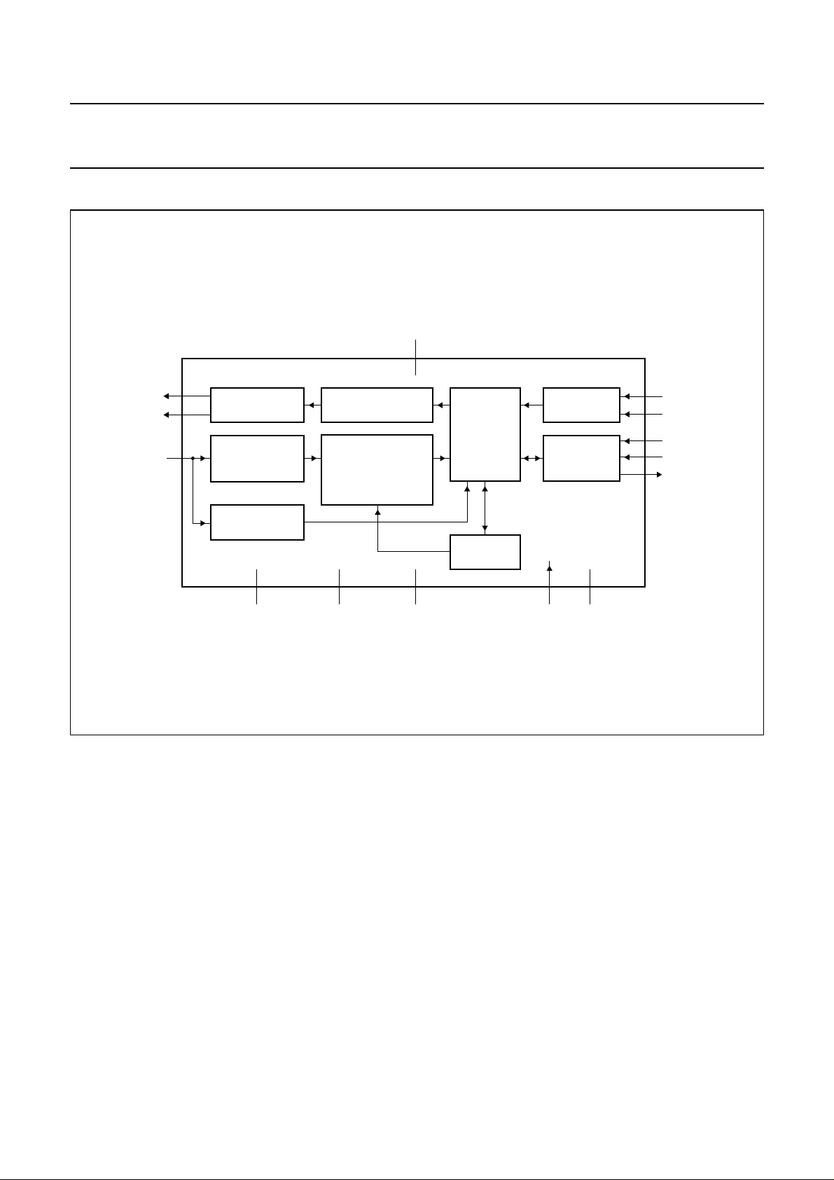
6 BLOCK DIAGRAM
handbook, full pagewidth
TX1
TX2
RX
4
2
14
SYNCHRONOUS
DEMODULATOR
MEASUREMENT
V
DD
3
ANTENNA
DRIVERS
PHASE
13 12 11
MODULATOR
BANDPASS FILTER
AMPLIFIER
DYNAMIC CONTROL
DIGITIZER
V
SS
CONTROL
UNIT
CONTROL
REGISTER
1
MODE
Fig.1 Block diagram.
OSCILLATOR
SERIAL
INTERFACE
HTRC11001T
5
n.c.CEXTQGND
10
MGW265
6
XTAL1
7
XTAL2
8
SCLK
9
DIN
DOUT
2001 Nov 23 4
Philips Semiconductors Product specification
HITAG reader chip HTRC11001T
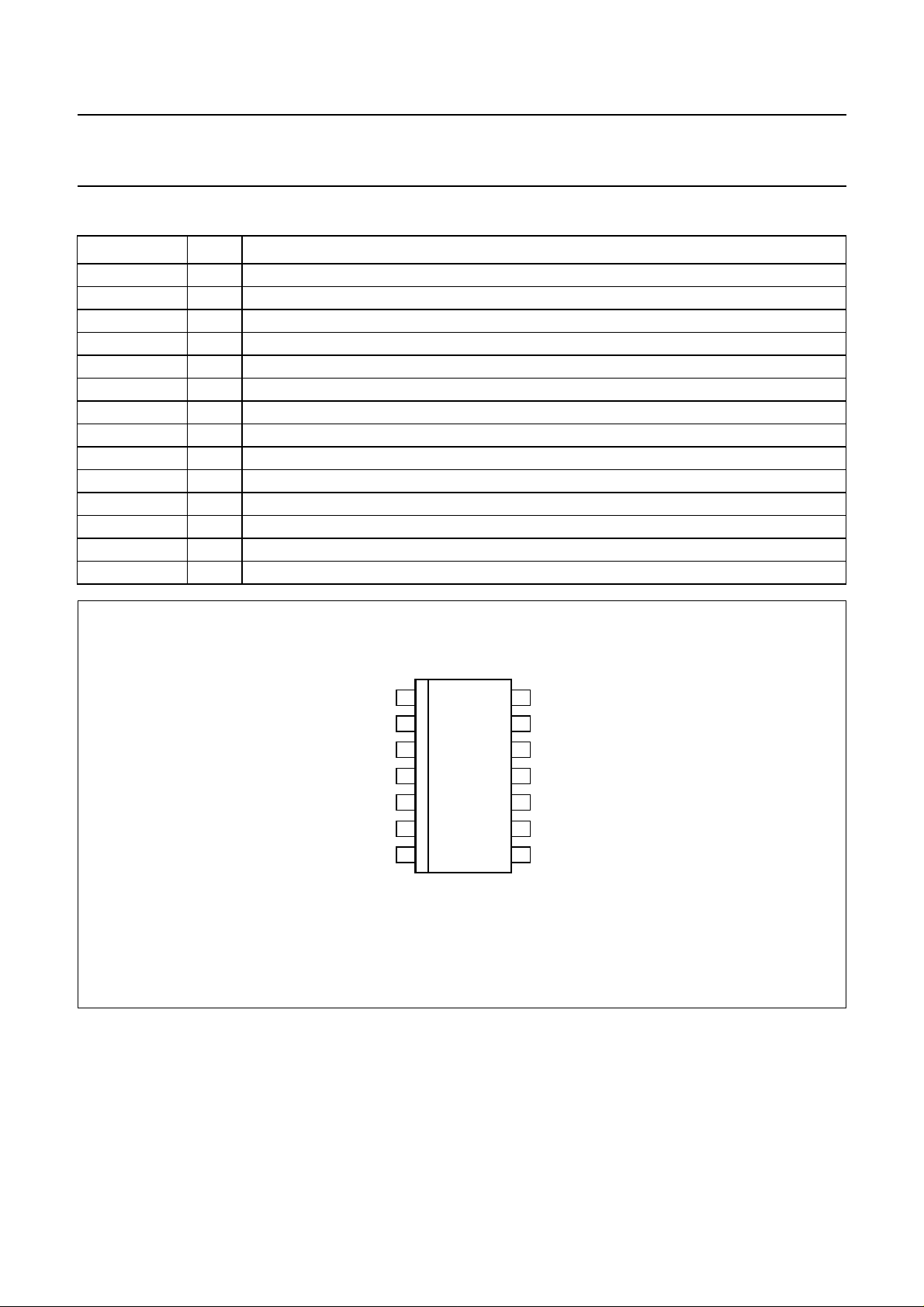
7 PINNING
SYMBOL PIN DESCRIPTION
V
SS
TX2 2 antenna driver output 2
V
DD
TX1 4 antenna driver output 1
MODE 5 control input to enable filtering of serial clock and data input; for active antenna applications
XTAL1 6 oscillator input 1
XTAL2 7 oscillator input 2
SCLK 8 serial clock input of microcontroller interface
DIN 9 serial data input of microcontroller interface
DOUT 10 serial data output of microcontroller interface
n.c. 11 not connected
CEXT 12 high-pass filter coupling capacitor connection
QGND 13 internal analog virtual ground capacitor connection
RX 14 demodulator input
1 ground supply
3 supply voltage (5 V stabilized)
handbook, halfpage
V
1
SS
TX2
2
3
V
DD
4
TX1
MODE
XTAL1
XTAL2
HTRC11001T
5
6
7
Fig.2 Pin configuration.Fig.2 Pin configuration.
MGW266
14
13
12
11
10
9
8
RX
QGND
CEXT
n.c.
DOUT
DIN
SCLK
2001 Nov 23 5

Philips Semiconductors Product specification
HITAG reader chip HTRC11001T
8 FUNCTIONAL DESCRIPTION
8.1 Power supply
TheHTRC11001Tworkswithan external 5 V ±10% power
supply at pin VDD. The maximum DC current is
10 mA + × I
2
-- -
π
ant(p)
= 137 mA.
For optimum performance, the power supply connection
should be bypassed to ground with a 100 nF capacitor
close to the chip.
8.2 Antenna drivers
The drivers deliver a square shaped voltage to the series
resonant antenna circuit (see Fig.4). Due to the full bridge
configuration of the drivers the output voltage V
approximately 10 V, corresponding to V
ant(p)
=5V.
ant(p-p)
is
The current flowing through the antenna is sine shaped
and the peak and RMS values are approximately:
V
4
I
ant(p)
I
ant(rms)
ant(p)
×=
--------------- -
-- -
π
R
ant
1
×=
I
-------
ant(p)
2
8.3 Diagnosis
In order to detect an antenna short-circuit or open-circuit
the antenna tap voltage is monitored.
An antenna fail condition is reported in the status
bit ANTFAIL (see Table 5) if the antenna tap voltage does
not go more negative than the diagnosis level voltage
(V
= −1.15 V). This condition is checked for every coil
diag
driver cycle.
8.5 Adaptive sampling time demodulator
The demodulator senses the absorption modulation
applied by a transponder when inserted into the field. The
signal is picked up at the antenna tap point between
L
and Ca. It is divided by Rv and the internal resistor R
a
int
to a level on pin RX below 8 V (peak value) with respect to
pin QGND (see Fig.4). Internally the signal is filtered with
a second-order low-pass filter.
The antenna current and therefore the tap voltage is
modulated by the transponder in amplitude and/or phase.
This signal is fed into a synchronous demodulator
recovering the baseband signal. The amplification and the
bandpass filter edge frequencies of the demodulator can
be adapted to different transponders via settings in the
configuration pages (see Table 3).
The phase between the driver excitation signal and the
antenna tap voltage depends on the antenna tuning. With
optimum tuning, the phase of the antenna tap voltage is
90° off the antenna driver signal. Detuning of the antenna
resonant circuit results in a change of this phase
relationship. The built-in phase measurement unit allows
the measurement of this phase relationship with a
resolution of . This can be used to
-----64
1
360°× 5.625°=
compute a sampling time that compensates the detuning
of the reader antenna.
The phase measurement procedure can be carried out:
• Once before the first communication starts, if the
position of the transponder does not change with
respect to the reader antenna
• During the communication (after sending the write
pulses and before receiving the answer of the
transponder), if the tag is moving.
8.4 Oscillator with programmable divider
Thecrystaloscillatoratpins XTAL1and XTAL2workswith
either crystal or ceramic resonators. It delivers the input
clock frequency of 4, 8, 12 or 16 MHz. The oscillator
frequency is divided by a programmable divider (selection
bits FSEL1 and FSEL0) to obtain the carrier frequency of
125 kHz (see Table 3).
Alternatively, an external clock signal (CMOS compatible)
may connected to pin XTAL1. For example, this clock
signal can be derived from the microcontroller clock.
2001 Nov 23 6
Beforethesystemisswitched into WRITE_TAG mode, the
demodulator has to be frozen. This is internally done by
clamping the input of the filter amplifier unit to the level on
pin QGND. Doing so avoids large transients in the
amplifier and digitizer, which could affect settling times.
In addition to the clamping, there exist other means in the
HTRC11001T which allow further reduction of the settling
times. All the parts of the circuitry which are associated
with these functions are controlled by the bits FREEZE0,
FREEZE1 and THRESET (see Table 2).
For more details concerning write timing, demodulator
setting, power-up sequence, etc. please refer to the
application note
the HITAG Read/Write IC HTRC110”
“AN 98080 Read/Write devices based on
.
 Loading...