

Philips FB2031BB, CD3206BB Datasheet

INTEGRATED CIRCUITS
FB2031
9-bit latched/registered/pass-thru
Futurebus+ transceiver
Product specification
IC19 Data Handbook
1995 May 25

Philips Semiconductors Product specification
FB20319-bit latched/registered/pass-thru Futurebus+ transceiver
FEA TURES
•Latched, registered or straight through in
either A to B or B to A path
•Drives heavily loaded backplanes with
equivalent load impedances down to 10Ω.
•High drive 100mA BTL open collector
drivers on B-port
•Allows incident wave switching in heavily
loaded backplane buses
•Reduced BTL voltage swing produces less
noise and reduces power consumption
•Built-in precision band-gap reference
provides accurate receiver thresholds and
improved noise immunity
•Compatible with IEEE Futurebus+ or
proprietary BTL backplanes
•Each BTL driver has a dedicated Bus GND
for a signal return
•Controlled output ramp and multiple GND
pins minimize ground bounce
•Glitch-free power up/power down operation
•Low I
current
CC
•Tight output skew
•Supports live insertion
QUICK REFERENCE DATA
SYMBOL PARAMETER TYPICAL UNIT
t
PLH
t
PHL
t
PLH
t
PHL
C
I
I
O
OL
CC
Propagation delay
An to Bn
Propagation delay
Bn to An
2.7 ns
4.4
4.2
Output capacitance (B0 – Bn only) 6 pF
Output current (B0 – Bn only) 100 mA
Supply current
AIn to Bn
(outputs Low or High)
Bn to AOn (outputs Low) 50 mA
17 mA
Bn to AOn (outputs High) 25
ORDERING INFORMATION
PACKAGE
COMMERCIAL RANGE
VCC = 5V±10%; T
= 0°C to +70°C
amb
VCC = 5V±10%; T
52-pin Plastic Quad Flat Pack (QFP) FB2031BB CD3206BB SOT379-1
INDUSTRIAL RANGE
= –40°C to +85°C
amb
DRAWING
NUMBER
ns
PIN CONFIGURATION
LOGIC GND
LOGIC GND
LOGIC GND
LOGIC GND
LOGIC GND
LOGIC GND
LOGIC GND
CC
V
LOGIC GND
A1
A0
52 51 50 49 48 47 46 45 44 43 42 41 40
1
2
A2
3
4
A3
A4
A5
A6
A7
9-Bit latched/registered transceiver
5
6
7
8
9
10
11
12
13
14 15 16 17 18 19 20 21 22 23 24 25 26
A8
SEL1
LCBA
OEA
BIAS V
OEB0
FB2031
52-lead PQFP
CC
BG V
LCAB
SEL0
BG GND
CC
TCK (option)
V
OEB1
CC
V
TDI (option)
TDO (option)
TMS (option)
B0
BUS GND
39
38
37
36
35
34
33
32
31
30
29
28
27
B8
B7
BUS GND
BUS GND
B1
BUS GND
B2
BUS GND
B3
BUS GND
B4
BUS GND
B5
BUS GND
B6
BUS GND
SG00060
1995 May 25 853-1714 15279
2

Philips Semiconductors Product specification
FB20319-bit latched/registered/pass-thru Futurebus+ transceiver
DESCRIPTION
The FB2031 is a 9-bit latched/registered
transceiver featuring a latched, registered or
pass-thru mode in either the A-to-B or B-to-A
direction. The FB2031 is intended to provide
the electrical interface to a high performance
wired-OR bus.
The TTL-level side (A port) has a common
I/O. The common I/O, open collector B port
operates at BTL signal levels. The logic
element for data flow in each direction is
controlled by two mode select inputs (SEL0
and SEL1). A “00” configures latches in both
directions. A “10” configures thru mode in
both directions. A “01” configures register
mode in both directions. A “11” configures
register mode in the A-to-B direction and
latch mode in the B-to-A direction.
When configured in the buffer mode, the
inverse of the input data appears at the
output port. In the register mode, data is
stored on the rising edge of the appropriate
clock input (LCAB or LCBA). In the latch
mode, clock pins serve as transparent-Low
latch enables. Regardless of the mode, data
is inverted from input to output.
The 3-State A port is enabled by asserting a
High level on OEA. The B port has two output
enables, OEB0 and OEB1
is High and OEB1
enabled.
. Only when OEB0
is Low is the output
When either OEB0 is Low or OEB1
the B port is inactive and is pulled to the level
of the pullup voltage. New data can be
entered in the register and latched modes or
can be retained while the associated outputs
are in 3-State (A port) or inactive (B port).
The B-port drivers are Low-capacitance open
collectors with controlled ramp and are
designed to sink 100mA. Precision band gap
references on the B-port insure very good
noise margins by limiting the switching
threshold to a narrow region centered at
1.55V.
The B-port interfaces to “Backplane
Transceiver Logic” (see the IEEE 1194.1 BTL
standard). BTL features low power
consumption by reducing voltage swing (1V
p-p, between 1V and 2V) and reduced
capacitive loading by placing an internal
series diode on the drivers. BTL also
provides incident wave switching, a necessity
for high performance backplanes.
Output clamps are provided on the BTL
outputs to further reduce switching noise.
The “V
effects during a Low-to-High transition. The
“V
clamp, the “trapped reflection” clamp, clamps
out ringing below the BTL 0.5V V
This clamp remains active for approximately
100ns after a High-to-Low transition.
” clamp reduces inductive ringing
OH
” clamp is always active. The other
OH
is High,
level.
OL
To support live insertion, OEB0 is held Low
during power on/off cycles to insure glitchfree B port drivers. Proper bias for B port
drivers during live insertion is provided by the
BIAS V pin when at a 5V level while V
Low. The BIAS V pin is a low current input
which will reverse-bias the BTL driver series
Schottky diode, and also bias the B port
output pins to a voltage between 1.62V and
2.1V. This bias function is in accordance with
IEEE BTL Standard 1194.1. If live insertion is
not a requirement, the BIAS V pin should be
tied to a V
The LOGIC GND and BUS GND pins are
isolated inside the package to minimize noise
coupling between the BTL and TTL sides.
These pins should be tied to a common
ground external to the package.
Each BTL driver has an associated BUS
GND pin that acts as a signal return path and
these BUS GND pins are internally isolated
from each other. In the event of a ground
return fault, a “hard” signal failure occurs
instead of a pattern dependent error that may
be infrequent and impossible to troubleshoot.
As with any high power device, thermal
considerations are critical. It is
recommended that airflow (300Ifpm)
and/or thermal mounting be used to
ensure proper junction temperature.
CC
pin.
CC
is
P ACKAGE THERMAL CHARACTERISTICS
PARAMETER CONDITION 52-PIN PLASTIC QFP
θja Still air 80°C/W
θja 300 Linear feet per minute air flow 58°C/W
θjc Thermally mounted on one side to heat sink 20°C/W
PIN DESCRIPTION
SYMBOL PIN NUMBER TYPE NAME AND FUNCTION
A0 – A8 50, 52, 2, 4, 6, 8, 10, 12, 14 I/O BiCMOS data inputs/3-State outputs (TTL)
B0 – B8
OEB0 46 Input Enables the B outputs when High
OEB1 45 Input Enables the B outputs when Low
OEA 47 Input Enables the A outputs when High
BUS GND
LOGIC GND 51, 1, 3, 5, 7, 9, 11, 13 GND Logic ground (0V)
V
CC
BIAS V 48 Power Live insertion pre-bias pin
BG V
CC
BG GND 19 GND Band Gap threshold voltage reference ground
SEL0 20 Input Mode select
SEL1 15 Input Mode select
LCAB 18 Input A to B clock/latch enable (transparent latch when Low)
LCBA 16 Input B to A clock/latch enable (transparent latch when Low)
TMS 42 Input Test Mode Select (optional, if not implemented then no connect)
TCK 44 Input Test Clock (optional, if not implemented then no connect)
TDI 22 Input Test Data In (optional, if not implemented then no connect)
TDO 21 Output Test Data Out (optional, if not implemented then shorted to TDI)
40, 38, 36, 34, 32,
30, 28, 26, 24
25, 27, 29, 31, 33,
35, 37, 39, 41
23, 43, 49 Power Positive supply voltage
17 Power Band Gap threshold voltage reference
I/O Data inputs/Open Collector outputs, High current drive (BTL)
GND Bus ground (0V)
1995 May 25
3
Philips Semiconductors Product specification
MODE
An to Bn thru mode
An to Bn transparent latch
An to Bn latch and read
An to Bn register
Bn to An thru mode
Bn to An transparent latch
Bn to An latch and read
Bn to An register
Disable Bn outputs
Latch mode (Bn to An)
FB20319-bit latched/registered/pass-thru Futurebus+ transceiver
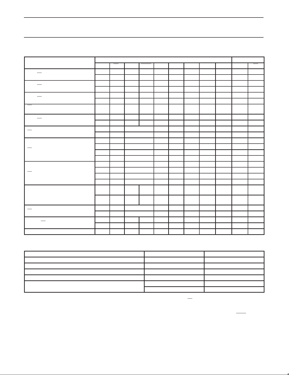
FUNCTION TABLE
INPUTS OUTPUTS
An Bn* OEB0 OEB1 OEA LCAB LCBA SEL0 SEL1 An Bn
L — H L L X X H L input H**
H — H L L X X H L input L
p
Bn outputs latched and read
(preconditioned latch)
p
An outputs latched and read
(preconditioned latch)
p
Disable An outputs X X X X L X X X X Z X
L — H L L L X L L input H**
H — H L L L X L L input L
l — H L L ↑ X L L input H**
h — H L L ↑ X L L input L
data
data
latched
data
X
X
X — H L X H X L L X
l — H L L ↑ X X H input H**
h — H L L ↑ X X H input L
— L Disable H X X H L H input
— H Disable H X X H L L input
— L Disable H X L L L H input
— H Disable H X L L L L input
— L Disable H X L H H H input
— H Disable H X L H H L input
— l Disable H X ↑ L L H input
— h Disable H X ↑ L L L input
— l Disable H X ↑ H H H input
— h Disable H X ↑ H H L input
— X X X H X H L L
— X X X H X H H H
— l Disable H X ↑ L H H input
— h Disable H X ↑ L H L input
X X L X X X X X X X H**
X X X H X X X X X X H**
latched
latched
FUNCTION SELECT TABLE
NOTES:
H = High voltage level
L = Low voltage level
l = Low voltage level one set-up time
prior to the Low-to-High LCXX transition
h = High voltage level one set-up time
prior to the Low-to-High LCXX transition
1995 May 25
MODE SELECTED SEL0 SEL1
Thru mode H L
Register mode (An to Bn) X H
Latch mode (An to Bn) L L
Register mode (Bn to An) L H
L L
H H
X = Don’t care
Z = High-impedance (OFF) state
— = Input not externally driven
↑ = Low-to-High transition
H** = Goes to level of pull-up voltage
4
Bn
* = Precaution should be taken to
ensure B inputs do not float. If they do, they
are equal to Low state.
Disable = OEB0 is Low or OEB1
is High.
Philips Semiconductors Product specification
FB20319-bit latched/registered/pass-thru Futurebus+ transceiver
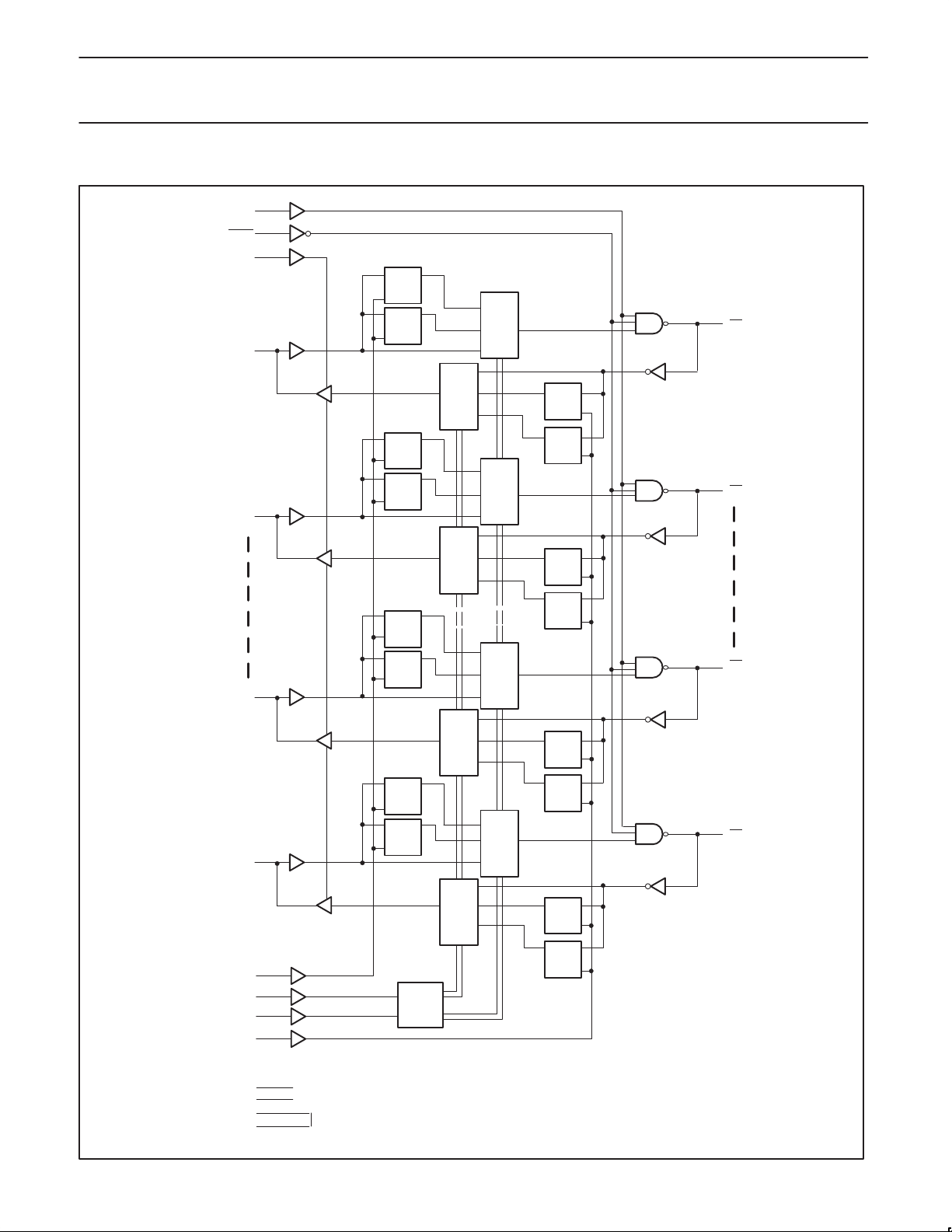
LOGIC DIAGRAM
46
OEB0
45
OEB1
47
OEA
DQ
E
DQ
14
A8
Clk
MUX
A ⇒ B
24
B8
TTL
MUX
A ⇐ B
DQ
E
DQ
12
A7
10
8
6
4
2
52
A1
50
A0
Clk
DQ
E
DQ
Clk
DQ
E
DQ
Clk
MUX
A ⇒ B
MUX
A ⇐ B
MUX
A ⇒ B
MUX
A ⇐ B
MUX
A ⇒ B
DQ
QD
E
DQ
Clk
DQ
E
DQ
Clk
DQ
E
DQ
Clk
26
B7
28
30
32
BTL
34
36
38
B1
40
B0
1995 May 25
LCAB
SEL0
SEL1
LCBA
TMS
TCK
TDI
TDO
18
20
15
16
42
(JTAG Boundary Scan pins)
44
22
21
Decode
OutIn
MUX
A ⇐ B
DQ
E
DQ
Clk
LOGIC GND = 1, 3, 5, 7, 9, 11, 13, 51
BUS GND = 25, 27, 29, 31, 33, 35, 37, 39, 41
BIAS V = 48
V
CC
BG V
BG GND = 19
CC
= 23, 43, 49
=17
SG00061
5
Philips Semiconductors Product specification
FB20319-bit latched/registered/pass-thru Futurebus+ transceiver
ABSOLUTE MAXIMUM RATINGS
Operation beyond the limits set forth in this table may impair the useful life of the device.
Unless otherwise noted these limits are over the operating free-air temperature range.
SYMBOL
V
T
V
V
I
OUT
I
OUT
STG
CC
IN
IN
Supply voltage -0.5 to +7.0 V
Input voltage All inputs except B0 – B8 -1.2 to +7.0 V
Input current -40 to +5.0 mA
Voltage applied to output in High output state -0.5 to +V
Current applied to output in Low output state A0 – A8 48 mA
Storage temperature -65 to +150 °C
RECOMMENDED OPERATING CONDITIONS (Industrial)
SYMBOL PARAMETER LIMITS UNIT
V
C
T
V
V
I
I
OH
I
I
amb
CC
IH
IL
IK
OL
IA
OB
Supply voltage 4.5 5.0 5.5 V
High-level input voltage Except B0–B8 2.0 V
Low-level input voltage Except B0 – B8 0.8 V
Input clamp current Control inputs -40 mA
High-level output current A0 – A8 -3 mA
Low-level output current A0 – A8 24 mA
Off device input current Except B0 – B8,
Output capacitance of B port 6 7 pF
Operating free-air temperature range –40 +85 °C
PARAMETER RATING UNIT
B0 – B8 -1.2 to +3.5
CC
V
B0 – B8 200
MIN TYP MAX
B0 – B8 1.62 1.55
B0 – B8 1.47
B0 – B8 & A0 – A8 -18
B0 – B8 100
100 µA
VI = 0 to 5.5V, VCC = 0V
RECOMMENDED OPERATING CONDITIONS (Commercial)
SYMBOL PARAMETER LIMITS UNIT
MIN TYP MAX
V
CC
V
IH
V
IL
I
IK
I
OH
I
OL
I
IA
C
OB
T
amb
1995 May 25
Supply voltage 4.5 5.0 5.5 V
High-level input voltage Except B0–B8 2.0 V
B0 – B8 1.62 1.55
Low-level input voltage Except B0 – B8 0.8 V
B0 – B8 1.47
Input clamp current Control inputs -40 mA
B0 – B8 & A0 – A8 -18
High-level output current A0 – A8 -3 mA
Low-level output current A0 – A8 24 mA
B0 – B8 100
Off device input current Except B0 – B8,
100 µA
VI = 0 to 5.5V, VCC = 0V
Output capacitance of B port 6 7 pF
Operating free-air temperature range 0 +70 °C
6
 Loading...