

Philips EJ3.0ULA Service Manual
Color Television Chassis
EJ3.0U
LA
G_16480_000.eps
060207
Contents Page Contents Page
1. Technical Specifications, Connections, and Chassis
Overview 2
2. Safety Instructions, Warnings, and Notes 6
3. Directions for Use 8
4. Mechanical Instructions 9
5. Service Modes, Error Codes, and Fault Finding 17
6. Block Diagrams, Test Point Overviews, and
Waveforms
Wiring Diagram 32” 37
Wiring Diagram 32” AL 38
Wiring Diagram 37”-42” 39
Block Diagram Video 40
Block Diagram Audio 41
Block Diagram Control & Clock Signals 42
Test Point Overview SSB 43-48
Test Point Overview AL Inter Conn. Panel 49
I2C IC’s Overview 50
Supply Lines Overview 51
7. Circuit Diagrams and PWB Layouts Diagram PWB
SSB: DC/DC (B01A) 52 84-89
SSB: Supply & RS232 (B01B) 53 84-89
SSB: Channel Decoder (B02A) 54 84-89
SSB: Main Tuner (B02B) 55 84-89
SSB: MPIF Main: Video Source Selection(B03A)56 84-89
SSB: MPIF Main: Supply (B03B) 57 84-89
SSB: MPIF Main: IF & SAW Filter (B03C) 58 84-89
SSB: MPIF Main: Audio Source Selection(B03D)59 84-89
SSB: MPIF Main: Audio Amplifier (B03E) 60 84-89
SSB: PNX2015: Audio / Video (B04A) 61 84-89
SSB: PNX2015: DV I/O Interface (B04B) 62 84-89
SSB: PNX2015: Tunnelbus (B04C) 63 84-89
SSB: PNX2015: DDR Interface (B04D) 64 84-89
SSB: PNX2015: Standby & Control (B04E) 65 84-89
SSB: PNX2015: Supply (B04F) 66 84-89
©
Copyright 2007 Philips Consumer Electronics B.V. Eindhoven, The Netherlands.
All rights reserved. No part of this publication may be reproduced, stored in a
retrieval system or transmitted, in any form or by any means, electronic,
mechanical, photocopying, or otherwise without the prior permission of Philips.
SSB: VIPER/PNX2015: Display Interface(B04G)67 84-89
SSB: VIPER: Control (B05A) 68 84-89
SSB: VIPER: Main Memory (B05B) 69 84-89
SSB: VIPER: A/V & Tunnelbus (B05C) 70 84-89
SSB: VIPER: Supply (B05D) 71 84-89
SSB: VIPER: EEPROM (B05E) 72 84-89
SSB: VIPER: Miscellaneous (B05F) 73 84-89
SSB: Display Interface: MOP (B06) 74 84-89
SSB: HDMI & Supply (B07A) 75 84-89
SSB: HDMI I/O & Control (B07B) 76 84-89
SSB: Analog I/O (B07C) 77 84-89
SSB: Uart (B07D) 78 84-89
SSB: HDMI (B07E) 79 84-89
SSB: Audio: Amplifier (B08A) 80 84-89
SSB: Audio: Connectors (B08B) 81 84-89
SSB: SRP List 81-83
Side A/V Panel (D) 90 91
Keyboard Control Panel (E) 92 93
Front IR / LED Panel (J) 94
AL Inter Connect Panel: DC/DC Converter (M1) 96 101-102
AL Inter Connect Panel: Pacific 3 (M2) 97 101-102
AL Inter Connect Panel: Display Interface (M3) 98 101-102
AL Inter Connect Panel: Inter Connection (M4) 99 101-102
AL Inter Connect Panel: DC/DC Ambi (M5) 100 101-102
8. Alignments 103
9. Circuit Descriptions, Abbreviation List, and IC Data
Sheets 109
Abbreviation List 112
IC Data Sheets 114
10. Spare Parts List 125
11. Revision List 133
95
Published by WS 0762 BG CD Customer Service Printed in the Netherlands Subject to modification EN 3122 785 16840

EN 2 EJ3.0U LA1.
Technical Specifications, Connections, and Chassis Overview
1. Technical Specifications, Connections, and Chassis Overview
Index of this chapter:
1.1 Technical Specifications
1.2 Connection Overview
1.3 Chassis Overview
Notes:
• Some models in this chassis range have a different
mechanical construction. The information given here is
therefore model specific.
• Figures below can deviate slightly from the actual situation,
due to the different set executions.
• Specifications are indicative (subject to change).
1.1 Technical Specifications
1.1.1 Vision
Display type : LCD
Aspect ratio : 16: 9
Screen size(s) : 26” (67 cm)
: 32” (82 cm)
: 37” (94 cm)
: 42” (107 cm)
: 47” (119 cm)
Resolution :
- for 42 and 47PFL5422D/37 : 1920(*3) x 1080p
- for all other models : 1366(*3) x 768p
Typical contrast ratio : 700: 1 (26”)
Minimum light output (cd/m
Maximum response time (ms) : 15 (26”)
Viewing angle (HxV degrees) : 178 x 178
Tuning system : PLL
TV Color systems : ATSC, NTSC
Video playback : NTSC
Cable : Unscrambled digital
Tuner bands : VHF, UHF, S-
Supported video formats : 480i @ 60Hz
2
) : 500
: 800: 1 (32”)
: 1,000: 1 (37”)
: 1,000: 1 (42”)
: 800: 1 (47”)
: 9 (32”)
: 6 (37”)
: 5 (42”)
: 8 (47”)
cable - QAM
channel, Hyperband
: 480p @ 60Hz
: 720p @ 60Hz
: 1080i @ 60Hz
1.1.4 Miscellaneous
Power supply:
- Mains voltage (V
Ambient conditions:
- Temperature range (°C) : +5 to +35
- Maximum humidity : 90% R.H.
Power consumption:
- Normal operation (W) : 125 (26”)
- Stand-by (W) : < 1
Dimensions (W x H x D in inches) : TBF (26”)
Weight, stand included (kg/lbs) : TBF (26”)
) : 110 - 240
AC
: 155 (32”)
: 210 (37”)
: 275 (42”)
:TBF (47”)
: 31.7 x 24.0 x 8.3 (32”)
: 36.7 x 24.6 x 4.7 (37”)
: 41.1 x 27.0 x 4.5 (42”)
:TBF (47”)
: 18 / 39.8 (32”)
: 26 / 57 (37”)
: 32 / 70.4 (42”)
:TBF (47”)
1.1.2 Sound
Sound systems : AV Stereo
Maximum power (W
1.1.3 Multimedia
Supported file formats : JPEG
USB input : USB1.1
) : 2 x 10 (26 and 32”)
RMS
:BTSC
: Dolby Digital (AC3)
: 2 x 15 (37, 42, 47 and
50”)
:MP3
: Slideshow (.alb)
Technical Specifications, Connections, and Chassis Overview
1.2 Connection Overview
Note: The following connector color abbreviations are used
(acc. to DIN/IEC 757): Bk= Black, Bu= Blue, Gn= Green, Gy=
Grey, Rd= Red, Wh= White, and Ye= Yellow.
REAR CONNECTIONS
EN 3EJ3.0U LA 1.
SIDE A/V
Figure 1-1 Rear and side A/V connections
1.2.1 Side Connections
USB1.1
1234
E_06532_022.eps
300904
Figure 1-2 USB (type A)
1-+5V k
2 -Data (-) jk
3 -Data (+) jk
4 -Ground Gnd H
Mini Jack: Audio Headphone - Out
Bk - Headphone 32 - 600 ohm / 10 mW ot
Cinch: Video CVBS - In, Audio - In
Ye - Video CVBS 1 V
Wh - Audio L 0.5 V
Rd - Audio R 0.5 V
/ 75 ohm jq
PP
/ 10 kohm jq
RMS
/ 10 kohm jq
RMS
S-Video (Hosiden): Video Y/C - In
1 -Ground Y Gnd H
2 -Ground C Gnd H
3 - Video Y 1 V
4 - Video C 0.3 V
/ 75 ohm j
PP
P / 75 ohm j
PP
1.2.2 Rear Connections
AV2 Cinch: Video YPbPr - In
Gn - Video Y 1 V
Bu - Video Pb 0.7 V
Rd - Video Pr 0.7 V
/ 75 ohm jq
PP
/ 75 ohm jq
PP
/ 75 ohm jq
PP
AV2 Cinch: Audio - In
Wh - Audio L 0.5 V
Rd - Audio R 0.5 V
/ 10 kohm jq
RMS
/ 10 kohm jq
RMS
Cinch: S/PDIF - Out
Bk - Coaxial 0.4 - 0.6V
/ 75 ohm kq
PP
G_16840_093.eps
060207
AV1 Cinch: Video YPbPr - In
Gn - Video Y 1 V
Bu - Video Pb 0.7 V
Rd - Video Pr 0.7 V
/ 75 ohm jq
PP
/ 75 ohm jq
PP
/ 75 ohm jq
PP
AV1 Cinch: Video CVBS - In
Ye - Video CVBS 1 V
/ 75 ohm jq
PP
AV1 Cinch: Audio - In
Wh - Audio L 0.5 V
Rd - Audio R 0.5 V
/ 10 kohm jq
RMS
/ 10 kohm jq
RMS
HDMI 1 & HDMI 2: Digital Video, Digital Audio - In
19
18 2
1
E_06532_017.eps
250505
Figure 1-3 HDMI (type A) connector
1 - D2+ Data channel j
2 - Shield Gnd H
3 - D2- Data channel j
4 - D1+ Data channel j
5 - Shield Gnd H
6 - D1- Data channel j
7 - D0+ Data channel j
8 - Shield Gnd H
9 - D0- Data channel j
10 - CLK+ Data channel j
11 - Shield Gnd H
12 - CLK- Data channel j
13 - n.c.
14 - n.c.
15 - DDC_SCL DDC clock j
16 - DDC_SDA DDC data jk
17 - Ground Gnd H
18 - +5V j
19 - HPD Hot Plug Detect j
20 - Ground Gnd H
Aerial - In
- - F-type (US) Coax, 75 ohm D

EN 4 EJ3.0U LA1.
1.3 Chassis Overview
POWER SUPPLY
A
Technical Specifications, Connections, and Chassis Overview
AMBILIGHT INTER-
CONNECTION
BOARD
SIDE I/O
BOARD
M
D
SMALL SIGNAL
B
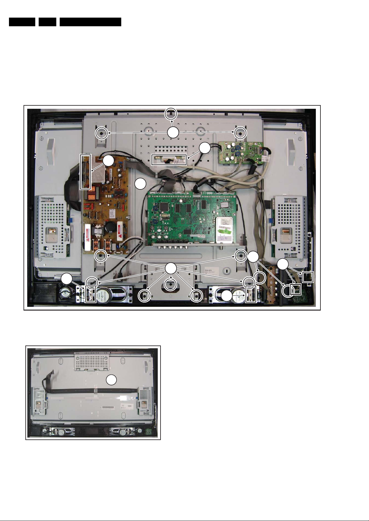
BOARD
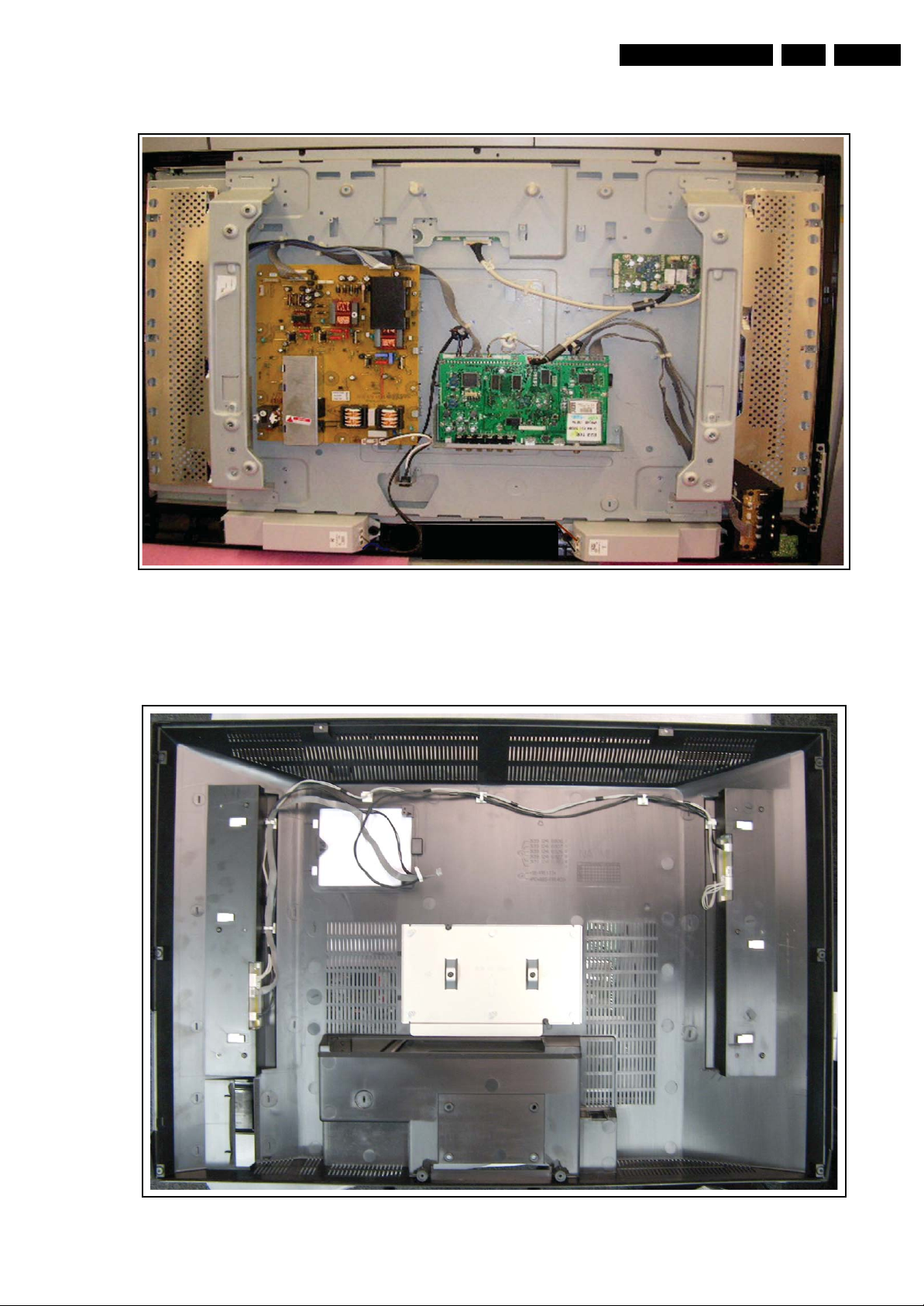
Figure 1-4 PWB/CBA locations (26-inch model)
G_16840_094.eps
070207
CONTROL
BOARD
IR / LED
BOARD
AMBILIGHT INTER-
CONNECTION
BOARD
E
J
M
POWER SUPPLY
A
SMALL SIGNAL
B
BOARD
Figure 1-5 PWB/CBA locations (32-inch model)
G_16840_013.eps
060207
SIDE I/O
BOARD
CONTROL
BOARD
IR / LED
BOARD
D
E
J
Technical Specifications, Connections, and Chassis Overview
EN 5EJ3.0U LA 1.
AMBILIGHT INTER-
CONNECTION
BOARD
M
POWER SUPPLY
A
SMALL SIGNAL
B
BOARD
Figure 1-6 PWB/CBA locations (37-inch model)
G_16840_095.eps
080207
SIDE I/O
BOARD
CONTROL
BOARD
IR / LED
BOARD
D
E
J
POWER SUPPLY
A
SMALL SIGNAL
B
BOARD
Figure 1-7 PWB/CBA locations (42-inch model)
G_16840_096.eps
070207
AMBILIGHT INTER-
CONNECTION
BOARD
SIDE I/O
BOARD
CONTROL
BOARD
IR / LED
BOARD
M
D
E
J

EN 6 EJ3.0U LA2.
Safety Instructions, Warnings, and Notes
2. Safety Instructions, Warnings, and Notes
Index of this chapter:
2.1 Safety Instructions
2.2 Warnings
2.3 Notes
2.1 Safety Instructions
Safety regulations require the following during a repair:
• Connect the set to the Mains/AC Power via an isolation
transformer (> 800 VA).
• Replace safety components, indicated by the symbol h,
only by components identical to the original ones. Any
other component substitution (other than original type) may
increase risk of fire or electrical shock hazard.
Safety regulations require that after a repair, the set must be
returned in its original condition. Pay in particular attention to
the following points:
• Route the wire trees correctly and fix them with the
mounted cable clamps.
• Check the insulation of the Mains/AC Power lead for
external damage.
• Check the strain relief of the Mains/AC Power cord for
proper function.
• Check the electrical DC resistance between the Mains/AC
Power plug and the secondary side (only for sets that have
a Mains/AC Power isolated power supply):
1. Unplug the Mains/AC Power cord and connect a wire
between the two pins of the Mains/AC Power plug.
2. Set the Mains/AC Power switch to the "on" position
(keep the Mains/AC Power cord unplugged!).
3. Measure the resistance value between the pins of the
Mains/AC Power plug and the metal shielding of the
tuner or the aerial connection on the set. The reading
should be between 4.5 Mohm and 12 Mohm.
4. Switch "off" the set, and remove the wire between the
two pins of the Mains/AC Power plug.
• Check the cabinet for defects, to prevent touching of any
inner parts by the customer.
2.2 Warnings
• All ICs and many other semiconductors are susceptible to
electrostatic discharges (ESD w). Careless handling
during repair can reduce life drastically. Make sure that,
during repair, you are connected with the same potential as
the mass of the set by a wristband with resistance. Keep
components and tools also at this same potential. Available
ESD protection equipment:
– Complete kit ESD3 (small tablemat, wristband,
connection box, extension cable and earth cable) 4822
310 10671.
– Wristband tester 4822 344 13999.
• Be careful during measurements in the high voltage
section.
• Never replace modules or other components while the unit
is switched "on".
• When you align the set, use plastic rather than metal tools.
This will prevent any short circuits and the danger of a
circuit becoming unstable.
2.3 Notes
2.3.1 General
• Measure the voltages and waveforms with regard to the
chassis (= tuner) ground (H), or hot ground (I), depending
on the tested area of circuitry. The voltages and waveforms
shown in the diagrams are indicative. Measure them in the
Service Default Mode (see chapter 5) with a color bar
signal and stereo sound (L: 3 kHz, R: 1 kHz unless stated
otherwise) and picture carrier at 475.25 MHz for PAL, or
61.25 MHz for NTSC (channel 3).
• Where necessary, measure the waveforms and voltages
with (D) and without (E) aerial signal. Measure the
voltages in the power supply section both in normal
operation (G) and in stand-by (F). These values are
indicated by means of the appropriate symbols.
2.3.2 Schematic Notes
• All resistor values are in ohms, and the value multiplier is
often used to indicate the decimal point location (e.g. 2K2
indicates 2.2 kohm).
• Resistor values with no multiplier may be indicated with
either an "E" or an "R" (e.g. 220E or 220R indicates 220
ohm).
• All capacitor values are given in micro-farads (μ= x10
nano-farads (n= x10
• Capacitor values may also use the value multiplier as the
decimal point indication (e.g. 2p2 indicates 2.2 pF).
• An "asterisk" (*) indicates component usage varies. Refer
to the diversity tables for the correct values.
• The correct component values are listed in the Spare Parts
List. Therefore, always check this list when there is any
doubt.
2.3.3 BGA (Ball Grid Array) ICs
Introduction
For more information on how to handle BGA devices, visit this
URL: www.atyourservice.ce.philips.com (needs subscription,
not available for all regions). After login, select “Magazine”,
then go to “Repair downloads”. Here you will find Information
on how to deal with BGA-ICs.
BGA Temperature Profiles
For BGA-ICs, you must use the correct temperature-profile,
which is coupled to the 12NC. For an overview of these profiles,
visit the website www.atyourservice.ce.philips.com (needs
subscription, but is not available for all regions)
You will find this and more technical information within the
"Magazine", chapter "Repair downloads".
For additional questions please contact your local repair help
desk.
2.3.4 Lead-free Soldering
Due to lead-free technology some rules have to be respected
by the workshop during a repair:
• Use only lead-free soldering tin Philips SAC305 with order
code 0622 149 00106. If lead-free solder paste is required,
please contact the manufacturer of your soldering
equipment. In general, use of solder paste within
workshops should be avoided because paste is not easy to
store and to handle.
• Use only adequate solder tools applicable for lead-free
soldering tin. The solder tool must be able:
– To reach a solder-tip temperature of at least 400°C.
– To stabilize the adjusted temperature at the solder-tip.
– To exchange solder-tips for different applications.
• Adjust your solder tool so that a temperature of around
360°C - 380°C is reached and stabilized at the solder joint.
Heating time of the solder-joint should not exceed ~ 4 sec.
Avoid temperatures above 400°C, otherwise wear-out of
tips will increase drastically and flux-fluid will be destroyed.
To avoid wear-out of tips, switch “off” unused equipment or
reduce heat.
-9
), or pico-farads (p= x10
-12
-6
),
).

Safety Instructions, Warnings, and Notes
• Mix of lead-free soldering tin/parts with leaded soldering
tin/parts is possible but PHILIPS recommends strongly to
avoid mixed regimes. If this cannot be avoided, carefully
clear the solder-joint from old tin and re-solder with new tin.
2.3.5 Alternative BOM identification
The third digit in the serial number (example:
AG2B0335000001) indicates the number of the alternative
B.O.M. (Bill Of Materials) that has been used for producing the
specific TV set. In general, it is possible that the same TV
model on the market is produced with e.g. two different types
of displays, coming from two different suppliers. This will then
result in sets which have the same CTN (Commercial Type
Number; e.g. 28PW9515/12) but which have a different B.O.M.
number.
By looking at the third digit of the serial number, one can
identify which B.O.M. is used for the TV set he is working with.
If the third digit of the serial number contains the number “1”
(example: AG1B033500001), then the TV set has been
manufactured according to B.O.M. number 1. If the third digit is
a “2” (example: AG2B0335000001), then the set has been
produced according to B.O.M. no. 2. This is important for
ordering the correct spare parts!
For the third digit, the numbers 1...9 and the characters A...Z
can be used, so in total: 9 plus 26= 35 different B.O.M.s can be
indicated by the third digit of the serial number.
EN 7EJ3.0U LA 2.
Identification: The bottom line of a type plate gives a 14-digit
serial number. Digits 1 and 2 refer to the production center (e.g.
AG is Bruges), digit 3 refers to the B.O.M. code, digit 4 refers
to the Service version change code, digits 5 and 6 refer to the
production year, and digits 7 and 8 refer to production week (in
example below it is 2006 week 17). The 6 last digits contain the
serial number.
MODEL :
PROD.NO:
32PF9968/10
AG 1A0617 000001
MADE IN BELGIUM
220-240V 50/60Hz
~
VHF+S+H+UHF
BJ3.0E LA
S
E_06532_024.eps
Figure 2-1 Serial number (example)
2.3.6 Board Level Repair (BLR) or Component Level Repair
(CLR)
If a board is defective, consult your repair procedure to decide
if the board has to be exchanged or if it should be repaired on
component level.
If your repair procedure says the board should be exchanged
completely, do not solder on the defective board. Otherwise, it
cannot be returned to the O.E.M. supplier for back charging!
128W
130606
2.3.7 Practical Service Precautions
• It makes sense to avoid exposure to electrical shock.
While some sources are expected to have a possible
dangerous impact, others of quite high potential are of
limited current and are sometimes held in less regard.
• Always respect voltages. While some may not be
dangerous in themselves, they can cause unexpected
reactions that are best avoided. Before reaching into a
powered TV set, it is best to test the high voltage insulation.
It is easy to do, and is a good service precaution.

EN 8 EJ3.0U LA3.
3. Directions for Use
You can download this information from the following websites:
http://www.philips.com/support
http://www.p4c.philips.com
Directions for Use

4. Mechanical Instructions
Mechanical Instructions
EN 9EJ3.0U LA 4.
Index of this chapter:
4.1 Cable Dressing
4.2 Service Positions
4.3 Assy/Panel Removal
4.4 Set Re-assembly
Notes:
• Several models in this chassis range have a different
mechanical construction, the instructions given in this
chapter are therefore very model specific.
4.1 Cable Dressing
• Figures below are taken from the 32PFL7332D/37 model,
and can deviate from the actual situation, due to the
different set executions.
• The EJ3.0U LA chassis is based on the EL1.1U chassis. If
the situation at hand differs too much from the description
below, please refer to the manual of that chassis (12NC:
312278516290).
• Follow the disassembly instructions in described order.
Figure 4-1 Cable dressing (26-inch model)
G_16840_090.eps
070207
EN 10 EJ3.0U LA4.
Mechanical Instructions
Figure 4-2 Cable dressing (32-inch model)
G_16840_080.eps
010207
Figure 4-3 Cable dressing (37-inch model)
G_16840_091.eps
060207
Mechanical Instructions
EN 11EJ3.0U LA 4.
Figure 4-4 Cable dressing (42-inch model)
G_16840_092.eps
060207
Figure 4-5 Cable dressing rear cover for models with AmbiLight (32-inch model)
G_16840_081.eps
010207
EN 12 EJ3.0U LA4.
Mechanical Instructions
4.2 Service Positions
For easy servicing of this set, there are a few possibilities
created:
• The buffers from the packaging.
• Foam bars (created for Service).
• Aluminium service stands (created for Service).
4.2.1 Foam Bars
1
Required for sets
1
42”
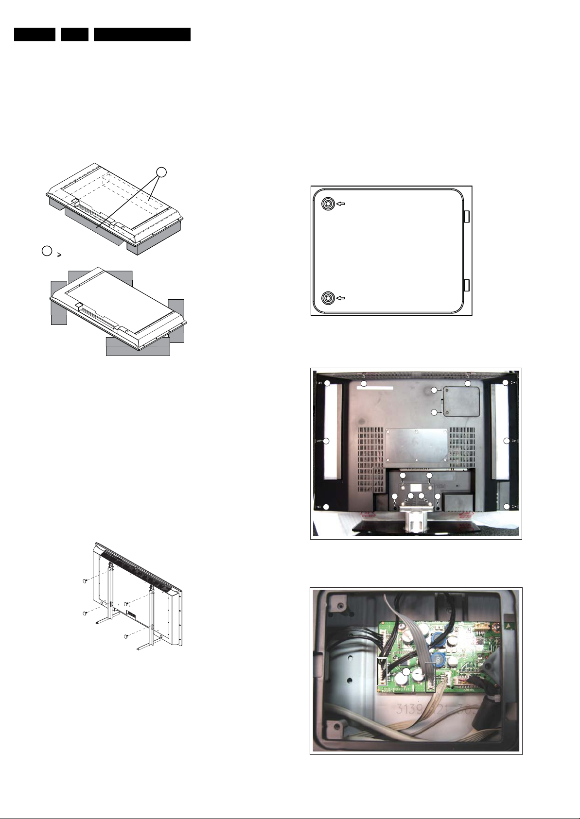
4.3 Assy/Panel Removal
4.3.1 Rear Cover
Warning: Disconnect the mains power cord before you remove
the rear cover.
1. Place the TV set upside down on a table top, using the
foam bars (see part "Service Position").
2. Remove screws [1] and the stand.
3. Remove screws [2] and the small “Service door”.
4. Unplug connectors [3]. See figure “Rear cover removal 2”
5. Remove screws [4] and the rear cover.
Open this Door to Disconnect connector
SERVICE WARNING!
before removing back-cover
G_16840_089.eps
060207
E_06532_018.eps
171106
Figure 4-6 Foam bars
The foam bars (order code 3122 785 90580 for two pieces) can
be used for all types and sizes of Flat TVs. See figure “Foam
bars” for details. Sets with a display of 42” and larger, require
four foam bars [1]. Ensure that the foam bars are always
supporting the cabinet and never only the display. Caution:
Failure to follow these guidelines can seriously damage the
display!
By laying the TV face down on the (ESD protective) foam bars,
a stable situation is created to perform measurements and
alignments. By placing a mirror under the TV, you can monitor
the screen.
4.2.2 Aluminium Stands
Figure 4-8 Service door (example)
4
4
1 1
1
1
4
Figure 4-9 Rear cover removal [1/2]
2
2
44
44
4
4
4
G_16850_005.eps
110107
E_06532_019.eps
170504
Figure 4-7 Aluminium stands (drawing of MkI)
The new MkII aluminium stands (not on drawing) with order
code 3122 785 90690, can also be used to do measurements,
alignments, and duration tests. The stands can be
(dis)mounted quick and easy by means of sliding them in/out
the "mushrooms" (not valid for all models!). The new stands are
backwards compatible with the earlier models.
Important: For (older) FTV sets without these "mushrooms", it
is obligatory to use the provided screws, otherwise it is possible
to damage the monitor inside!
3
Figure 4-10 Rear cover removal [2/2]
G_16850_006.eps
110107

Mechanical Instructions
s
7
EN 13EJ3.0U LA 4.
4.3.2 AmbiLight Module
1. Remove the rear cover, as described earlier.
2. Unplug connectors [1].
3. Remove screws [2].
4. Slide the module to the left or the right, depending on the
position of the module, and remove it from the rear cover.
2
1
4.3.4 Side I/O Panel
1. Remove the rear cover, as described earlier.
2. Unplug connector [a].
3. Remove screws [b] and remove the complete module. One
of the screws is T10 tapping, the other one is T10 Parker.
See fig. “Side I/O module”.
4. Remove T10 Parker screw [c]. See fig. “Side I/O panel 1”.
5. Push catch [d] (located at the underside of the bracket) and
slide the unit to the right from its bracket [e]. See fig. “Side
I/O panel 2”.
6. To remove the PWB from its bracket, you have to lift the
catch [f] located on top of the headphone connector. At the
same time, slide the PWB out of its bracket [g]. See fig.
“Side I/O panel 3”.
When defective, replace the whole unit.
b (1x)
a
b (1x)
Figure 4-11 AmbiLight unit
4.3.3 Keyboard Control Panel
1. Remove the rear cover, as described earlier.
2. Refer to fig. “Keyboard control panel“ below.
3. Remove the T10 Parker screws [1].
4. Unplug connector [2].
5. Remove the unit.
6. Release clips [3] and remove the board.
When defective, replace the whole unit.
3
1
G_16840_088.eps
050207
Figure 4-13 Side I/O module
c
G_16860_066.ep
G_16860_075.eps
010207
01020
2
1
Figure 4-12 Keyboard control panel
G_16850_007.eps
090207
Figure 4-14 Side I/O panel [1/3] top side
EN 14 EJ3.0U LA4.
2e
Mechanical Instructions
4.3.6 Mid-range Speakers
1. Remove the rear cover, as described earlier.
2. Refer to fig. “Mid-range speakers“ below.
3. Unplug connectors [1].
4. Remove T10 Parker screws [2].
2d
2 1 2
G_16850_010.eps
110107
G_16860_076.eps
010207
Figure 4-18 Mid-range speakers
Figure 4-15 Side I/O panel [2/3] bottom side
g
2
f
Figure 4-16 Side I/O panel [3/3]
4.3.5 IR/LED Panel
1. Remove the rear cover, as described earlier.
2. Refer to fig. “IR/LED panel“ below.
3. Unplug connector(s) [1].
4. Release clip [2] and remove the board.
When defective, replace the whole unit.
G_16860_077.eps
010207
4.3.7 Tweeters
1. Remove the rear cover, as described earlier.
2. Refer to fig. “Tweeters” below.
3. Unplug connectors [1].
4. Remove T10 Parker screws [2].
2 1
Figure 4-19 Tweeters
4.3.8 Power Supply Board
1. Remove the rear cover, as described earlier.
2. Unplug connectors [1].
3. Remove the fixation screws [2].
4. Take the board out of its brackets (it hinges on the right
side).
G_16850_011.eps
2
110107
1
2
Figure 4-17 IR/LED panel
G_16850_009.eps
110107
1
2
2
G_16840_082.eps
Figure 4-20 Power supply board
310107
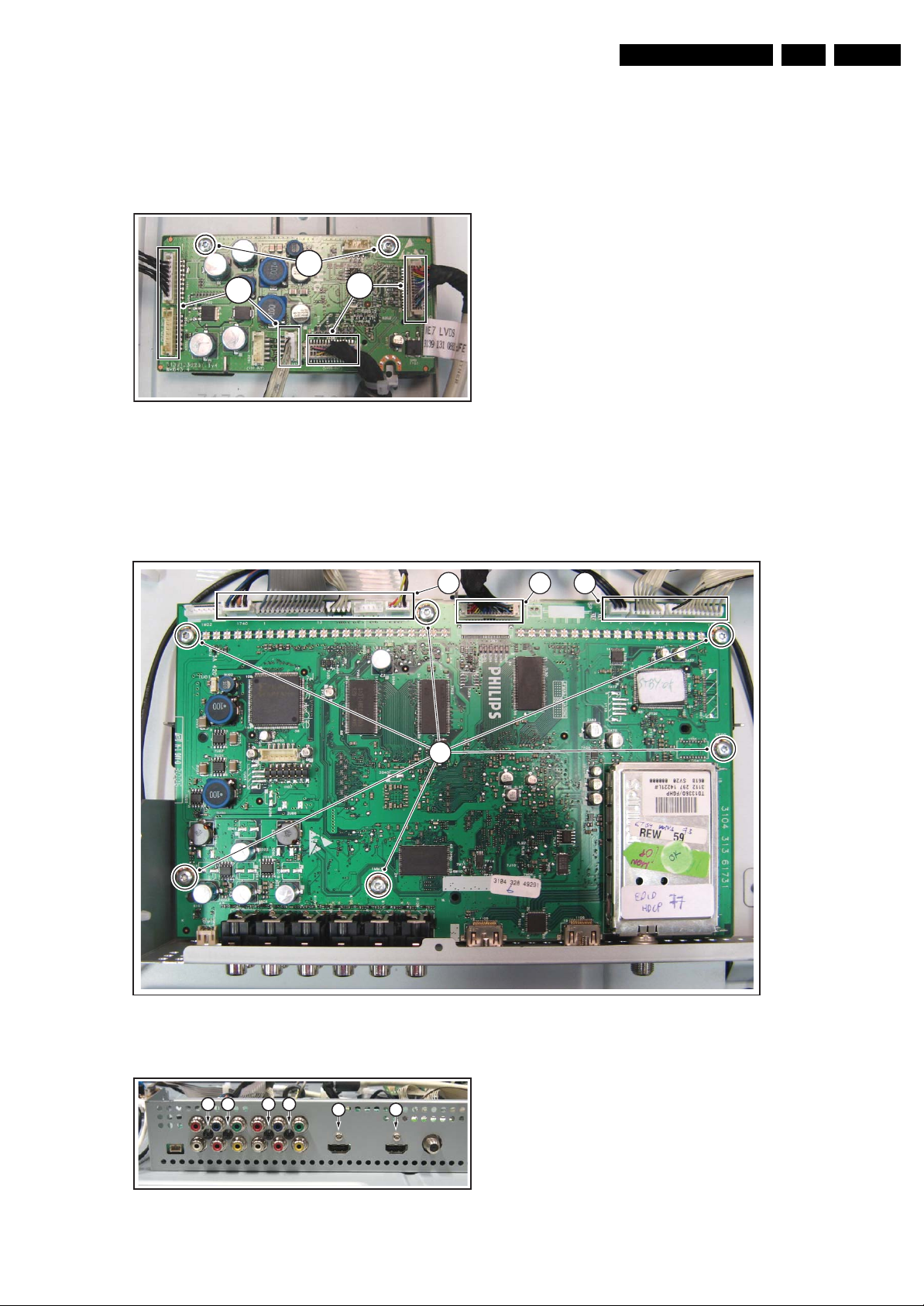
4.3.9 Interconnection Board
1. Remove the rear cover, as described earlier.
2. Unplug connectors [1].
3. Carefully unplug the LVDS connectors [2]. Be careful as
they are very fragile.
4. Remove the fixation screws [3].
3
1
2
Figure 4-21 Interconnection board
4.3.10 Small Signal Board (SSB)
Mechanical Instructions
G_16840_085.eps
010207
EN 15EJ3.0U LA 4.
1. Unplug connectors [1].
2. Carefully unplug the LVDS connector [2]. Be careful as it is
very fragile.
1 1 2
4
3. Remove the fixation screws [3] from the connector plate.
4. Remove the fixation screws [4].
3 3 3 3
3 3
Figure 4-23 Small Signal Board 2/2
Figure 4-22 Small Signal Board 1/2
G_16840_084.eps
010207
G_16840_083.eps
310107
EN 16 EJ3.0U LA4.
Mechanical Instructions
4.3.11 LCD Panel
1. Remove the rear cover, as described earlier.
2. Refer to fig. “LCD panel“ below.
3. Unplug the connectors [1] from the power supply, the LED/
IR board, and the Side I/O board.
4. Unplug the outer connectors [2] from the mid-range
loudspeakers.
5. Do NOT forget to unplug the LVDS connector [3] from the
SSB. Important: Be careful, as this is a very fragile
connector!
1
6. Remove fixation screws [4] and put the complete Side I/O
unit on the central sub-frame [6].
7. Remove fixation screws [5] and lift the complete central
sub-frame [6] (incl. the PSU, SSB, and Side I/O boards and
wiring) from the set.
8. Lift the LCD panel [7] from the front cabinet.
5
3
6
4
5
1
2
2
G_16840_087.eps
Figure 4-24 LCD panel [1/2]
050207
4.4 Set Re-assembly
To re-assemble the whole set, execute all processes in reverse
order.
7
Notes:
• While re-assembling, make sure that all cables are placed
and connected in their original position. See figure "Cable
dressing".
• Pay special attention not to damage the EMC foams.
Ensure that EMC foams are mounted correctly (one is
located above the LVDS connector on the display, between
the LCD display and the metal sub-frame).
Figure 4-25 LCD panel [2/2]
G_16850_015.eps
110107
Service Modes, Error Codes, and Fault Finding
5. Service Modes, Error Codes, and Fault Finding
EN 17EJ3.0U LA 5.
Index of this chapter:
5.1 Test Points
5.2 Service Modes
5.3 Stepwise Start-up
5.4 Service Tools
5.5 Error Codes
5.6 The Blinking LED Procedure
5.7 Protections
5.8 Fault Finding and Repair Tips
5.9 Software Upgrading
5.1 Test Points
As most signals are digital, it will be almost impossible to
measure waveforms with a standard oscilloscope. Therefore,
waveforms are not given in this manual. Several key ICs are
capable of generating test patterns, which can be controlled via
ComPair. In this way it is possible to determine which part is
defective.
Perform measurements under the following conditions:
• Service Default Mode.
• Video: Color bar signal.
• Audio: 3 kHz left, 1 kHz right.
5.2 Service Modes
Service Default Mode (SDM) and Service Alignment Mode
(SAM) offer several features for the service technician, while
the Customer Service Mode (CSM) is used for communication
between a Customer Helpdesk and a customer.
There is also the option of using ComPair, a hardware interface
between a computer (see requirements below) and the TV
chassis. It offers the ability of structured troubleshooting, test
pattern generation, error code reading, software version
readout, and software upgrading.
Minimum requirements for ComPair: a Pentium processor,
Windows 95/98, and a CD-ROM drive (see also paragraph
“ComPair”).
Remark: as the Hotel Mode is a User Mode, rather than a
Service Mode, we have put the description in Chapter 3,
Directions for Use.
• Tuning frequency 61.25 MHz for NTSC: The TV shall tune
to physical channel 3 only if channel 3 is an analog channel
or if there is no channel 3 installed in the channel map. If
there is a digital channel installed in channel 3, then the
frequency to which the set will tune, would be as specified
in the channel map and could be different from the one
corresponding to the physical channel 3.
• All picture settings at 50% (brightness, color, contrast).
• All sound settings at 50%, except volume at 25%.
• All service-unfriendly modes (if present) are disabled, like:
– (Sleep) timer.
– Child/parental lock.
– Picture mute (blue mute or black mute).
– Automatic volume levelling (AVL).
– Auto switch "OFF" (when no video signal was received
for 10 minutes).
– Skip/blank of non-favorite pre-sets.
– Smart modes.
– Auto store of personal presets.
– Auto user menu time-out.
How to Activate SDM
Use one of the following methods:
• Use the standard RC-transmitter and key in the code
“062596”, directly followed by the “MENU” button.
Note: It is possible that, together with the SDM, the main
menu will appear. To switch it "OFF", push the “MENU”
button again.
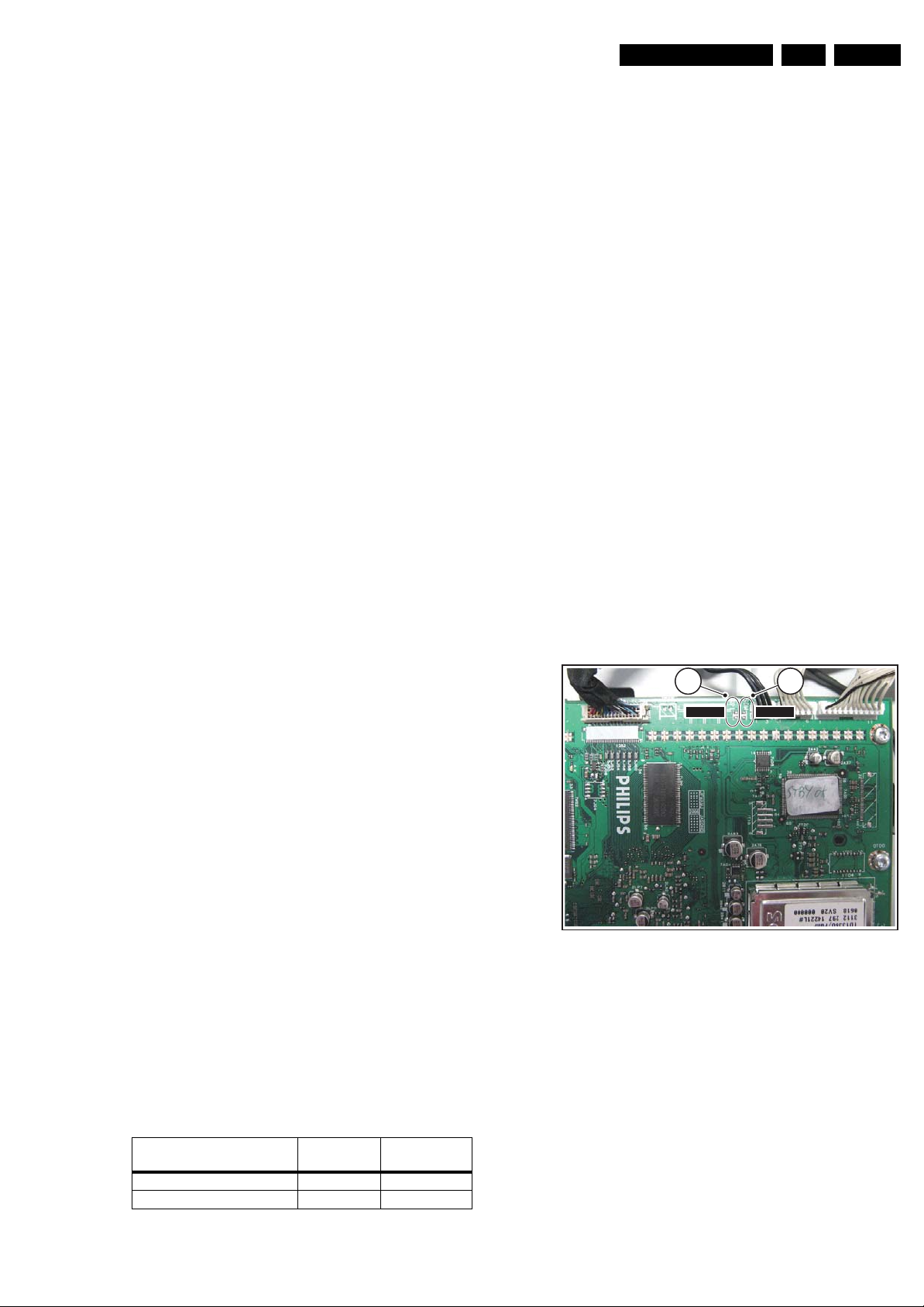
• Short for a moment the two solder pads [1] on the SSB,
with the indication “SDM”. They are located on top of the
SSB. Activation can be performed in all modes, except
when the set has a problem with the Stand-by Processor.
See figure “SDM and SPI service pads”.
12
SDMSPI
5.2.1 Service Default Mode (SDM)
Purpose
• To create a pre-defined setting, to get the same
measurement results as given in this manual.
• To override SW protections (only applicable for protections
detected by stand-by processor) and make the TV start up
to the step just before protection (a sort of automatic
stepwise start up). See paragraph “Stepwise Start Up”.
• To start the blinking LED procedure (not valid in protection
mode).
Specifications
Table 5-1 SDM default settings
Region Freq. (MHz)
Europe, AP-PAL/Multi 475.25 PAL B/G
NAFTA, AP-NTSC, LATAM 61.25 (ch. 3) NTSC M
Default
system
G_16840_014.eps
030107
Figure 5-1 SDM and SPI service pads
After activating this mode, “SDM” will appear in the upper right
corner of the screen (if you have picture).
How to Navigate
When you press the “MENU” button on the RC transmitter, the
set will toggle between the SDM and the normal user menu
(with the SDM mode still active in the background).
How to Exit SDM
Use one of the following methods:
• Switch the set to STAND-BY via the RC transmitter.
• Via a standard customer RC transmitter: key in “00”sequence.
EN 18 EJ3.0U LA5.
Service Modes, Error Codes, and Fault Finding
5.2.2 Service Alignment Mode (SAM)
Purpose
• To perform (software) alignments.
• To change option settings.
• To easily identify the used software version.
• To view operation hours.
• To display (or clear) the error code buffer.
How to Activate SAM
Via a standard RC transmitter: key in the code “062596”
directly followed by the “INFO” button. After activating SAM
with this method a service warning will appear on the screen,
you can continue by pressing the red button on the RC.
Contents of SAM:
• Hardware Info.
– A. VIPER SW Version. Displays the software version
of the VIPER software (main software) (example:
EJ30U_0.77.0.0 = AAAAB_X.Y.W.Z_NNNNN).
• AAAA= the chassis name.
• B= the region: A= AP, E= EU, L= Latam, U = US.
• X.Y.W.Z= the software version, where X is the
main version number (different numbers are not
compatible with one another) and Y is the sub
version number (a higher number is always
compatible with a lower number). The last two
digits are used for development reasons only, so
they will always be zero in official releases.
• NNNNN= last five digits of 12nc code of the
software.
– B. SBY PROC Version. Displays the software version
of the stand-by processor.
– C. Production Code. Displays the production code of
the TV, this is the serial number as printed on the back
of the TV set. Note that if an NVM is replaced or is
initialized after corruption, this production code has to
be re-written to NVM. ComPair will foresee in a
possibility to do this.
• Operation Hours. Displays the accumulated total of
operation hours (not the stand-by hours). Every time the
TV is switched "ON/OFF", 0.5 hours is added to this
number.
• Errors. (Followed by maximal 10 errors). The most recent
error is displayed at the upper left (for an error explanation
see paragraph “Error Codes”).
• Defective Module. Here the module that generates the
error is displayed. If there are multiple errors in the buffer,
which are not all generated by a single module, there is
probably another defect. It will then display the message
“UNKNOWN” here.
• Reset Error Buffer. When you press “cursor right” and
then the “OK” button, the error buffer is reset.
• Alignments. This will activate the “ALIGNMENTS” submenu.
• Dealer Options. Extra features for the dealers.
• Options. Extra features for Service.
• Initialize NVM. When an NVM was corrupted (or replaced)
in the former EMG based chassis, the microprocessor
replaces the content with default data (to assure that the
set can operate). However, all preferences and alignment
values are gone now, and option numbers are not correct.
Therefore, this was a very drastic way. In this chassis, the
procedure is implemented in another way: The moment the
processor recognizes a corrupted NVM, the “initialize
NVM” line will be highlighted. Now, you can do two things
(dependent of the service instructions at that moment):
– Save the content of the NVM via ComPair for
development analysis, before initializing. This will give
the Service department an extra possibility for
diagnosis (e.g. when Development asks for this).
– Initialize the NVM (same as in the past, however now it
happens conscious).
Note: When you have a corrupted NVM, or you have replaced
the NVM, there is a high possibility that you will not have picture
any more because your display option is not correct. So, before
you can initialize your NVM via the SAM, you need to have
picture and therefore you need the correct display option. To
adapt this option, you can use ComPair (the correct HEX
values for the options can be found in the table below) or a
method via a standard RC (described below).
Changing the display option via a standard RC:
Key in the code “062598” directly followed by the “MENU”
button and by “XXX” (where XXX is the 3 digit decimal display
option code as mentioned in the first column of the next table).
Make sure to key in all three digits, also the leading zero’s. If
the above action is successful, the front LED will go out as an
indication that the RC sequence was correct. After the display
option is changed in the NVM, the TV will go to the Stand-by
mode. If the NVM was corrupted or empty before this action, it
will be initialized first (loaded with default values). This
initializing can take up to 20 seconds.
Display Option
Code
39mm
040
PHILIPS
MODEL:
32PF9968/10
27mm
PROD.SERIAL NO:
AG 1A0620 000001
(CTN Sticker)
E_06532_038.eps
290107
Figure 5-2 Location of Display Option Code sticker

Service Modes, Error Codes, and Fault Finding
Display
HEX Display type Brand SIZE Full HDClear LCD Resolution
option
000 00 PDP SDI 42 768p 1024
001 01 PDP SDI 50 768p 1366
002 02 PDP FHP 42 1024i 1024
003 03 LCD LPL 30 768p 1280 LC300W01-A3P7 9322 198 00682
004 04 LCD LPL 37 768p 1366 LC370W 01-A6 9322 220 87682
005 05 LCD LPL 42 768p 1366 LC420W 02-A6 9322 226 39682
006 06 LCD Sharp 32 768p 1366 LQ315T3LZ13 (ASV1)
007 07 PDP SDI 42 480p 852
008 08 PDP FHP 37 1024i 1024
009 09 LCOS XION 720p 1280 n.a. n.a.
010 0A LCD AUO 30 768p 1280
011 0B LCD LPL 32 768p 1366 LC320W01-A6K1 9322 217 44682
012 0C LCD AUO 32 768p 1366 T315XW01V5 9322 231 69682
013 0D LCD Sharp 37 768p 1366 LQ370T3LZ21 (ASV2)
014 0E LCD LPL 42 X 1080p 1920 LC420WU1-SL01 9322 228 99682
015 0F PDP SDI 37 480p 852
016 10 PDP FHP 37 1080i 1024
017 11 PDP FHP 42 1080i 1024
018 12 PDP FHP 55 768p 1366
019 13 LCOS VENUS 720p 1280 n.a. n.a.
020 14 LCOS VENUS X 1080p 1920 n.a. n.a.
021 15 LCD LPL 26 768p 1366 LC260W X2-SL01 9322 221 01682
022 16 LCD LPL 32 SC BL 768p 1366 LC320WX2-SL01
023 17 PDP LGE 42 480p 852
024 18 PDP SDI 42 480p 852
025 19 PDP SDI 42 768p 1024
026 1A PDP FHP 42 1024i 1024
027 1B PDP SDI 50 768p 1366
028 1C LCD Sharp 37 X 1080p 1920 LQ370D3LZ13 (ASV2.2) 9322 228 48682
029 1D LCD AUO 32 768p 1366 T315XW01-V3 not used
030 1E LCD Sharp 37 X BDI 1080p 1920 LW 370D3LZ1x (ASV 3 first samples) not used
031 1F LCD Sharp 37 X BDI 1080p 1920 LK370D3LZ33 (ASV 3)
032 20 LCD LPL 20 768p 1366 LC200W X1-SL01 9322 222 90682
033 21 LCD QDI 23 768p 1366
034 22 ECO PTV 51 1080i 1366 ?
035 23 ECO PTV 55 1080i 1366 ?
036 24 ECO PTV 61 1080i 1366 ?
037 25 PDP FHP 42 1024I 1024
038 26 DLP 50 720p 1280 ?
039 27 DLP 60 720p 1280 ?
040 28 LCD Sharp 32 768p 1366 LK315T3LZ43 (ASV 2.3) 9322 235 32682
041 29 LCD LPL 42 SC BL 768p 1366 LC420WX2-SLA1 9322 240 80682
042 2A PDP SDI 63 768p 1366
043 2B LCD Sharp 37 BDI 768p 1366 LK370T3LZ63 (ASV 3)
044 2C LCD Sharp 37 768p 1366 LK370T3LZ53 (ASV 2.3)
045 2D LCD LPL 26 768p 1366 LC260WX2-SLB2 9322 234 13682
046 2E LCD LPL 32 768p 1366 LC320W01-SL06 9322 230 03682
047 2F LCD LPL 42 768p 1366 LC420W02-SLB1 9322 234 12682
048 30 LCD QDI 26 768p 1366 QD26HL02-REV01
049 31 LCD AUO 26 768p 1366 T260XW02V4 9322 231 90682
050 32 LCD AUO 32 768p 1366 T315XW01V9 9322 231 89682
051 33 LCD AUO 37 768p 1366 T370XW01V1 9322 233 78682
052 34 LCD AUO 32 768p 1366 T315XW02V5 not us ed
053 35 LCD LPL 37 768p 1366 LC370W X1-SL04 9322 233 19682
054 36 PDP LGE 42 768p 1024
055 37 LCD LPL 42 X 1080p 1920
056 38 LCD LPL 47 X 1080p 1920
057 39 LCD LPL 42 768p 1366
058 3A LCD LPL 42 X SC BL 1080p 1920
059 3B
060 3C LCD Sharp 37 X DFI 1080p 1920
061 3D LCD LPL 42 DFI 768p 1366
062 3E LCD LPL 32 DFI 768p 1366
063 3F LCD LPL 47 X DFI 1080p 1920
vertical
Resolution
horizontal
Type number 12 NC
S42AX-YD01(PP42AX-007A) 9322 225 38682
S50HW-XD03 9322 215 26682
FPF42C128128UC-52 (A1) 9322 212 78682
LQ315T3LZ23 (ASV2.2)(5Vtcon)
LQ315T3LZ23 (ASV2.2)(12Vtcon)
S42SD-YD05 (V3) 9322 215 27682
FPF37C128128UB-72 9322 217 56682
T296XW01
T296XW01V2
T296XW01V3
LQ370T3LZ44 (ASV2.2)
S37SD-YD02 9322 217 39682
not used not used
FPF42C128135UA-52 9322 235 43682
not used not used
not used not used
S42SD-YD07(PP42SD-015A) (V4)
S42SD-YD07(PP42SD-015B) (V4)
S42SD-YD07(PP42SD-015F) (V4)
S42AX-YD01(PP42AX-007A) (V4)
S42AX-YD01(PP42AX-008A) (V4)
S42AX-YD01(PP42AX-008B) (V4)
S42AX-YD02(PP42AX-009A) (W1)
S42AX-YD02 (PS-425-PHN) (W1)
FPF42C128128UD-51 (A2) not used
S50HW-XD04(PP50HW-005A) (V4)
S50HW-XD04(PP50HW-005B) (V4)
S50HW-XD04(PP50HW-005E) (V4)
S50HW-YD01(PP50HW -010A) (W1)
QD23HL02 REV01
QD23HL02 REV01(03)
FPF42C128135UA-52 (A3) 9322 235 43682
S63HW-XD05(1H341W) 9322 246 18682
QD26HL02-REV02
PDP42X3S000
PDP42X3V000
LC420WU2-SLA1 9322 246 84682
LC470WU1-SLC2 9322 248 50682
LC420WX3-SLA2
LC420WU5-SLA1
LK370D3LZXX
FMB reserved
WX5 SLB1
WCG
9322 209 35682
9322 226 58682
9322 226 16682
9322 206 49682
9322 219 45682
9322 213 33682
?
9322 241 46682
9322 226 37682
9322 226 96682
9322 233 81682
9322 225 38682
9322 226 95682
9322 233 80682
9322 240 08682
9322 242 85682
9322 226 54682
9322 226 97682
9322 233 79682
9322 240 25682
9322 242 22682
9322 223 91682
9322 232 69682
9322 247 94682
9322 235 83682
9322 227 29682
9322 235 05682
9322 245 29682
9322 246 93682
under development
under development
reserved
under development
under development
under development
E_06532_030a.eps
EN 19EJ3.0U LA 5.
080207
Figure 5-3 Display option code overview [1/2] (for all Philips FTV chassis)
EN 20 EJ3.0U LA5.
Display
option
064 40
065 41
066 42 PDP SDI 63 x 1080p 1920
067 43 LCD AUO 26 768p 1366
068 44 LCD CMO 26 768p 1366
069 45 LCD CMO 32 768p 1366
070 46 LCD CPT 32 768p 1366
071 47 LCD LPL 37 768p 1366
072 48 LCD AUO 37 768p 1366
073 49 LCD LPL 42 768p 1366
074 4A LCD LPL 42 DFI 768p 1366
075 4B LCD Sharp 52 X DFI 1080p 1920
076 4C LCD AUO 42 768p 1366
077 4D LCD AUO 42 BDI 768p 1366
078 4E LCD AUO 42 X 1080P 1920
079 4F LCD CMO 42 BDI 768p 1366
080 50 LCD CMO 42 X 1080P 1920
081 51 LCD LPL 47 X 1080P 1920
082 52 LCD AUO 47 X 1080P 1920
083 53 PDP SDI 42 768p 1024
084 54 PDP LGE 42 768p 1024
085 55 PDP SDI 50 768p 1366
086 56 PDP LGE 50 768p 1366
087 57 LCD Sharp 37 X BDI 1080p 1920
088 58 LCD Sharp 37 BDI 768P 1366
089 59 LCD AUO 42 768p 1366
090 5A LCD AUO 26 768p 1366
091 5B LCD AUO 32 768P 1366
092 5C LCD LPL 42 768p 1366 LC420WX2-SLA1 9322 240 80682
093 5D LCD LPL 42 X 1080p 1920
094 5E PDP SDI 63 x 1080p 1920
095 5F LCD Sharp 37 X 1080p 1920
096 60 LCD LPL 42 X SC BL DFI 1080p 1920
097 61 LCD LPL 47 X SC BL 1080p 1920
098 62 LCD Sharp 52 X 1080p 1920
099 63
100 64 LCD 42 X 1080p 1920
101 65
102 66 LCD Sharp 32 DFI 768p 1366
103 67 LCD LPL 20 480p 640
104 68 LCD AUO 20 600p 800
105 69 LCD CMO 19 900p 1440
106 6A LCD AUO 23 768p 1366
107 6B LCD LPL 42 768P 1366
Service Modes, Error Codes, and Fault Finding
HEX Display type Brand SIZE Full HDClear LCD Resolution
vertical
Resolution
horizontal
Type number 12 NC
reserved
reserved
S63HW-YD02 (W2)
T260XW03V1
V260B1-L03 9322 249 37682
V315B1 L05 9322 248 65682
CLLAA320WB02P
LC370WX1-SLB1 9322 246 96682
T370XW02V5 9322 249 77682
LC420WX3-SLA1 9322 246 97682
LC420WX4-SLA1
LK520D3LZ1X under development
T420XW01V8 9322 249 10682
T420XW
T420HW01 V0
V420B1
V420H1
LC470WU4-SLA2
T470HW01 V0
S42AX-YD04(PS-426-PH) 9322 246 76682
HD X4
S50HW-YD05(PS-506-PH) 9322 246 81682
HD X4
LK370D3LZ43 (ASV3.0) 9322 248 28682
(ASV2,3 VE1)
T420XW01V5
T260XW03V1
T315XW02VD 9322 249 06682
LC420WU2-SLA1 9322 246 84682
S63HW-YD02 (W2) used with JIP panel
LK370D3LZ23 9322 249 96682
TBD
LC470WU6 - SLA1 under development
LK520D3LZ1X
3D
LK315T3LZ53 under developm ent
LC201V02-SDB1
A201SN02 V5
TPM190A1-L02 9965 000 43654
T230XW01V3
LC420WX5-SLD1
under development
under development
9322 245 31682
under development
under development
under development
under development
under development
under development
under development
under development
under development
under development
under development
under development
under development
under development
under development
reserved
under development
reserved
9322 242 65682
not in ECM2
9322 249 79682
9322 249 09682
E_06532_030b.eps
080207
Figure 5-4 Display option code overview [2/2] (for all Philips FTV chassis)
• Store. All options and alignments are stored when
pressing “cursor right” and then the “OK” button
• SW Maintenance.
– SW Events. Not useful for service purposes. In case of
specific software problems, the development
department can ask for this info.
– HW Events. Not functional at the moment this manual
is released, description will be published in an update
manual if the function becomes available.
• Upload to USB. Write the channel list and the settings to
a USB device.
• Download from USB. Retrieve the channel list and the
settings from a USB device.
How to Navigate
• In SAM, you can select the menu items with the “CURSOR
UP/DOWN” key on the RC transmitter. The selected item
will be highlighted. When not all menu items fit on the
screen, move the “CURSOR UP/DOWN” key to display the
next/previous menu items.
• With the “CURSOR LEFT/RIGHT” keys, it is possible to:
– (De)activate the selected menu item.
– (De)activate the selected submenu.
How to Exit SAM
Use one of the following methods:
• Press the “MENU” button on the RC transmitter.
• Switch the set to STAND-BY via the RC transmitter.
Note: As long as SAM is activated, it is not possible to change
a channel. This could hamper the White Point alignments
because you cannot choose your channel/frequency any more.
Workaround: after you have sent the RC code “062596 INFO”
you will see the service-warning screen, and in this stage it is
still possible to change the channel (so before pressing the
“OK” button).

Service Modes, Error Codes, and Fault Finding
EN 21EJ3.0U LA 5.
5.2.3 Customer Service Mode (CSM)
Purpose
When a customer is having problems with his TV-set, he can
call his dealer or the Customer Helpdesk. The service
technician can then ask the customer to activate the CSM, in
order to identify the status of the set. Now, the service
technician can judge the severity of the complaint. In many
cases, he can advise the customer how to solve the problem,
or he can decide if it is necessary to visit the customer.
The CSM is a read only mode; therefore, modifications in this
mode are not possible.
How to Activate CSM
Key in the code “123654” via the standard RC transmitter.
Note: Activation of the CSM is only possible if there is no (user)
menu on the screen!
How to Navigate
By means of the “CURSOR-DOWN/UP” knob on the RC
transmitter, you can navigate through the menus.
Contents of CSM
• CSM 1
– 1.3. Set type: Model number of the set. This
information is very helpful for a helpdesk/workshop as
reference for further diagnosis. In this way, it is not
necessary for the customer to look at the rear of the
TV-set. (*)
– 1.4. Production Code: Displays the production code
(the serial number) of the TV. (*)
– 1.5. Code 1: Gives the latest five errors of the error
buffer. As soon as the built-in diagnose software has
detected an error, the buffer is adapted. The last
occurred error is displayed on the leftmost position.
Each error code is displayed as a 2-digit number.
When less than 10 errors occur, the rest of the buffer is
empty (00). See also paragraph Error Codes for a
description.
– 1.6. Code 2: Displays the 2nd part of the error buffer.
See also paragraph Error Codes for a description.
– 1.7. Options 1: Gives the option codes of option group
1 as set in SAM (Service Alignment Mode).
– 1.8. Options 2: Gives the option codes of option group
2 as set in SAM (Service Alignment Mode).
– 1.13. 12NC SSB: Indication of the SSB order code. (*)
– 1.13. Install date: This shall be filled in after time
extraction (triggered by disabling of virgin mode, so
first time customer does channel installation). Time
extraction is done via, teletext for Europe, PBS Public
Broadcast Channels for US. This, to determine exactly
the garanty period for call centers.
• CSM 2:
– 2.2. Pixel Plus: Gives an indication if PixelPlus is set
“ON” or “OFF”.
– 2.4. DNR. Gives the selected DNR setting (Dynamic
Noise Reduction), “OFF”, “MINIMUM”, “MEDIUM”, or
“MAXIMUM”. Change via “MENU”, “TV”, “PICTURE”,
“DNR”
– 2.5. Noise Figure. Gives the noise ratio for the
selected transmitter. This value can vary from 0 (good
signal) to 127 (average signal) and to 255 (bad signal).
For some software versions, the noise figure will only
be valid when “Active Control” is set to “medium” or
“maximum” before activating CSM.
• CSM 3:
–
3.1. Headphone Volume: Gives the last status of the
headphone volume, as set by the customer. The value
can vary from 0 (volume is minimum) to 100 (volume is
maximum). Change via ”MENU”, “TV”, “SOUND”,
“HEADPHONE VOLUME”.
– 3.2. Dolby: Indicates whether the received transmitter
transmits Dolby sound (“ON”) or not (“OFF”). Attention:
The presence of Dolby can only be tested by the
software on the Dolby Signaling bit. If a Dolby
transmission is received without a Dolby Signaling bit,
this indicator will show “OFF” even though a Dolby
transmission is received.
– 3.3. Surround Mode: Indicates the by the customer
selected sound mode (or automatically chosen mode).
Possible values are “STEREO” and “VIRTUAL DOLBY
SURROUND”. Change via “MENU”, “TV”, “SOUND”,
“SOUND MODE”. It can also have been selected
automatically by signaling bits (internal software).
– 3.4. Center Input: Not applicable.
– 3.5. Audio System: Gives information about the
audible audio system. Possible values are “Stereo”,
”Mono”, “Mono selected”, “Analog In: No Dig. Audio”,
“Dolby Digital 1+1”, “Dolby Digital 1/0”, “Dolby Digital 2/
0”, “Dolby Digital 2/1”, “Dolby Digital 2/2”, “Dolby Digital
3/0”, “Dolby Digital 3/1”, “Dolby Digital 3/2”, “Dolby
Digital Dual I”, “Dolby Digital Dual II”, “MPEG 1+1”,
“MPEG 1/0”, “MPEG 2/0”. This is the same info as you
will see when pressing the “INFO” button in normal
user mode (item “signal”). In case of ATSC receiving
there will be no info displayed.
– 3.6. AVL: Indicates the last status of AVL (Automatic
Volume Level): “ON” or “OFF”. Change via “MENU”,
“TV”, “SOUND”, “AVL”. AVL can not be set in case of
digital audio reception (e.g. Dolby Digital or AC3)
– 3.7. Delta Volume: Indicates the last status of the
delta volume for the selected preset as set by the
customer: from “-12” to “+12”. Change via “MENU”,
“TV”, “SOUND”, “DELTA VOLUME”.
• CSM 4:
– 4.1. Preset Lock. Indicates if the selected preset has
a child lock: “LOCKED” or “UNLOCKED”. Change via
“MENU”, “TV”, “CHANNELS”, “CHANNEL LOCK”.
– 4.3. Lock After: Indicates at what time the channel
lock is set: “OFF” or e.g. “18:45” (lock time). Change
“MENU”, “TV”, “CHANNELS”, “LOCK AFTER”.
– 4.6. TV Ratings Lock: Indicates the “TV ratings lock”
as set by the customer. Change via “MENU”, “TV”,
“CHANNELS”, “TV RATINGS LOCK”. Possible values
are: “ALL”, “NONE”, “TV-Y”, “TV-Y7”, “TV-G”, “TV-PG”,
“TV-14” and “TV-MA”.
– 4.7. Movie Ratings Lock: Indicates the “Movie ratings
lock” as set by the customer. Change via “MENU”,
“TV”, “CHANNELS”, “MOVIE RATINGS LOCK”.
Possible values are: “ALL”, “NR”, “G”, “PG”, “PG-13”,
“R”, “NC-17” and “X”.
– 4.8. V-Chip TV Status: Indicates the setting of the V-
chip as applied by the selected TV channel. Same
values can be shown as for “TV RATINGS LOCK”.
– 4.9. V-Chip Movie Status: Indicates the setting of the
V-chip as applied by the selected TV channel. Same
values can be shown as for “MOVIE RATINGS LOCK”.
– 4.10. Region rating Status (RRT): OFF.
• CSM 5:
–
5.1. On timer: “OFF” or “ON”.
– 5.2. Location: Gives the last status of the location
setting as set via the installation menu. Possible values
are “Shop” and “Home”. If the location is set to “Shop”,
several settings are fixed. So for a customer, location
must be set to “Home”. Can be changed via the
installation menu (see also DFU).
• CSM 6:
– 6.1. HDMI key validity: Indicates the key’s validity.
– 6.2. IEEE key validity: Indicates the key’s validity
(n.a.).
– 6.3. POD key validity: Indicates the key’s validity
(n.a.).

EN 22 EJ3.0U LA5.
Service Modes, Error Codes, and Fault Finding
• CSM 7:
– 7.2. TV System: Gives information about the video
system of the selected transmitter.
a. M: NTSC M signal received.
b. ATSC: ATSC signal received.
– 7.3. Source: Indicates which source is used and the
video/audio signal quality of the selected source.
(Example: Tuner, Video/NICAM) Source: “TUNER”,
“AV1”, “AV2”, “AV3”, “HDMI 1”, “SIDE”. Video signal
quality: “VIDEO”, “S-VIDEO”, “RGB 1FH”, “YPBPR
1FH 480P”, “YPBPR 1FH 576P”, “YPBPR 1FH 1080I”,
“YPBPR 2FH 480P”, “YPBPR 2FH 576P”, “YPBPR
2FH 1080I”, “RGB 2FH 480P”, “RGB 2FH 576P” or
“RGB 2FH 1080I”. Audio signal quality: “STEREO”,
“SPDIF 1”, “SPDIF 2”, or “SPDIF”.
– 7.4. Tuned Bit: Indicates if the selected preset is
automatically tuned (via “Automatic Installation” in the
setup menu) or via the automatic tuning system of the
TV. In this case “Tuned bit” will show “YES”. If the TV
was not able to auto-tune to the correct frequency, this
item will show “NO”. So if “NO” is displayed, it could
indicate that the customer has manually tuned to a
frequency which was too far from a correct frequency,
that the TV was not able to auto-tune any more.
– 7.6. Digital Signal Modulation: Indicates quality of
the received digital signal (0 = low).
• CSM 8:
– 8.1. 12NC one zip SW: Displays the 12NC number of
the one-zip file as it is used for programming software
in production. In this one-zip file all below software
version can be found.
– 8.2. Initial Main SW: Displays the main software
version which was initially loaded by the factory.
– 8.3. Current Main SW: Displays the built-in main
software version. In case of field problems related to
software, software can be upgraded. As this software
is consumer upgradeable, it will also be published on
the Internet. E.g. EJ30U_0.77.0.0.
– 8.5. Flash Utils SW: Displays the software version of
the software which contains all necessary components
of the download application. To program this software,
EJTAG tooling is needed.E.g. EJ30U_0.77.0.0.
– 8.6. Standby SW: Displays the built-in stand-by
processor software version. Upgrading this software
will be possible via ComPair or via USB.(see chapter
Software upgrade). E.g. STDBY_3.0.1.37.
– 8.7. MOP SW: Displays the MOP software version.
E.g. RXS3E_2.3.0.0.
– 8.8. Pacific 3 Flash SW: Displays the Pacific 3
software version. E.g. P3FW0_1.6.2.0
– 8.11. NVM version: Displays the NVM version as
programmed by factory. E.g. EJ30U_0.0.0.4
The abbreviations “SP” and “MP” in the figures stand for:
• SP: protection or error detected by the Stand-by
Processor.
• MP: protection or error detected by the VIPER Main
Processor.
How to Exit CSM
Press any key on the RC transmitter (with exception of the
“CHANNEL +/-”, “VOLUME”, “MUTE” and digit (0-9) keys).
5.3 Stepwise Start-up
The stepwise start-up method, as known from FTL/FTP sets is
not valid any more. The situation for this chassis is as follows:
when the TV is in a protection state detected via the Stand-by
Processor (and thus blinking an error) and SDM is activated via
short cutting the pins on the SSB, the TV starts up until it
reaches the situation just before protection. So, this is a kind of
automatic stepwise start-up. In combination with the start-up
diagrams below, you can see which supplies are present at a
certain moment.
Important to know here is, that if e.g. the 3V3 detection fails
(and thus error 11 is blinking) and the TV is restarted via SDM,
the Stand-by Processor will enable the 3V3, but will not go to
protection now. The TV will stay in this situation until it is reset
(Mains/AC Power supply interrupted).
Service Modes, Error Codes, and Fault Finding
Off
Mains
“off”
Mains
“on”
EN 23EJ3.0U LA 5.
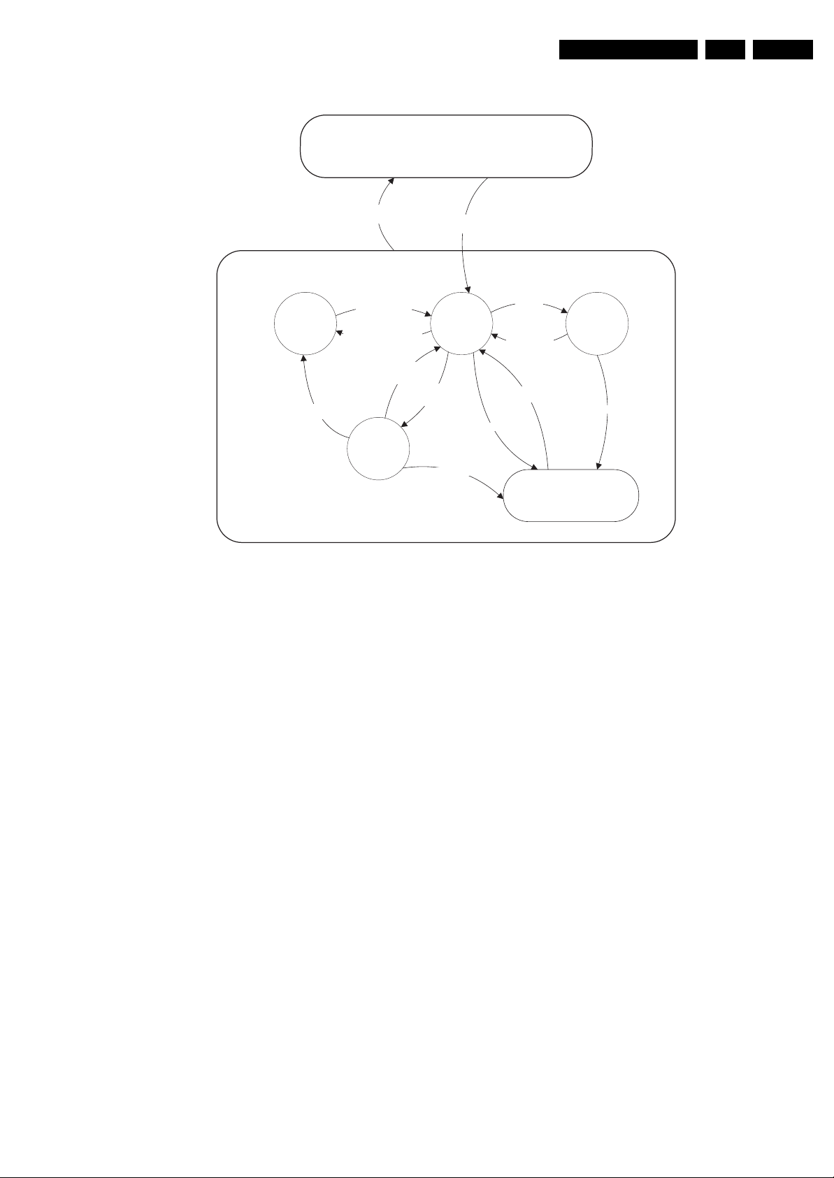
- WakeUp requested
- Acquisition needed
Stand-by
(Off St-by)
- POD Card remove
- Tact SW pushed
- No data Acquisition required
and no POD present
- Tact SW pushed
- WakeUp requested
- Acquisition needed
d
POD
Stand-by
On
Only applicable for sets with CableCARDTM slot (POD)
*
Figure 5-5 Transition diagram
No data Acquisition
required and
POD present
*
Semi
Stand-by
GoToProtection
GoToProtec
tion
WakeUp
requested
- St-by requested
- Tact SW pushed
WakeUp
requested
Protection
Active
GoToProtection
F_15400_095.eps
020206
EN 24 EJ3.0U LA5.
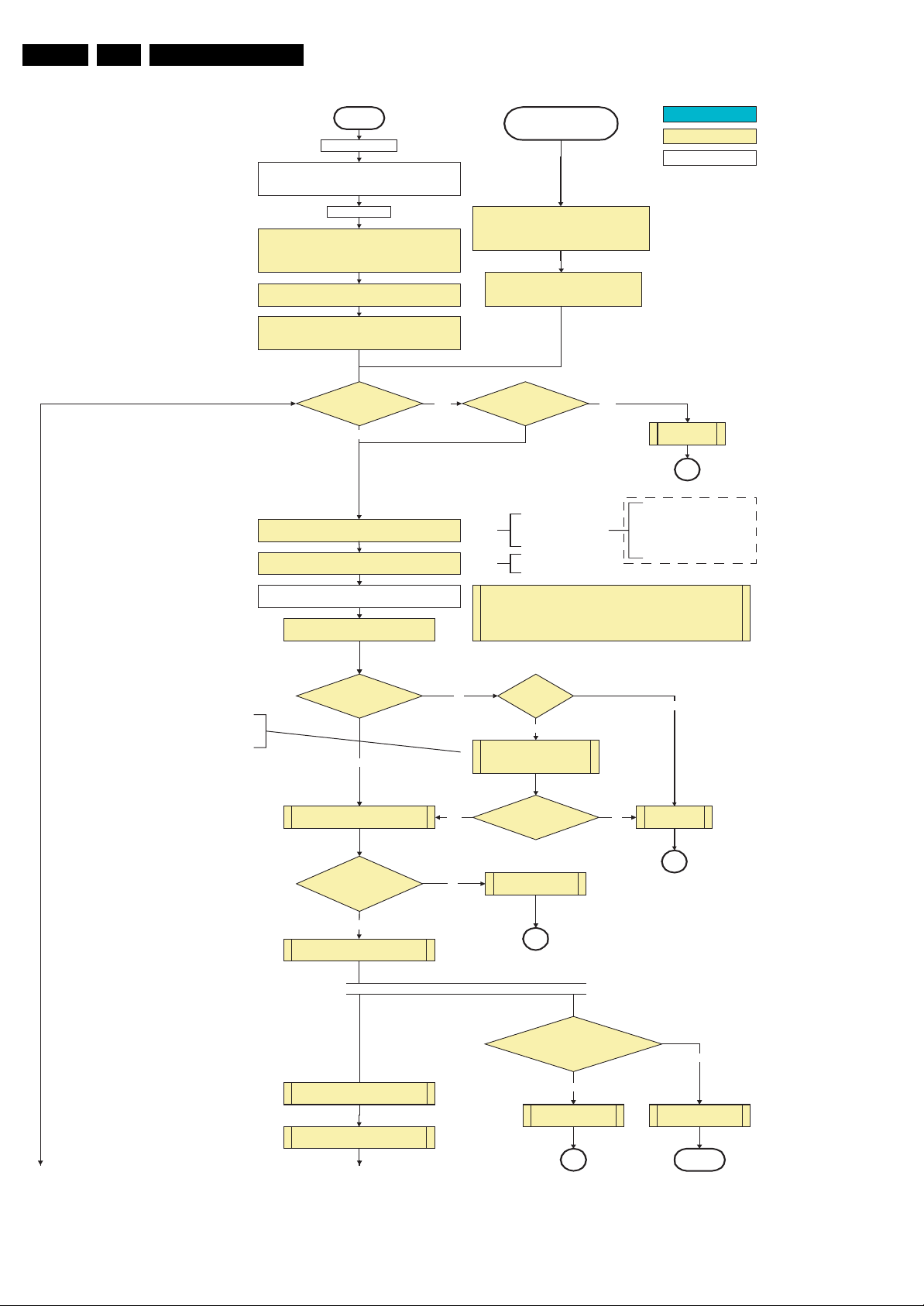
Service Modes, Error Codes, and Fault Finding
Off
Mains is applied
Standby Supply starts running.
+5V2, 1V2Stb, 3V3Stb and +2V5D become present.
In case of PDP 3V3 Vpr to CPU PDP becomes present.
st-by µP resets
All I/O lines have a “high” default state:
- Assert the Viper reset.
- Sound-Enable and Reset-Audio should remain “high”.
- NVM power line is “high”, no NVM communication possible.
Initialise I/O pins of the st-by µP, start keyboard scanning, RC
detection, P50 decoding. Wake up reasons are “off”.
In case of FHP PDP: Switch PDPGO “low”
CPUGO (inverse of the stby I/O line POD-MODE) and PDPGO
are then both “low” and the PDP is in the “low power” mode.
ECO Baby Jaguar??
No
Switch “low” the NVM power reset line. Add a 2ms delay
before trying to address the NVM to allow correct NVM
Switch “on” all supplies by switching LOW the POD-MODE
+5V, +8V6, +12VS, +12VSW and Vsound are switched on
Wait 50ms and then star t polling the detect-
5V, detect-8V6 and detect-12V every 40ms.
initialization.
and the ON-MODE I/O lines.
Yes Yes
Stand-by or
Protection
If the protection state was left by short circuiting the
SDM pins, detection of a protection condition during
startup will stall the startup. Protection conditions in a
playing set will be ignored. The protection mode will
- Switch Sound-Enable and Reset-Audio “high”.
not be entered.
They are “low” in the standby mode if the
standby mode lasted longer than 2s.
*
Auto Protection
Line High??
Switching the POD-MODE and the
Switching the POD-MODE
low in an FHP PDP set
makes the CPUGO go “high”
and starts the PDP CPU.
except in an FHP PDP Cold
Boot
“on” mode “low” in an SDI PDP set
makes the PDP supplies go to the
*
“on” mode. Within 4 seconds, a
valid LVDS must be sent to the
display to prev ent protection.
(valid for V3 version)
*
The availab ility of the supplies is che cked through detect signals (delivered by
dedicated detect-IC's) going to the st-by µP. These signals are available for
+12V, +8V6, +5V, +1V2 and +2V5. A low to high transition of the signals should
occur within a certain time after toggling the standby line. If an observers is
detected before the time-out elapses, of course, the process should continue in
order to minimize start up time.
action holder: MIPS
action holder: St-by
autonomous action
Audio Error
SP
*
detect-5V
received within
2900 ms after POD-MODE
Switching the PDPGO “high”
will give a visual artefa ct and
should only be done if really
necessary.
activate +5V supply detection algorithm
Enable the +1V2 supply (ENABLE-1V2)
Start polling the detect-1V2 every 40ms
To part B To part B
Only applicable for sets with CableCARD
*
TM
slot (POD)
toggle?
Yes
detect-12VSW received within
2900 ms after POD-mode
toggle?
Yes
activate +12VSW supply
detection algorithm
*
No
Yes
No
FHP PDP Set?
Yes
Switch PDPGO high :
PDP should start: 5V, 8V6 and
12V are activated
detect-5V
received within
2900 ms after PDPGO
toggle?
+12V error
SP
No need to wait for the 8V6 detection at this point.
within 6300 ms after POD-mode toggle?
Startup shall not wait for this detection
detect-8V6 received
and continue startup.
No
+8V6 erro r
SP
No
+5V error
No
SP
*
Yes
activate +8V6 supply
detection algorithm
return
F_15400_096a.eps
230606
Figure 5-6 “OFF” to “Semi Stand-by” flowchart (part 1)

Service Modes, Error Codes, and Fault Finding
EN 25EJ3.0U LA 5.
From part A
No
From part B
detect-1V2
received within
250ms?
Yes
Enable the supply for
+2.5V and +3.3V (ENABLE-3V3)
Start polling the detect-3V3 every 40ms
detect-3V3
received within
250 ms?
Yes
Activate supply detection algorithms for
+1V2 and +3V3
SUPPLY-FAULT I/O line
is High?
Yes
Enable the supply fault detection
interrup t
action holder: MIPS
action holder: St-by
autonomous action
No
+1.2V error
SP
No separate enable and
detect is present for the +2V5
supply in the Baby Jaguar.
+3.3V errorNo
SP
Supply fault errorNo
SP
No
No
Release viper reset
Feed warm boot script(2)
Set I²C slave address
of Standby µP to (A0h)
Detect EJTAG debug probe
(pulling pin of the probe interface to
ground by inserting EJTAG probe)
EJTAG pro be
connected ?
No
Cold boot?
Yes
Release viper reset
Feed cold boot script(1)
Release PNX2015 reset 100ms after
Viper reset is released
Bootscript ready
in 1250 ms?
Yes
Set I²C slave address
of Standby µP to (64h)
RPC start (comm. protocol)
Yes
Release viper reset
Feed initializing boot script (3)
disable alive mechanism
Release PNX2015 reset 100ms
after Viper reset is released
No
Flash to RAM image
transfer succeeded
within 30s?
Yes
Viper SW initialization
succeeded
within 20s?
Code = 5
Switch Viper in reset
No
Code = 53
To part C To part C To part C To part C
F_15400_096b.eps
Figure 5-7 “OFF” to “Semi Stand-by” flowchart (part 2)
260505

EN 26 EJ3.0U LA5.
Service Modes, Error Codes, and Fault Finding
From part B From part B From part B
Yes
Enable Alive check mechanism
MIPS reads the wake up reason
from standby µP.
SDI PDP
Set?
No
FHP PDP
Set?
Switch “on” the LVDS output of
*
the PNX2015 with a correct
clock frequency within 4s after
Yes
switching the POD and “on”
mode to prevent PDP display
supply protection.
These LVDS items are
SDI V3 displ ay only ! !
Yes
Send ST BYEN = 1
to PDP displ ay (I²C)
PFCON = 1
VCCON = 1
Wait until Viper starts to
communicate
3-th try?
Yes
Log Code as
error code
SP
Wait 10ms
Switch the NVM reset
line HIGH.
Disable all supply related protections and
switch off the +2V5, +3V3 DC/DC converter.
Wait 5ms
switch off the remaining DC/DC
converters
Switch POD- MODE an d ON-MODE
I/O line “high”.
*
Wait for the +8V6 to be detected if not yet present. (if
it does not come, the standby µP will enter a
protection mode, this is not a dead end here)
PWR-OK- PDP
received within 10s
after POD and “on” mode
toggle ?
Yes
Init SDI PDP
Switch LVDS back off if
end state is not the active
state.
Switch PDPGO “ low”
*
action holder: MIPS
action holder: St-by
autonomous action
No
Log display
error and enter
protection mode
SP
No
Start 4 seconds preheating timer in case of
a LPL scanning backlight LCD set.
AVIP needs to be started before the MPIF in order to have a good clock distribution.
AVIP default power-up mode is Standby. The Viper instructs AVIP via I²C to enable all the
PLLs and clocks and hence enter to Full Power mode.
Initialize PNX2015 HD subsystem
MPIFs should be initialized
MPIF should deliver 4 observers:
POR= 0; normal operation
MSUP = 1: Main supply is present
ASUP = 1; audio supply is present
ROK = 1; reference frequency is present (coming from AVIP)
All observers present with correct state?
Yes
Initialize tuners and HDMI
Initialize source selectio n
Initialize video processing ICs
- Spider (if available)
No
Init FHP PDP
Log appropriate
Observer error
Do not enter semi-standby state in case of an LPL
scanning backlight LCD set before 4 s preheating timer has
elapsed.
Only applicable for sets with CableCARDTM slot (POD)
*
Figure 5-8 “OFF” to “Semi Stand-by” flowchart (part 3)
Initialize Columbus
Initialize 3D Combfilt er
Initialize AutoTV
Semi-Stand-by
F_15400_096c.eps
020206
Service Modes, Error Codes, and Fault Finding
EN 27EJ3.0U LA 5.
action holder: MIPS
action holder: St-by
autonomous action
26" /32" / 37" / 42" LCD LPL
Semi Standby
Wait until previous on-state is left more than 2
seconds ago. (to prevent LCD display problems)
Assert RGB video blanking
and audio mute
Initialize audio and video processing ICs and
functions according needed use case.
Wait until QVCP generates a valid LVDS output
clock.
Switch “on” 12V LCD supply
(LCD-Power-on)
Start to apply valid interface signals to the module (LVDS) within a time
frame of min. 17.5ms to max. 67.5ms after supply switch “on”.
In implementation, use 25ms, this makes it compatible with 37HD"Sharp
(t=17.5ms is the supply switch-on delay taken into account)
Wait 250ms (min. = 200ms)
Switch “off” RGB blanking
Switch “on” LCD lamp after valid, stable video, corresponding
to the requested output is delivered by the Viper
Switch Audio-Reset and sound enable “low” and demute
Active
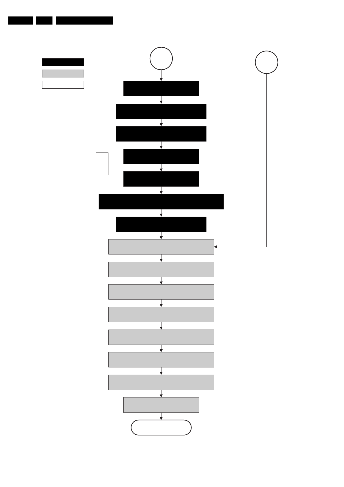
Figure 5-9 “Semi Stand-by” to “Active” flowchart
G_16290_079.,eps
020206
EN 28 EJ3.0U LA5.
Service Modes, Error Codes, and Fault Finding
26" /32" / 37" / 42" LCD LPL
action holder: MIPS
Active
Mute all sound outputs.
Switch reset-audio and sound-enable
lines “high”.
Switch “off” LCD lamp.
Mute all video outputs.
Wait 250ms (min. = 200ms).
action holder: St-by
autonomous action
Switch “off” LVDS signal
(Viper I/O: PD-LVDS).
Switch “off” 12V LCD supply within a time frame of min.
0.5 ms to max. 50ms after LVDS switch “off”.
(Viper I/O: LCD_PWR_ON).
Semi Standby
Figure 5-10 “Active” to “Semi Stand-by” flowchart
G_16290_080.eps
020206

Service Modes, Error Codes, and Fault Finding
EN 29EJ3.0U LA 5.
*
POD
Transfer Wake up reasons to the
Images are re-transferred to DDR-RAM from
Flash RAM (verification through checksum).
MIPS image completes the application reload,
stops DDR-RAM access, puts itself in a
sleepmode, and signals the standby µP when
the Stand-by mode can be entered.
DDR-RAM is put in self refresh mode and the images
are kept in the hibernating DDR-RAM.
Stand- by µP.
Wait 5ms
Semi Stand-by
action holder: MIPS
action holder: St-by
autonomous action
Important remark:
release RESET AUDIO and
SOUND_ENABLE 2 sec after
entering stand-by to save power
Switch Viper in reset state
Wait 10ms
Switch the NVM reset line “high”.
Disable all supply related protections and switch “off”
the +2V5, +3V3 DC/DC converter.
Wait 5ms
Switch “off” the remaining DC/DC converters
Switch “off” all supplies by switching “high” the POD-
MODE and the ON-MODE I/O lines.
*
For PDP this means
CPUGO becomes low.
Only applicable for sets with CableCARDTM slot (POD)
*
Figure 5-11 “Semi Stand-by” to “Stand-by” flowchart
Stand-by
F_15400_099.eps
020206
EN 30 EJ3.0U LA5.
Service Modes, Error Codes, and Fault Finding
action holder: MIPS
action holder: St-by
autonomous action
If needed to speed up this transition,
this block could be omitted. This is
depending on the outcome of the
safety investigations.
min. 0.5ms to max. 50ms after LVDS switch “off”. (for LCD sets)
MP
Log the appropriate error and
set stand-by flag in NVM
Redefine wake up reasons for protection
state and transfer to stand-by µP.
Switch “off” LCD lamp supply (for LCD sets)
Wait 250ms (min. = 200ms)
Switch “off” LVDS signal
Switch “off” 12V LCD supply within a time frame of
Ask stand-by µP to enter protection state
SP
Switch Viper in reset state
Wait 10ms
Switch the NVM reset line “high”.
Disable all supply related protections and switch “off”
the +2V5, +3V3 DC/DC converter.
Wait 5ms
Switch “off” the remaining DC/DC converters
Switch “off” all supplies by switching “high” the POD-
MODE and the ON-MODE I/O lines.
Flash LED in order to indicate
protection state.
*
Only applicable for sets with CableCARDTM slot (POD)
*
Figure 5-12 “Protection” flowchart
Protection
F_15400_102.eps
020206
 Loading...