

Philips BFQ251A, BFQ251 Datasheet

DATA SH EET
Product specification
Supersedes data of 1997 Oct 02
1998 Oct 06
DISCRETE SEMICONDUCTORS
BFQ251
PNP video transistor
ook, halfpage
M3D186
1998 Oct 06 2
Philips Semiconductors Product specification
PNP video transistor BFQ251
FEATURES
• High breakdown voltages
• Low output capacitance
• High gain bandwidth
• Good thermal stability
• Gold metallization ensures
excellent reliability.
APPLICATIONS
• Buffer/driver in high-resolution
colour graphics monitors.
DESCRIPTION
PNP video transistor in a SOT54
(TO-92) plastic package.
NPN complement: BFQ231.
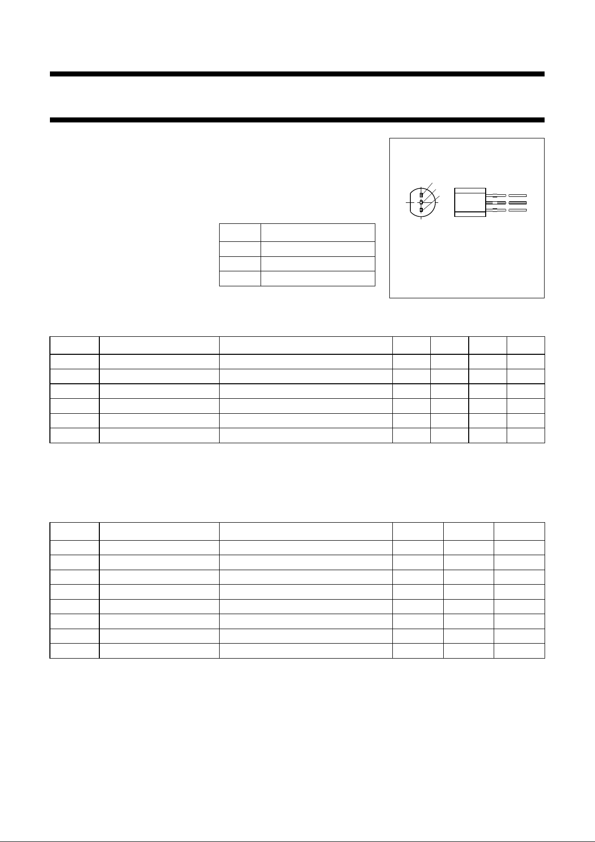
PINNING
PIN DESCRIPTION
1 base
2 collector
3 emitter
Fig.1 Simplified outline
(SOT54; TO-92).
age
1
3
2
MSB033
QUICK REFERENCE DATA
Note
1. T
s
is the temperature at the soldering point of the collector pin, 4 mm from the body.
LIMITING VALUES
In accordance with the Absolute Maximum Rating System (IEC 134).
Notes
1. T
s
is the temperature at the soldering point of the collector pin, 4 mm from the body.
2. Transistor mounted on a printed-circuit board with a metallized pad area of 10 mm2.
SYMBOL PARAMETER CONDITIONS MIN. TYP. MAX. UNIT
V
CBO
collector-base voltage open emitter −−−100 V
V
CER
collector-emitter voltage RBE= 100 Ω −−−95 V
I
C
collector current (DC) −−−300 mA
P
tot
total power dissipation Ts≤ 65 °C; note 1 −−1W
h
FE
DC current gain IC= −50 mA; VCE= −10 V 20 30 −
f
T
transition frequency IC= −50 mA; VCE= −10 V; T
amb
=25°C 1 1.3 − GHz
SYMBOL P ARAMETER CONDITIONS MIN. MAX. UNIT
V
CBO
collector-base voltage open emitter −−100 V
V
CEO
collector-emitter voltage open base −−65 V
V
CER
collector-emitter voltage RBE= 100 Ω−−95 V
V
EBO
emitter-base voltage open collector −−3V
I
C
collector current (DC) −−300 mA
P
tot
total power dissipation Ts≤ 65 °C; notes 1 and 2; see Fig.3 − 1W
T
stg
storage temperature −65 +150 °C
T
j
junction temperature − 150 °C
1998 Oct 06 3
Philips Semiconductors Product specification
PNP video transistor BFQ251
THERMAL CHARACTERISTICS
Note
1. Ts is the temperature at the soldering point of the collector pin, 4 mm from the body.
CHARACTERISTICS
T
j
=25°C unless otherwise specified.
SYMBOL PARAMETER CONDITIONS VALUE UNIT
R
th j-s
thermal resistance from junction to soldering point note 1 85 K/W
R
th j-a
thermal resistance from junction to ambient 185 K/W
SYMBOL PARAMETER CONDITIONS MIN. TYP. MAX. UNIT
V
(BR)CBO
collector-base breakdown voltage IC= −0.1 mA; IE=0 −100 −−V
V
(BR)CEO
collector-emitter breakdown voltage IC= −10 mA; IB=0 −65 −−V
V
(BR)CER
collector-emitter breakdown voltage IC= −10 mA; RBE= 100 Ω−95 −−V
V
(BR)EBO
emitter-base breakdown voltage IE= −0.1 mA; IC=0 −3 −−V
I
CES
collector-emitter cut-off current IB= 0; VCE= −50 V −−−100 µA
I
CBO
collector-base cut-off current IE= 0; VCB= −50 V −−−20 µA
h
FE
DC current gain IC= −50 mA; VCE= −10 V; see Fig.4 20 30 −
C
cb
collector-base capacitance IC=ic= 0; VCB= −10 V; f = 1 MHz;
see Fig.5
− 2 − pF
f
T
transition frequency IC= −50; VCE= −10 V; see Fig.6 1 1.3 − GHz
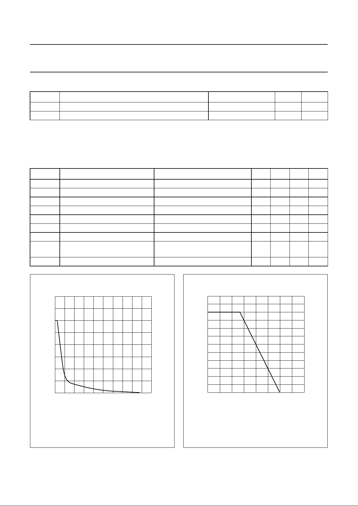
Fig.2 DC SOAR.
T
amb
=25°C.
handbook, halfpage
0 −40 −100
−400
−300
−100
0
−200
MEA232 - 1
−20 −60 −80
I
C
(mA)
V
CEO
(V)
Fig.3 Power derating curve.
handbook, halfpage
0 50 100 200
0.8
0.6
0.2
0
0.4
MEA228 - 1
150
1.0
1.2
Ts (oC)
P
tot
(W)
 Loading...