

Philips BFQ235A Datasheet
DISCRETE SEMICONDUCTORS
DATA SH EET
M3D066
BFQ235A
NPN video transistor
Product specification
Supersedes data of 1997 Oct 02
1998 Oct 06

Discrete Semiconductors Product specification
NPN video transistor BFQ235A
FEATURES
• High breakdown voltages
• Low output capacitance
• High gain bandwidth
• Good thermal stability
• Gold metallization ensures
excellent reliability.
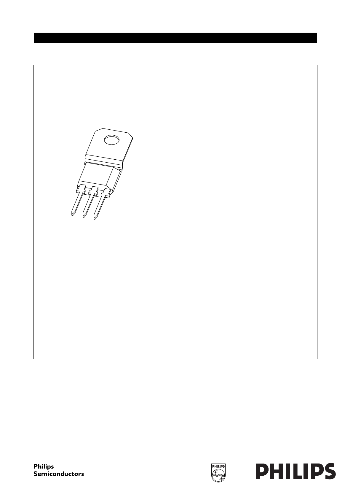
DESCRIPTION
NPN video transistor in a SOT128B
(TO-202) plastic package.
PNP complement: BFQ255A.
PINNING
PIN DESCRIPTION
page
1 emitter
APPLICATIONS
• CRT amplifier buffer/driver in
2 collector
3 base
high-resolution colour graphics
monitors.
123
MGA323
Fig.1 Simplified outline
(SOT128B; TO-202).
QUICK REFERENCE DATA
SYMBOL PARAMETER CONDITIONS MIN. TYP. MAX. UNIT
V
CBO
V
CER
I
C
P
tot
h
FE
f
T
collector-base voltage open emitter −−115 V
collector-emitter voltage RBE= 100 Ω−−110 V
collector current (DC) −−300 mA
total power dissipation Ts≤ 100 °C; note 1 −−3W
DC current gain IC= 50 mA; VCE= 10 V; T
transition frequency IC= 50 mA; VCE= 10 V; T
=25°C20 35 −
amb
=25°C 0.8 1.2 − GHz
amb
Note
is the temperature at the soldering point of the collector pin.
1. T
s
LIMITING VALUES
In accordance with the Absolute Maximum Rating System (IEC 134).
SYMBOL PARAMETER CONDITIONS MIN. MAX. UNIT
V
CBO
V
CEO
V
CER
V
EBO
I
C
P
tot
T
stg
T
j
collector-base voltage open emitter − 115 V
collector-emitter voltage open base − 95 V
collector-emitter voltage RBE= 100 Ω−110 V
emitter-base voltage open collector − 3V
collector current (DC) − 300 mA
total power dissipation Ts≤ 100 °C; note 1; see Fig.3 − 3W
storage temperature −65 +150 °C
junction temperature − 175 °C
Note
is the temperature at the soldering point of the collector pin.
1. T
s
1998 Oct 06 2

Discrete Semiconductors Product specification
NPN video transistor BFQ235A
THERMAL CHARACTERISTICS
SYMBOL PARAMETER CONDITIONS VALUE UNIT
R
th j-s
Note
1. T
s
CHARACTERISTICS
=25°C unless otherwise specified.
T
j
SYMBOL PARAMETER CONDITIONS MIN. TYP. MAX. UNIT
V
(BR)CBO
V
(BR)CEO
V
(BR)CER
V
(BR)EBO
I
CES
I
CBO
h
FE
f
T
C
cb
thermal resistance from junction to soldering point Ts≤ 100 °C; note 1 25 K/W
is the temperature at the soldering point of the collector pin.
collector-base breakdown voltage IC= 0.1 mA; IE=0 115 −−V
collector-emitter breakdown voltage IC= 10 mA; IB=0 95 −−V
collector-emitter breakdown voltage IC= 10 mA; RBE= 100 Ω 110 −−V
emitter-base breakdown voltage IE= 0.1 mA; IC=0 3 −−V
collector cut-off current IB= 0; VCE=50V −−100 µA
collector cut-off current IE= 0; VCB=50V −−20 µA
DC current gain IC= 50 mA; VCE=10V; T
amb
=25°C;
20 35 −
see Fig.4
transition frequency IC= 50 mA; VCE= 10 V; f = 100 MHz;
T
=25°C; see Fig.6
amb
collector-base capacitance IC= 0; VCB= 10 V; f = 1 MHz;
T
=25°C; see Fig.5
amb
0.8 1.2 − GHz
− 2 − pF
V
CEO
MBB887
80
(V)
400
handbook, halfpage
I
C
(mA)
300
200
100
0
0
20 40 60
Fig.2 DC SOAR.
1998 Oct 06 3
handbook, halfpage
4
P
tot
(W)
3
2
1
0
0 50 100 200
MBB888
150
Ts (oC)
Fig.3 Power derating curve.
 Loading...