

Philips BFQ162 Datasheet

DISCRETE SEMICONDUCTORS
DATA SH EET
BFQ162
NPN video transistor
Product specification
Supersedes data of November 1995
File under Discrete Semiconductors, SC05
1997 Oct 02
Philips Semiconductors Product specification
NPN video transistor BFQ162
FEATURES
• Low output capacitance
• Good thermal stability
DESCRIPTION
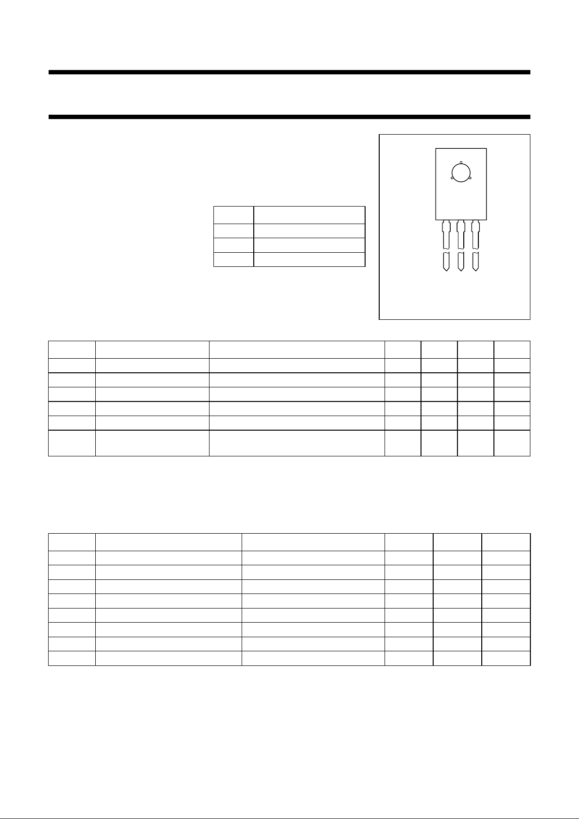
NPN video transistor in a SOT32
(TO-126) package.
alfpage
• Gold metallization ensures
excellent reliability.
PINNING
PIN DESCRIPTION
APPLICATIONS
• Pre-stage driver in high-resolution
colour graphics monitors.
1 emitter
2 collector
3 base
Top view
123
MBC077 - 1
Fig.1 Simplified outline
(SOT32; TO-126).
QUICK REFERENCE DATA
SYMBOL PARAMETER CONDITIONS MIN. TYP. MAX. UNIT
V
CBO
V
CER
I
C
P
tot
h
FE
f
T
collector-base voltage open emitter −−20 V
collector-emitter voltage RBE= 100 Ω−−19 V
collector current (DC) −−500 mA
total power dissipation Ts≤ 115 °C; note 1 −−3W
DC current gain IC= 300 mA; VCE=5V; T
transition frequency IC= 300 mA; VCE= 5 V; f = 100 MHz;
T
=25°C
amb
=25°C50 60 −
amb
1 −−GHz
Note
is the temperature at the soldering point of the collector pin.
1. T
s
LIMITING VALUES
In accordance with the Absolute Maximum Rating System (IEC 134).
SYMBOL PARAMETER CONDITIONS MIN. MAX. UNIT
V
CBO
V
CEO
V
CER
V
EBO
I
C
P
tot
T
stg
T
j
collector-base voltage open emitter − 20 V
collector-emitter voltage open base − 10 V
collector-emitter voltage RBE= 100 Ω−19 V
emitter-base voltage open collector − 3V
collector current (DC) − 500 mA
total power dissipation Ts≤ 115 °C; note 1; see Fig.3 − 3W
storage temperature −65 +175 °C
junction temperature − 175 °C
Note
is the temperature at the soldering point of the collector pin.
1. T
s
1997 Oct 02 2

Philips Semiconductors Product specification
NPN video transistor BFQ162
THERMAL CHARACTERISTICS
SYMBOL PARAMETER CONDITIONS VALUE UNIT
R
th j-s
Note
1. T
s
CHARACTERISTICS
=25°C unless otherwise specified.
T
j
SYMBOL PARAMETER CONDITIONS MIN. TYP. MAX. UNIT
V
(BR)CBO
V
(BR)CEO
V
(BR)CER
V
(BR)EBO
I
CES
h
FE
f
T
C
cb
C
c
thermal resistance from junction to soldering point Ts≤ 115 °C; note 1 20 K/W
is the temperature at the soldering point of the collector pin.
collector-base breakdown voltage IC= 5 mA; IE=0 20 −−V
collector-emitter breakdown voltage IC= 10 mA; IB=0 10 −−V
collector-emitter breakdown voltage IC= 10 mA; RBE= 100 Ω 19 −−V
emitter-base breakdown voltage IE= 1 mA; IC=0 3 −−V
collector-emitter cut-off current VBE=0V; VCE=10V −−100 µA
DC current gain IC= 300 mA; VCE=5V;
T
=25°C; see Fig.4
amb
I
= 100 mA; VCE=5V;
C
T
=25°C; see Fig.4
amb
transition frequency IC= 300 mA; VCE=5V;
f = 100 MHz; T
amb
=25°C;
50 60 −
40 50 −
1 −−GHz
see Fig.6
collector-base capacitance IC=ic= 0; VCB= 5 V; f = 1 MHz;
T
=25°C; see Fig.5
amb
− 4.2 − pF
collector capacitance IE=ie= 0; VCB= 5 V; f = 1 MHz − 5.8 − pF
1997 Oct 02 3
 Loading...