

Philips BFQ151 Datasheet

DISCRETE SEMICONDUCTORS
DATA SH EET
BFQ151
PNP video transistor
Product specification
File under Discrete Semiconductors, SC05
1997 Sep 19
Philips Semiconductors Product specification
PNP video transistor BFQ151
FEATURES
• High gain bandwidth
• Good thermal stability
• Gold metallization ensures
excellent reliability.
APPLICATIONS
• Pre-stage driver between video
amplifier and video module.
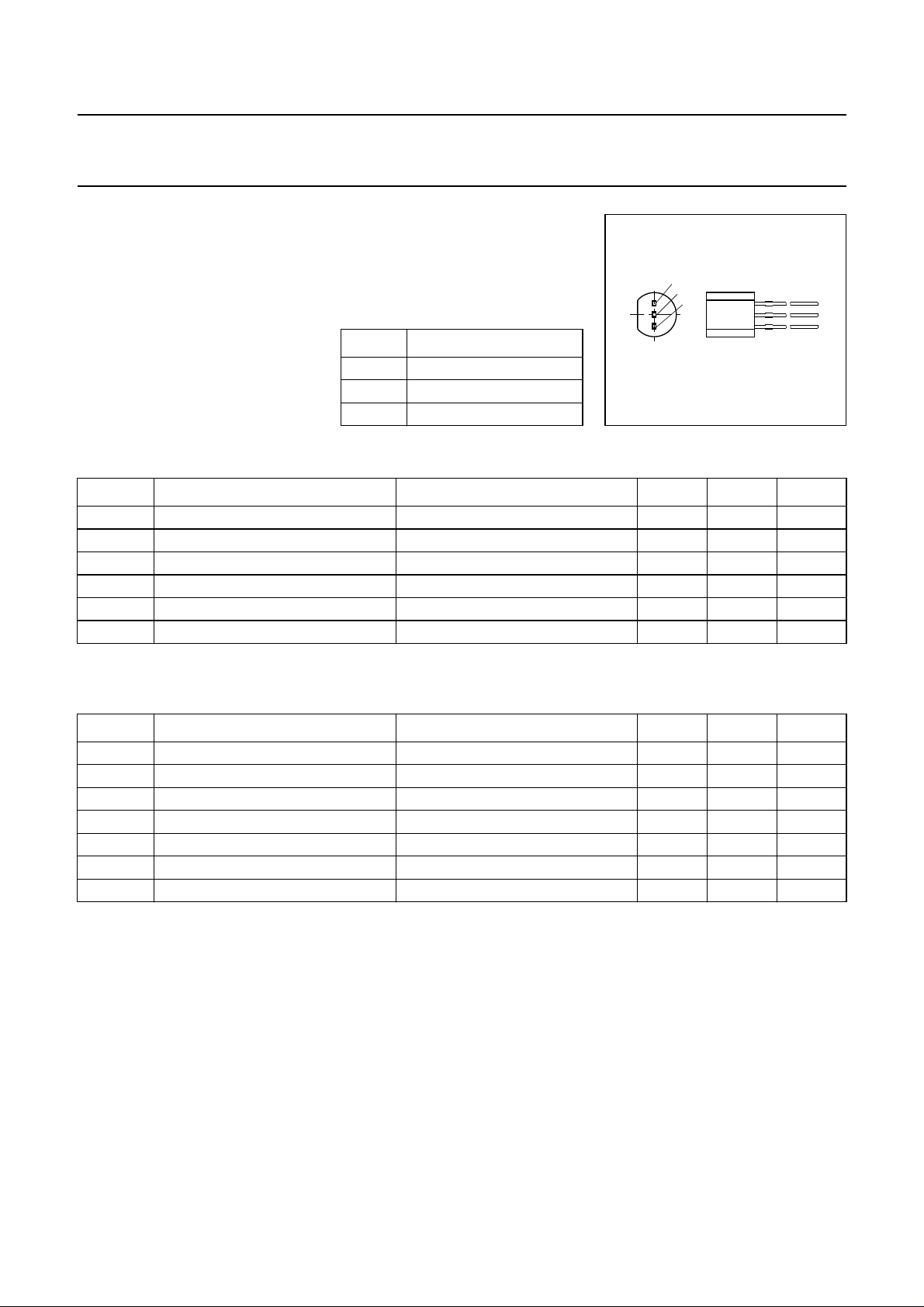
DESCRIPTION
PNP video transistor in a SOT54
plastic package.
PINNING
PIN DESCRIPTION
1 base
2 collector
3 emitter
age
1
2
3
Fig.1 Simplified outline SOT54.
MSB033
QUICK REFERENCE DATA
SYMBOL PARAMETER CONDITIONS TYP. MAX. UNIT
V
I
P
f
C
T
CBO
C
tot
T
re
j
collector-base voltage open emitter −−20 V
collector current (DC) −−100 mA
total power dissipation Ts≤ 60 °C − 1.25 W
transition frequency IC= −70 mA; VCE= −10 V 3.5 − GHz
feedback capacitance IC= 0; VCB= −10 V 1.8 − pF
junction temperature − 175 °C
LIMITING VALUES
In accordance with the Absolute Maximum Rating System (IEC 134).
SYMBOL PARAMETER CONDITIONS MIN. MAX. UNIT
V
CBO
V
CEO
V
EBO
I
C
P
tot
T
stg
T
j
collector-base voltage open emitter −−20 V
collector-emitter voltage open base −−15 V
emitter-base voltage open collector −−3V
collector current (DC) −−100 mA
total power dissipation Ts≤ 60 °C; note 1; see Fig.2 − 1.25 W
storage temperature −65 +150 °C
junction temperature − 175 °C
Note
is the temperature at the soldering point of the collector pin.
1. T
s
1997 Sep 19 2
Philips Semiconductors Product specification
PNP video transistor BFQ151
THERMAL CHARACTERISTICS
SYMBOL PARAMETER CONDITIONS VALUE UNIT
R
th j-s
Note
1. T
s
CHARACTERISTICS
=25°C unless otherwise specified.
T
j
SYMBOL PARAMETER CONDITIONS MIN. TYP. MAX. UNIT
V
(BR)CBO
V
(BR)CEO
V
(BR)EBO
I
CBO
h
FE
f
T
C
re
thermal resistance from junction to soldering point Ts≤ 60 °C; note 1 90 K/W
is the temperature of the soldering point of the collector pin.
collector-base breakdown voltage IC= −0.1 mA; IE=0 −20 −−V
collector-emitter breakdown voltage IC= −10 mA; IB=0 −15 −−V
emitter-base breakdown voltage IC= 0; IE= −0.1 mA −3 −−V
collector-base leakage current VCB= −10 V; IE=0 −−−1µA
DC current gain IC= −70 mA; VCE= −10 V;
25 −−
see Fig.3
transition frequency IC= −70 mA; VCE= −10 V;
fm= 500 MHz; T
amb
=25°C;
− 3.5 − GHz
see Fig.5
feedback capacitance IC= 0; VCB= −10 V;
− 1.8 − pF
f = 1 MHz; see Fig.4
1.6
handbook, halfpage
P
tot
(W)
1.2
0.8
0.4
0
0
100 200
Ts (
o
C)
Fig.2 Power derating curve.
MBK241
80
handbook, halfpage
h
FE
60
40
20
0
0 −20 −100
VCE= −10V; T
Fig.3 DC current gain as a function of
amb
−40 −60 −80
=25°C.
IC (mA)
collector current; typical values.
MBK242
1997 Sep 19 3
 Loading...