

Philips BFM505 Datasheet

DISCRETE SEMICONDUCTORS
DATA SH EET
BFM505
Dual NPN wideband transistor
Product specification
Supersedes data of 1995 Sep 04
File under Discrete Semiconductors, SC14
1996 Oct 08
Philips Semiconductors Product specification
Dual NPN wideband transistor BFM505
FEATURES
• Small size
• Temperature and hFE matched
• Low noise and high gain
• High gain at low current and low capacitance at low
voltage
• Gold metallization ensures excellent reliability.
APPLICATIONS
• Oscillator and buffer amplifiers
• Balanced amplifiers
• LNA/mixer.
DESCRIPTION
Dual transistor with two silicon NPN RF dies in a surface
mount, 6-pin SOT363 (S-mini) package. The transistors
are primarily intended for wideband applications in the
GHz-range in the RF front end of analog and digital cellular
phones, cordless phones, radar detectors, pagers and
satellite TV-tuners.
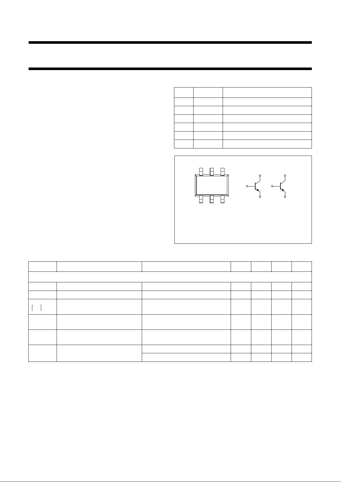
PINNING - SOT363A
PIN SYMBOL DESCRIPTION
1b
2e
3c
4b
5e
6c
64
handbook, halfpage
1
Top view
Marking code: N0.
1
1
2
2
2
1
5
2
3
base 1
emitter 1
collector 2
base 2
emitter 2
collector 1
b
1
c
1
b
2
e
1
Fig.1 Simplified outline and symbol.
c
e
MAM210
2
2
QUICK REFERENCE DATA
SYMBOL PARAMETER CONDITIONS MIN. TYP. MAX. UNIT
Any single transistor
C
re
f
T
s
21
G
UM
F noise figure I
R
th j-s
feedback capacitance Ie= 0; VCB= 3 V; f = 1 MHz − 0.22 − pF
transition frequency IC= 5 mA; VCE= 3V; f = 1 GHz − 9 − GHz
insertion power gain I
2
= 5 mA; VCE= 3 V; f = 900 MHz;
C
T
=25°C
amb
maximum unilateral power gain IC= 5 mA; VCE= 3 V; f = 900 MHz;
T
=25°C
amb
= 1 mA; VCE= 3 V; f = 900 MHz;
C
ΓS= Γ
opt
thermal resistance from junction
to soldering point
single loaded −−230 K/W
double loaded −−115 K/W
14 15 − dB
− 17 − dB
− 1.1 1.6 dB
1996 Oct 08 2
Philips Semiconductors Product specification
Dual NPN wideband transistor BFM505
LIMITING VALUES
In accordance with the Absolute Maximum System IEC 134.
SYMBOL PARAMETER CONDITIONS MIN. MAX. UNIT
Any single transistor
V
CBO
V
CEO
V
EBO
I
C
P
tot
T
stg
T
j
THERMAL CHARACTERISTICS
SYMBOL PARAMETER CONDITIONS VALUE UNIT
R
th j-s
collector-base voltage open emitter − 20 V
collector-emitter voltage open base − 8V
emitter-base voltage open collector − 2.5 V
DC collector current − 18 mA
total power dissipation up to Ts=118°C; note 1 − 500 mW
storage temperature −65 +175 °C
junction temperature − 175 °C
thermal resistance from junction
to soldering point; note 1
single loaded 230 K/W
double loaded 115 K/W
Note to the Limiting values and Thermal characteristics
1. T
is the temperature at the soldering point of the collector pin.
s
1996 Oct 08 3
 Loading...