

Philips BFG94 Datasheet

DISCRETE SEMICONDUCTORS
DATA SH EET
BFG94
NPN 6 GHz wideband transistor
Product specification
File under Discrete Semiconductors, SC14
September 1995
Philips Semiconductors Product specification
NPN 6 GHz wideband transistor BFG94
FEATURES
• High power gain
• Low noise figure
• Low intermodulation distortion
• Gold metallization ensures
excellent reliability.
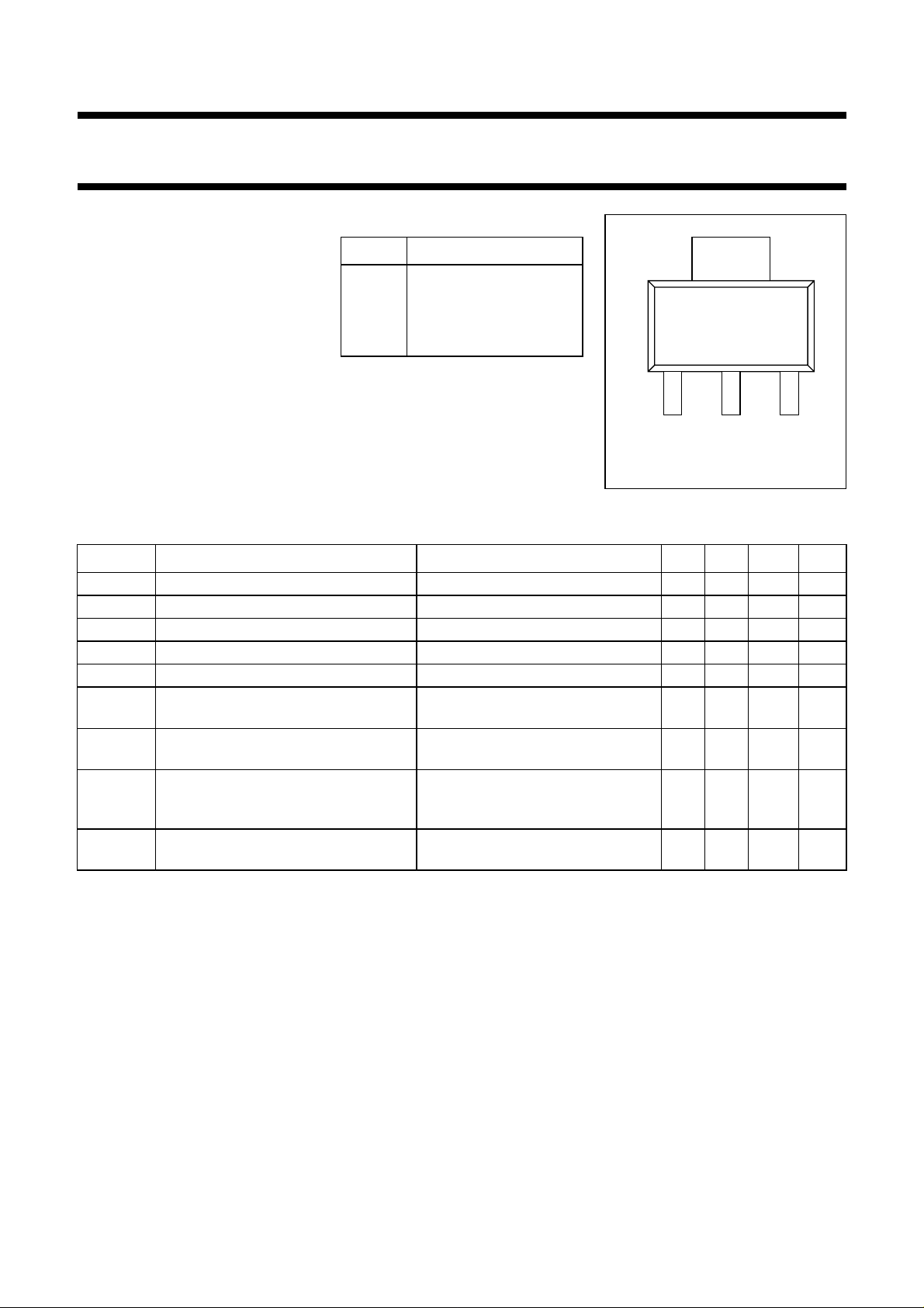
PINNING
PIN DESCRIPTION
1 emitter
2 base
3 emitter
4 collector
age
4
DESCRIPTION
NPN transistor mounted in a plastic
SOT223 envelope. It is primarily
123
Top view
MSB002 - 1
intended for use in communication
and instrumentation systems.
Fig.1 SOT223.
QUICK REFERENCE DATA
SYMBOL PARAMETER CONDITIONS MIN. TYP. MAX. UNIT
V
V
I
P
C
f
G
V
CBO
CEO
C
tot
re
T
UM
O
collector-base voltage open emitter −−15 V
collector-emitter voltage open base −−12 V
DC collector current −−60 mA
total power dissipation up to Ts = 140 °C (note 1) −−700 mW
feedback capacitance IC = 0; VCE = 10 V; f = 1 MHz −−0.8 pF
transition frequency IC = 45 mA; VCE = 10 V; f = 1 GHz;
T
= 25 °C
amb
maximum unilateral power gain IC = 45 mA; VCE = 10 V; f = 1 GHz;
T
= 25 °C
amb
output voltage IC = 45 mA; VCE = 10 V;
46− GHz
11.5 13.5 − dB
− 500 − mV
dim = −60 dB; RL = 75 Ω;
f = 800 MHz; T
P
L1
output power at 1 dB gain
compression
IC = 45 mA; VCE = 10 V; f = 1 GHz;
T
= 25 °C
amb
= 25 °C
amb
− 21.5 − dBm
Note
1. T
is the temperature at the soldering point of the collector tab.
s
September 1995 2

Philips Semiconductors Product specification
NPN 6 GHz wideband transistor BFG94
LIMITING VALUES
In accordance with the Absolute Maximum System (IEC 134).
SYMBOL PARAMETER CONDITIONS MIN. MAX. UNIT
V
CBO
V
CEO
V
EBO
I
C
P
tot
T
stg
T
j
THERMAL RESISTANCE
SYMBOL PARAMETER CONDITIONS THERMAL RESISTANCE
R
th j-s
collector-base voltage open emitter − 15 V
collector-emitter voltage open base − 12 V
emitter-base voltage open collector − 2V
DC collector current − 60 mA
total power dissipation up to Ts = 140 °C (note 1) − 700 mW
storage temperature −65 150 °C
junction temperature − 175 °C
thermal resistance from junction to
up to Ts = 140 °C (note 1) 50 K/W
soldering point
Note
1. T
is the temperature at the soldering point of the collector tab.
s
September 1995 3

Philips Semiconductors Product specification
NPN 6 GHz wideband transistor BFG94
CHARACTERISTICS
T
= 25 °C unless otherwise specified.
j
SYMBOL PARAMETER CONDITIONS MIN. TYP. MAX. UNIT
I
CBO
h
FE
C
c
C
e
C
re
f
T
G
UM
F minimum noise figure Γ
V
O
d
2
P
L1
ITO third order intercept point note 4 − 34 − dBm
collector cut-off current IE = 0; VCB = 10 V −−100 nA
DC current gain IC = 30 mA; VCE = 5 V 45 90 −
I
= 45 mA; VCE = 10 V − 100 −
C
collector capacitance IE = ie = 0; VCB = 10 V; f = 1 MHz − 0.9 2 pF
emitter capacitance IC = ie = 0; VEB = 0.5 V; f = 1 MHz − 2.9 4.5 pF
feedback capacitance IC = ic = 0; VCE = 10 V; f = 1 MHz − 0.5 0.8 pF
transition frequency IC = 45 mA; VCE = 10 V; f = 1 GHz;
T
= 25 °C
amb
I
= 30 mA; VCE = 5 V; f = 1 GHz;
C
T
= 25 °C
amb
maximum unilateral power gain
(note1)
IC = 45 mA; VCE = 10 V; f = 1 GHz;
T
= 25 °C
amb
= Γ
; IC = 45 mA; VCE = 10 V;
s
opt
4 −− GHz
46− GHz
11.5 13.5 − dB
− 2.7 − dB
f = 500 MHz
= Γ
Γ
; IC = 45 mA; VCE = 10 V;
s
opt
− 3 − dB
f = 1 GHz
output voltage note 2 − 500 − mV
second order intermodulation
note 3 −−51 − dB
distortion
output power at 1 dB gain
compression
IC = 45 mA; VCE = 10 V; RL = 50 Ω;
T
= 25 °C; measured at f = 1 GHz
amb
− 21.5 − dBm
Notes
1. G
2. d
is the maximum unilateral power gain, assuming S12 is zero and
UM
2
S
G
UM
= −60 dB (DIN 45004B, par 6.3: 3-tone); IC = 45 mA; VCE = 10 V; RL = 75 Ω; T
im
--------------------------------------------------------------
10
1S
–
21
2
1S
–
11
22
dB.log=
2
Vp = VO at dim = −60 dB; fp = 795.25 MHz;
Vq = VO−6 dB; Vr = VO−6 dB;
fq = 803.25 MHz; fr = 805.25 MHz;
measured at f
3. IC = 45 mA; VCE = 10 V; RL = 75 Ω; T
= 793.25 MHz.
(p+q−r)
= 25 °C;
amb
Vq = VO = 280 mV;
fp = 250 MHz; fq = 560 MHz;
measured at f
4. IC = 45 mA; VCE = 10 V; RL = 50 Ω;T
= 810 MHz.
(p+q)
= 25 °C;
amb
fp = 1000 MHz; fq = 1001 MHz;
measured at f
(2p−q)
and f
(2q−p
).
September 1995 4
= 25 °C;
amb
 Loading...