

Philips BFG93A-X, BFG93A Datasheet
DATA SH EET
ook, halfpage
M3D071
BFG93A; BFG93A/X
NPN 6 GHz wideband transistors
Product specification
Supersedes data of 1995 Sep 25
1998 Sep 23
Philips Semiconductors Product specification
NPN 6 GHz wideband transistors BFG93A; BFG93A/X
FEATURES
• High power gain
• Low noise figure
• Gold metallization ensures
excellent reliability.
APPLICATIONS
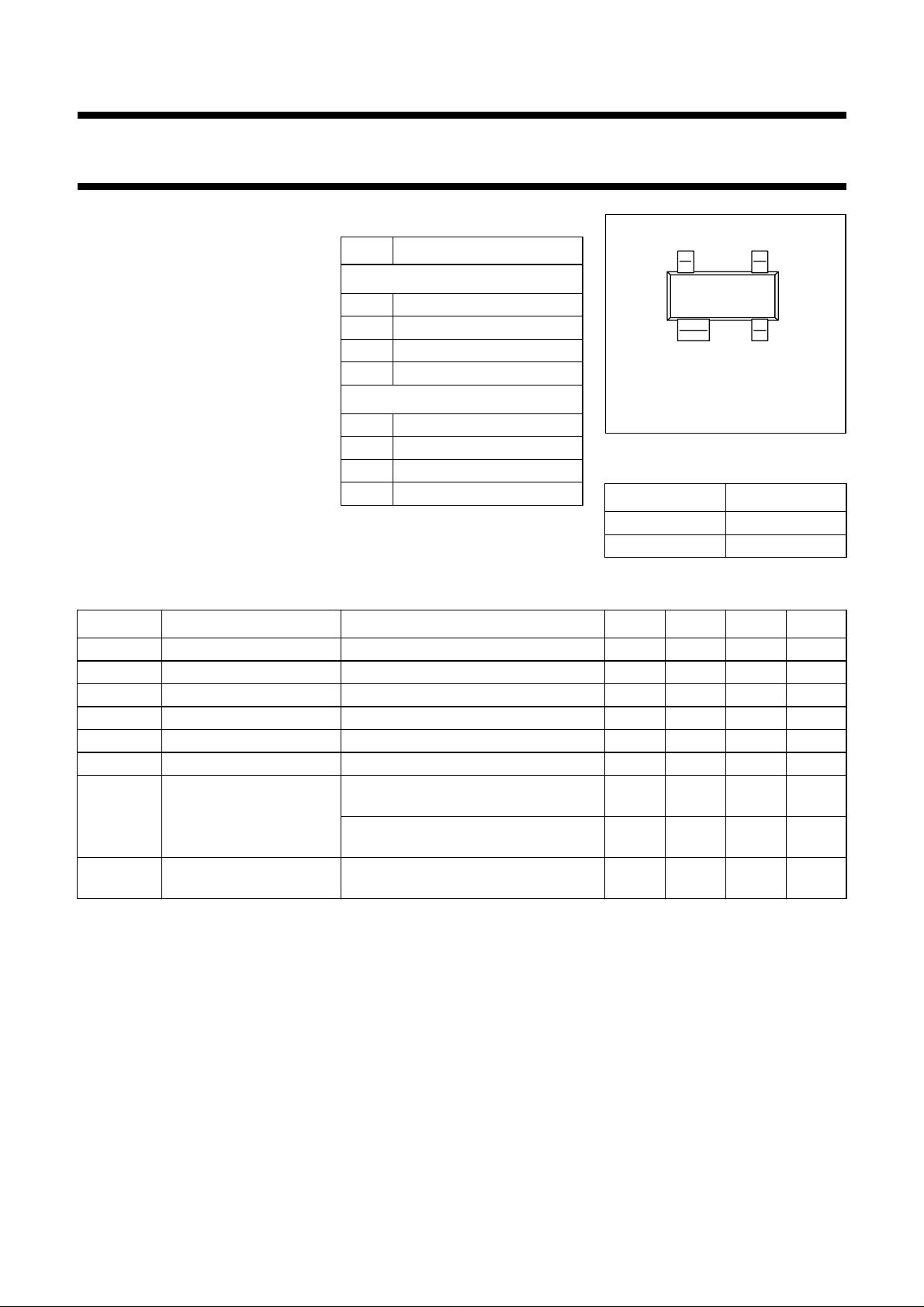
PINNING
PIN DESCRIPTION
BFG93A
1 collector
2 base
3 emitter
4 emitter
handbook, 2 columns
12
Top view
34
MSB014
Wideband applications in the UHF
and microwave range.
BFG93A/X
Fig.1 SOT143B.
1 collector
DESCRIPTION
NPN transistor in a 4-pin, dual-emitter
SOT143B plastic package.
2 emitter
3 base
4 emitter
MARKING
TYPE NUMBER CODE
BFG93A R8
BFG93A/X V15
QUICK REFERENCE DATA
SYMBOL PARAMETER CONDITIONS MIN. TYP. MAX. UNIT
V
V
I
P
C
f
G
CBO
CEO
C
tot
re
T
UM
collector-base voltage open emitter −−15 V
collector-emitter voltage open base −−12 V
collector current (DC) −−35 mA
total power dissipation Ts≤ 85 °C −−300 mW
feedback capacitance IC=ic= 0; VCB= 5 V; f = 1 MHz − 0.6 − pF
transition frequency IC= 30 mA; VCE= 5 V; f = 500 MHz 4.5 6 − GHz
maximum unilateral
power gain
IC= 30 mA; VCE=8V; T
f = 1 GHz
I
= 30 mA; VCE=8V; T
C
amb
amb
=25°C;
=25°C;
− 16 − dB
− 10 − dB
f = 2 GHz
F noise figure Γ
= Γ
; IC= 5 mA; VCE=8V;
opt
=25°C; f = 1 GHz
T
s
amb
− 1.7 − dB
1998 Sep 23 2
Philips Semiconductors Product specification
NPN 6 GHz wideband transistors BFG93A; BFG93A/X
LIMITING VALUES
In accordance with the Absolute Maximum Rating System (IEC 134).
SYMBOL PARAMETER CONDITIONS MIN. MAX. UNIT
V
CBO
V
CEO
V
EBO
I
C
P
tot
T
stg
T
j
Note
1. T
s
THERMAL CHARACTERISTICS
collector-base voltage open emitter − 15 V
collector-emitter voltage open base − 12 V
emitter-base voltage open collector − 2V
collector current (DC) − 35 mA
total power dissipation Ts≤ 85 °C; note 1 − 300 mW
storage temperature range −65 +150 °C
junction operating temperature − 175 °C
is the temperature at the soldering point of the collector pin.
SYMBOL PARAMETER CONDITIONS VALUE UNIT
R
th j-s
thermal resistance from junction to soldering point note 1 290 K/W
Note
1. T
is the temperature at the soldering point of the collector pin.
s
CHARACTERISTICS
=25°C unless otherwise specified.
T
j
SYMBOL PARAMETER CONDITIONS MIN. TYP. MAX. UNIT
I
CBO
h
C
C
C
f
T
G
FE
c
e
re
UM
collector leakage current IE= 0; VCB=5V −−50 nA
DC current gain IC= 30 mA; VCE= 5 V 40 90 −
collector capacitance IE=ie= 0; VCB=5V; f=1MHz − 0.9 − pF
emitter capacitance IC=ic= 0; VEB=5V; f=1MHz − 1.9 − pF
feedback capacitance IC=ic= 0; VCB=5V; f=1MHz − 0.6 − pF
transition frequency IC= 30 mA; VCE= 5 V; f = 500 MHz 4.5 6 − GHz
maximum unilateral power
gain; note 1
IC= 30 mA; VCE=8V; T
f = 1 GHz
I
= 30 mA; VCE=8V; T
C
amb
amb
=25°C;
=25°C;
− 16 − dB
− 10 − dB
f = 2 GHz
= Γ
F noise figure Γ
; IC= 5 mA; VCE=8V;
s
opt
T
=25°C; f = 1 GHz
amb
Γ
= Γ
; IC= 5 mA; VCE=8V;
s
opt
T
=25°C; f = 2 GHz
amb
− 1.7 − dB
− 2.3 − dB
Note
1. G
is the maximum unilateral power gain, assuming S12 is zero and
UM
1998 Sep 23 3
2
S
G
UM
10
-------------------------------------------------------------1S
–()1S
21
2
11
–()
dB.log=
2
22
Philips Semiconductors Product specification
NPN 6 GHz wideband transistors BFG93A; BFG93A/X
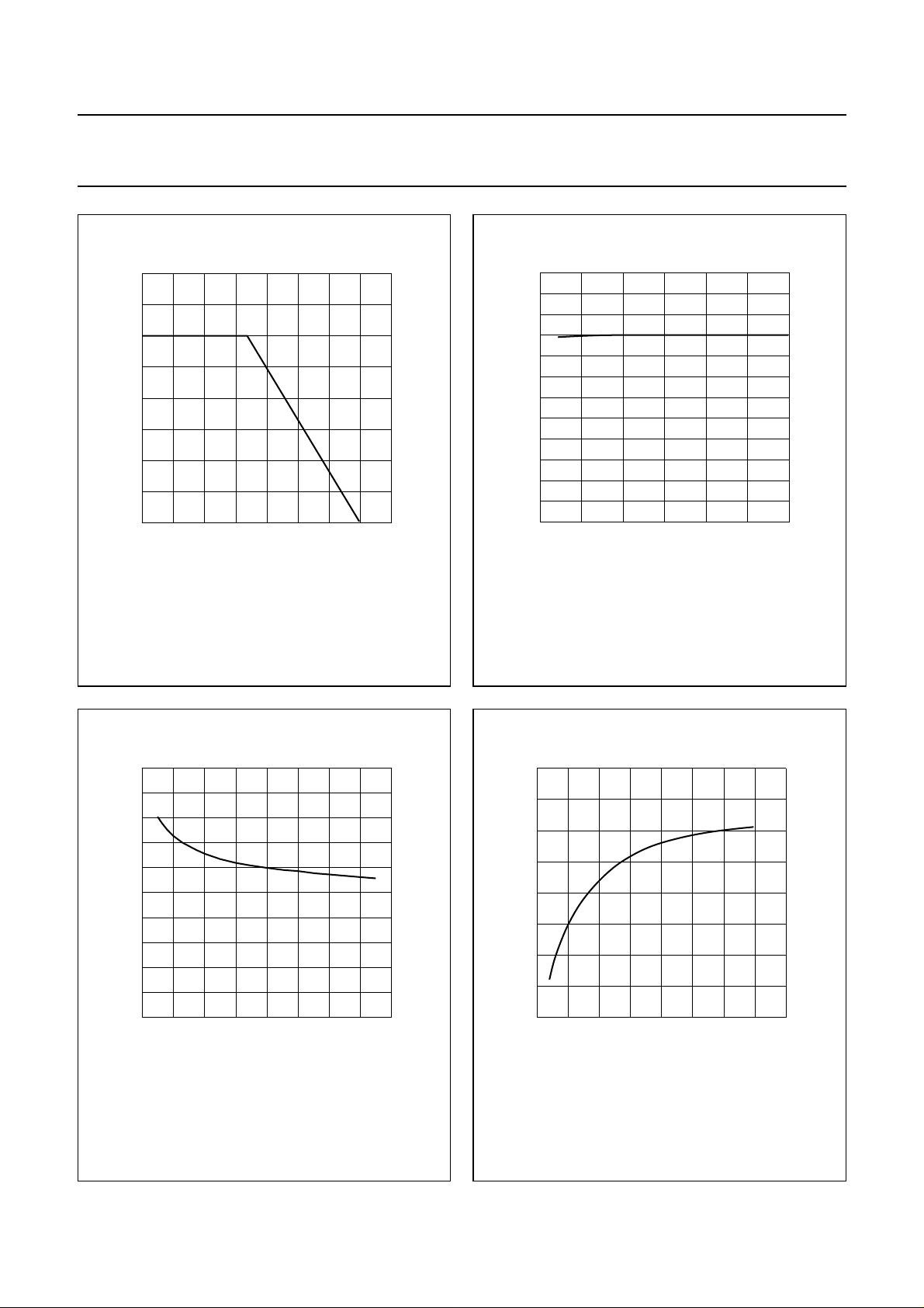
400
handbook, halfpage
P
tot
(mW)
300
200
100
0
0 50 100 200
150
Fig.2 Power derating curve.
Ts(
MBG245
o
C)
120
handbook, halfpage
h
FE
80
40
0
0102030
VCE=5V.
I (mA)
C
Fig.3 DC current gain as a function of collector
current; typical values.
MCD087
12
MCD088
V (V)
CB
1.0
handbook, halfpage
C
re
(pF)
0.8
0.6
0.4
0.2
0
048 16
IC=ic= 0; f= 1 MHz.
Fig.4 Feedback capacitance as a function of
collector-base voltage; typical values.
1998 Sep 23 4
handbook, halfpage
8
f
T
(GHz)
6
4
2
0
01020 40
VCE= 5 V; T
=25°C; f= 500MHz.
amb
Fig.5 Transition frequency as a function of
collector current; typical values.
30
MCD089
I (mA)
C
Philips Semiconductors Product specification
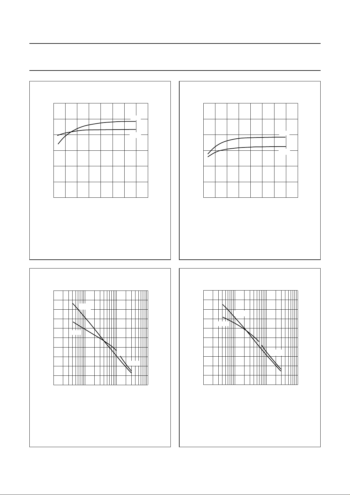
NPN 6 GHz wideband transistors BFG93A; BFG93A/X
30
handbook, halfpage
gain
(dB)
20
10
0
0
VCE= 8 V; f = 500 MHz.
10 20 40
30
MSG
G
I (mA)
C
Fig.6 Gain as a function of collector current;
typical values.
MCD090
UM
30
handbook, halfpage
gain
(dB)
30
MSG
G
I (mA)
C
20
10
0
0
VCE= 8 V; f = 1 GHz.
10 20 40
Fig.7 Gain as a function of collector current;
typical values.
MCD091
UM
50
handbook, halfpage
gain
(dB)
40
30
20
10
0
10
VCE= 8 V; IC= 10 mA.
MSG
G
UM
2
10
10
MCD092
G
max
3
f
(MHz)
4
10
Fig.8 Gain as a function of frequency; typical
values.
1998 Sep 23 5
50
handbook, halfpage
gain
(dB)
40
30
20
10
0
10
VCE= 8 V; IC=30mA.
MSG
G
UM
G
max
2
10
3
10
f (MHz)
Fig.9 Gain as a function of frequency; typical
values.
MCD093
4
10
 Loading...