

Philips BFG67W-XR, BFG67W-X, BFG67W Datasheet

DISCRETE SEMICONDUCTORS
DATA SH EET
BFG67W
BFG67W/X; BFG67W/XR
NPN 8 GHz wideband transistor
Product specification
File under Discrete Semiconductors, SC14
Philips Semiconductors
August 1995
Philips Semiconductors Product specification
NPN 8 GHz wideband transistor
FEATURES
• High power gain
• Low noise figure
• Gold metallization ensures
excellent reliability.
APPLICATIONS
They are intended for wideband
applications in the GHz range such as
analog satellite television systems
and portable RF communication
equipment.
DESCRIPTION
NPN silicon planar epitaxial
transistors in plastic, 4-pin
dual-emitter SOT343 and SOT343R
packages.
MARKING
TYPE NUMBER CODE
BFG67W V2
BFG67W/X V6
BFG67W/XR V7
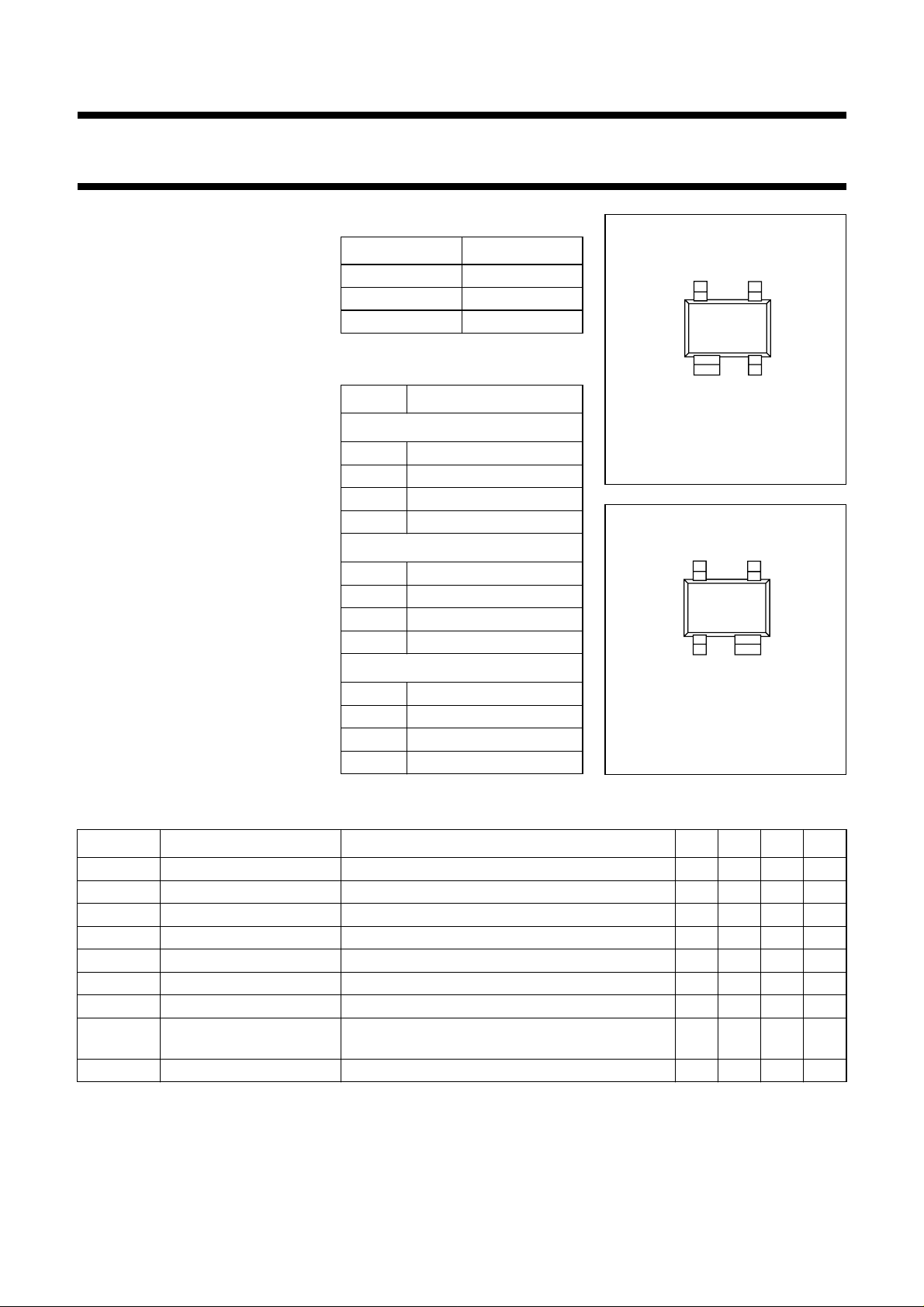
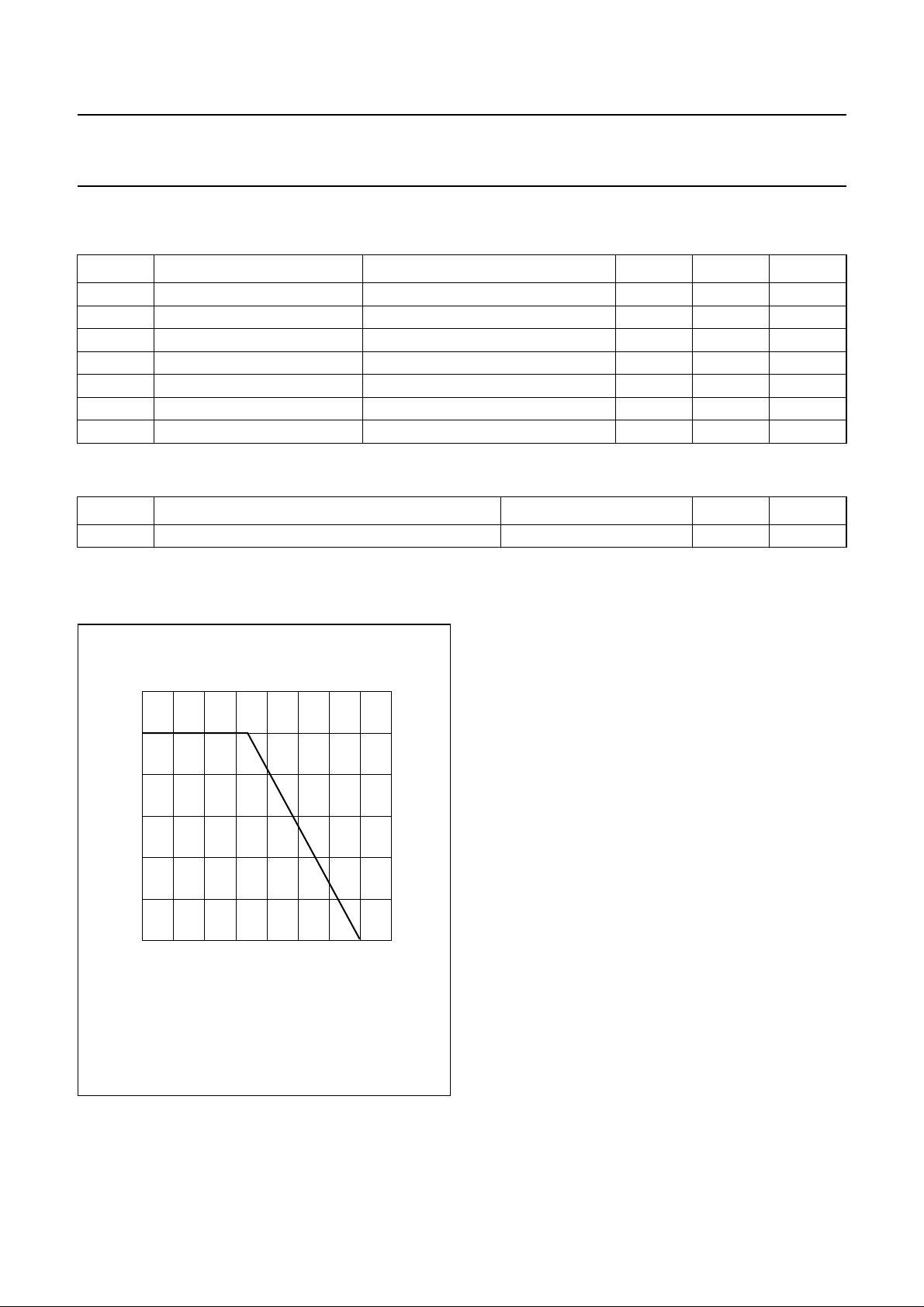
PINNING
PIN DESCRIPTION
BFG67W (see Fig.1)
1 collector
2 base
3 emitter
4 emitter
BFG67W/X (see Fig.1)
1 collector
2 emitter
3 base
4 emitter
BFG67W/XR (see Fig.2)
1 collector
2 emitter
3 base
4 emitter
BFG67W
BFG67W/X; BFG67W/XR
page
Top view
Fig.1 SOT343.
lfpage
21
Top view
Fig.2 SOT343R.
34
21
MBK523
43
MSB842
QUICK REFERENCE DATA
SYMBOL PARAMETER CONDITIONS MIN. TYP. MAX. UNIT
V
V
I
P
h
C
f
G
CBO
CEO
C
tot
FE
re
T
UM
collector-base voltage open emitter −−20 V
collector-emitter voltage open base −−10 V
collector current (DC) −−50 mA
total power dissipation up to Ts=85°C −−500 mW
DC current gain IC= 15 mA; VCE= 5 V 60 100 −
feedback capacitance IC= 0; VCE= 8 V; f = 1 MHz − 0.5 − pF
transition frequency IC= 15 mA; VCE= 8 V; f = 500 MHz; T
maximum unilateral
IC= 15 mA; VCE= 8 V; f = 1 GHz; T
=25°C − 7.5 − GHz
amb
=25°C − 15.5 − dB
amb
power gain
F noise figure Γ
; IC= 5 mA; VCE= 8 V; f = 2 GHz − 2.2 − dB
s=Γopt
August 1995 2
Philips Semiconductors Product specification
NPN 8 GHz wideband transistor
BFG67W
BFG67W/X; BFG67W/XR
LIMITING VALUES
In accordance with the Absolute Maximum Rating System (IEC 134).
SYMBOL PARAMETER CONDITIONS MIN. MAX. UNIT
V
CBO
V
CEO
V
EBO
I
C
P
tot
T
stg
T
j
THERMAL CHARACTERISTICS
SYMBOL PARAMETER CONDITIONS VALUE UNIT
R
th j-s
Note to the “Limiting values” and “Thermal characteristics”
1. T
s
collector-base voltage open emitter − 20 V
collector-emitter voltage open base − 10 V
emitter-base voltage open collector − 2.5 V
collector current (DC) − 50 mA
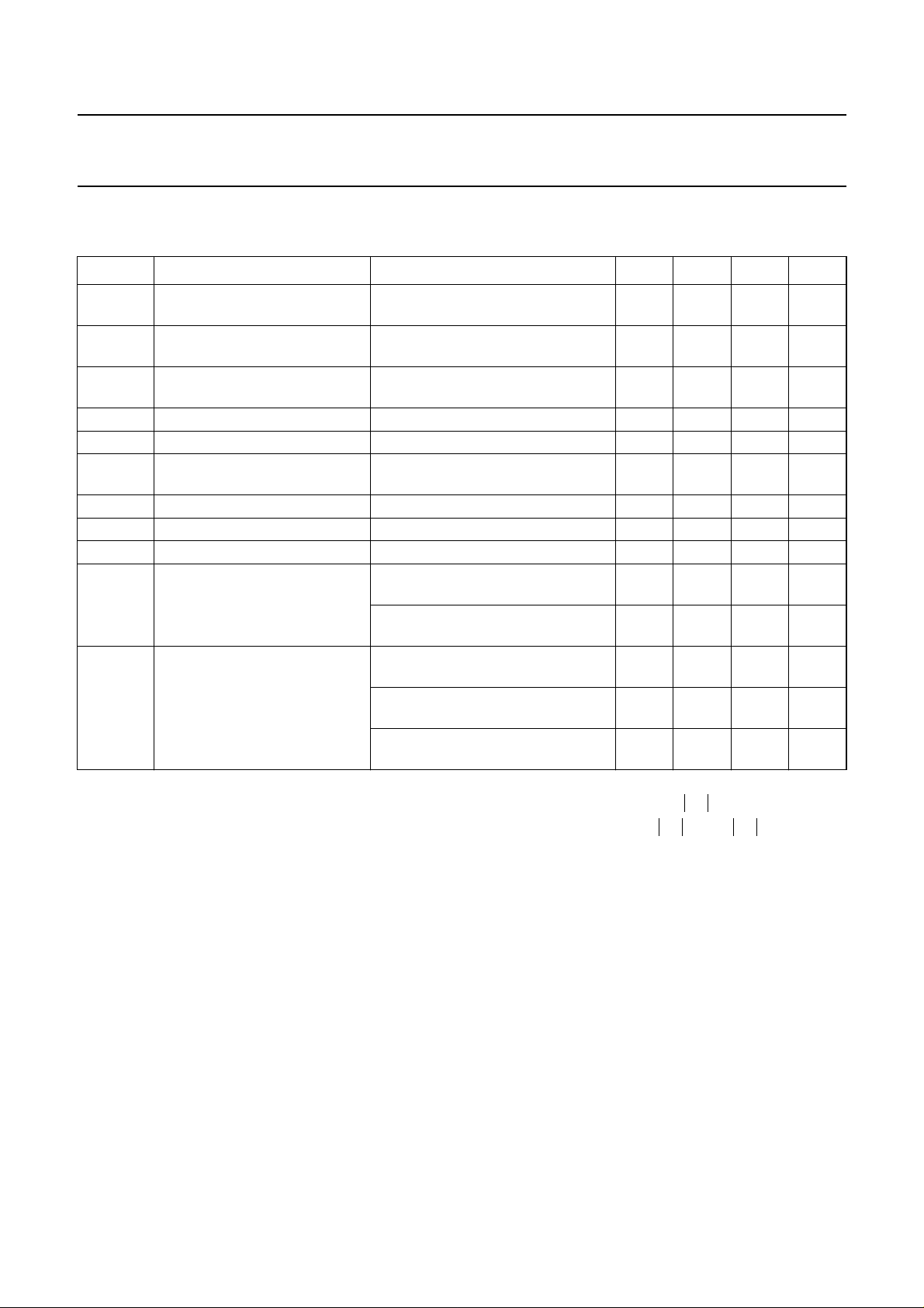
total power dissipation up to Ts=85°C; see Fig.3; note 1 − 500 mW
storage temperature −65 +150 °C
junction temperature − 175 °C
thermal resistance from junction to soldering point up to Ts=85°C; note 1 180 K/W
is the temperature at the soldering point of the collector pin.
600
handbook, halfpage
P
tot
(mW)
400
200
0
0 50 100 200
150
T ( C)
Fig.3 Power derating curve.
MBG248
s
o
August 1995 3
Philips Semiconductors Product specification
NPN 8 GHz wideband transistor
BFG67W
BFG67W/X; BFG67W/XR
CHARACTERISTICS
T
=25°C (unless otherwise specified).
j
SYMBOL PARAMETER CONDITIONS MIN. TYP. MAX. UNIT
V
(BR)CBO
collector-base breakdown
voltage
V
(BR)CEO
collector-emitter breakdown
voltage
V
(BR)EBO
emitter-base breakdown
voltage
I
CBO
h
f
T
C
C
C
G
FE
c
e
re
UM
collector cut-off current open emitter; VCB= 5 V; IE=0 −−50 nA
DC current gain IC= 15 mA; VCE= 5 V 60 100 −
transition frequency IC= 15 mA; VCE= 8 V; f = 500 MHz;
collector capacitance IE=ie= 0; VCE= 8 V; f = 1 MHz − 0.7 − pF
emitter capacitance IC=ic= 0; VEB= 0.5 V; f = 1 MHz − 1.3 − pF
feedback capacitance IC= 0; VCE= 8 V; f = 1 MHz − 0.5 − pF
maximum unilateral power
gain; note 1
F noise figure Γ
open emitter; IC=10µA; IE=0 −−20 V
open base; IC= 10 mA; IB=0 −−10 V
open collector; IE=10µA; IC=0 −−2.5 V
− 7.5 − GHz
T
=25°C
amb
IC= 15 mA; VCE= 8 V; f = 1 GHz;
T
=25°C
amb
= 15 mA; VCE= 8 V; f = 2 GHz;
I
C
T
=25°C
amb
; IC= 5 mA; VCE=8V;
s=Γopt
− 15.5 − dB
− 10 − dB
− 1.3 − dB
f = 1 GHz
Γ
; IC= 15 mA; VCE=8V;
s=Γopt
− 1.7 − dB
f = 1 GHz
Γ
; IC= 5 mA; VCE=8V;
s=Γopt
− 2.2 − dB
f = 2 GHz
Note
1. G
is the maximum unilateral power gain, assuming s12 is zero.
UM
August 1995 4
2
s
G
UM
10
-----------------------------------------------------------1s
–()1s
21
2
11
–()
dB.log=
2
22

Philips Semiconductors Product specification
NPN 8 GHz wideband transistor
120
handbook, halfpage
h
FE
80
40
0
0
20 40
MBB301
I (mA)
C
BFG67W
BFG67W/X; BFG67W/XR
handbook, halfpage
60
1
C
re
(pF)
0.8
0.6
0.4
0.2
0
048 16
MLB984
12
(V)
V
CB
VCE=5V.
Fig.4 DC current gain as a function of collector
current; typical values.
30
MLB985
I (mA)
C
10
handbook, halfpage
f
T
(GHz)
8
6
4
2
0
01020 40
IC= 0; f= 1 MHz.
Fig.5 Feedbackcapacitance as a function of
collector-base voltage; typical values.
f = 2 GHz; VCE= 8 V; T
amb
=25°C.
Fig.6 Transition frequency as a function of
collector current; typical values.
August 1995 5
 Loading...