

DISCRETE SEMICONDUCTORS
DATA SH EET
BFG591
NPN 7 GHz wideband transistor
Product specification
Supersedes data of November 1992
File under Discrete Semiconductors, SC14
1995 Sep 04
Philips Semiconductors Product specification
NPN 7 GHz wideband transistor BFG591
FEATURES
• High power gain
• Low noise figure
DESCRIPTION
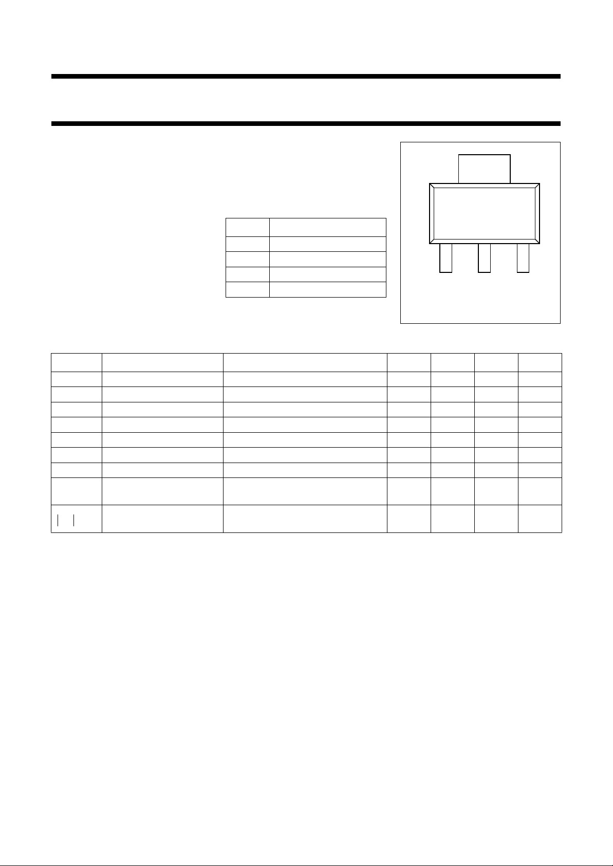
NPN silicon planar epitaxial transistor
in a plastic, 4-pin SOT223 package.
page
4
• High transition frequency
• Gold metallization ensures
excellent reliability.
PINNING
PIN DESCRIPTION
1 emitter
APPLICATIONS
Intended for applications in the GHz
range such as MATV or CATV
amplifiers and RF communications
subscriber equipment.
2 base
3 emitter
4 collector
123
Top view
MSB002 - 1
Fig.1 SOT223.
QUICK REFERENCE DATA
SYMBOL PARAMETER CONDITIONS MIN. TYP. MAX. UNIT
V
CBO
V
CEO
I
C
P
tot
h
FE
C
re
f
T
G
UM
s
21
collector-base voltage open emitter −−20 V
collector-emitter voltage open base −−15 V
collector current (DC) −−200 mA
total power dissipation up to Ts=80°C; note 1 −−2W
DC current gain IC= 70 mA; VCE= 8 V 60 90 250
feedback capacitance IC=Ic= 0; VCE= 12 V; f = 1 MHz − 0.7 − pF
transition frequency IC= 70 mA; VCE=12V; f=1GHz − 7 − GHz
maximum unilateral
power gain
insertion power gain I
2
IC= 70 mA; VCE=12V;
f = 900 MHz; T
= 70 mA; VCE=12V;
C
f = 900 MHz; T
amb
amb
=25°C
=25°C
− 13 − dB
− 12 − dB
Note
1. T
is the temperature at the soldering point of the collector pin.
s
1995 Sep 04 2

Philips Semiconductors Product specification
NPN 7 GHz wideband transistor BFG591
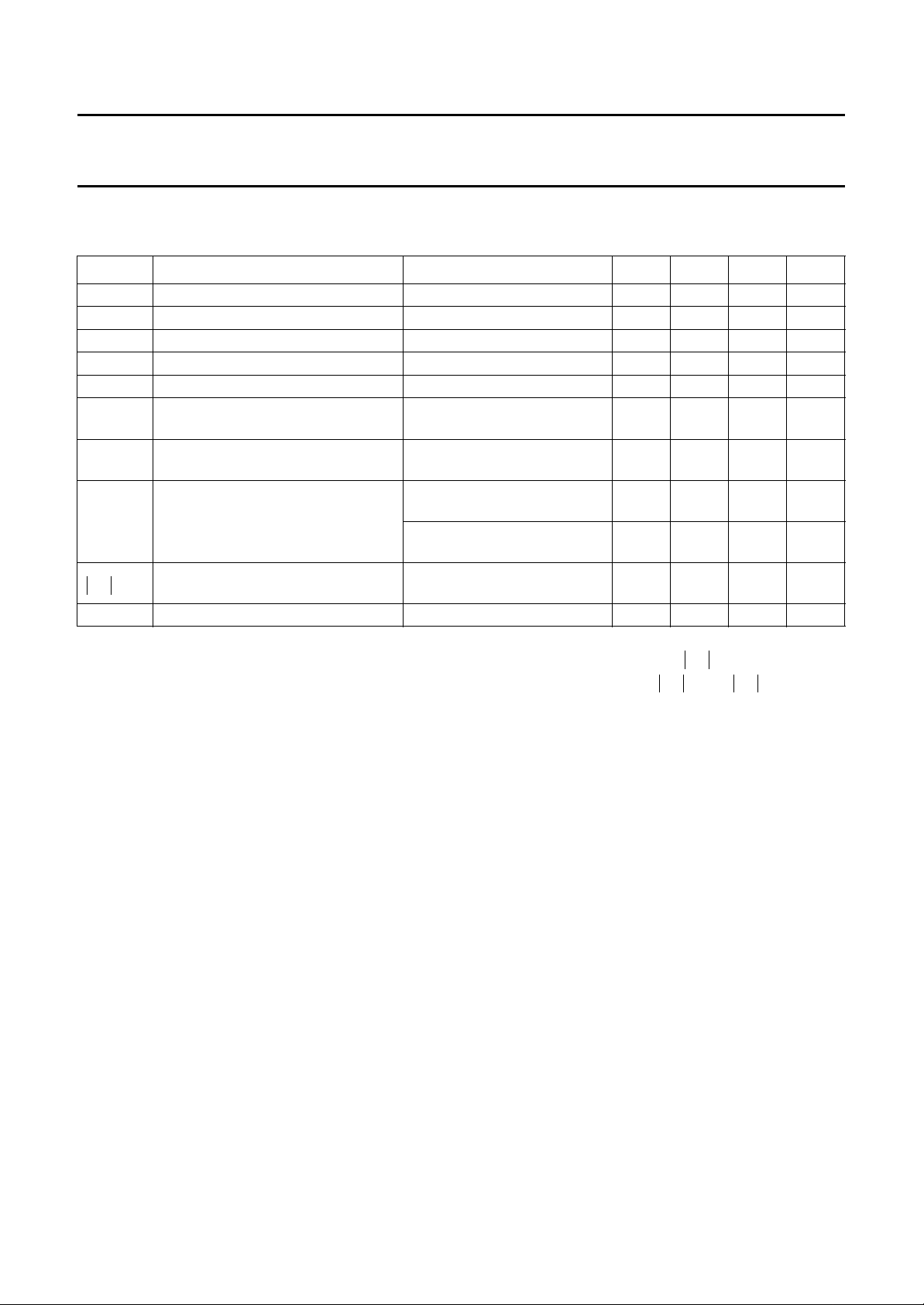
LIMITING VALUES
In accordance with the Absolute Maximum Rating System (IEC 134).
SYMBOL PARAMETER CONDITIONS MIN. MAX. UNIT
V
CBO
V
CEO
V
EBO
I
C
P
tot
T
stg
T
j
THERMAL CHARACTERISTICS
SYMBOL PARAMETER CONDITIONS VALUE UNIT
R
th j-s
collector-base voltage open emitter − 20 V
collector-emitter voltage open base − 15 V
emitter-base voltage open collector − 3V
collector current (DC) − 200 mA
total power dissipation up to Ts=80°C; note 1 − 2W
storage temperature −65 +150 °C
junction temperature − 150 °C
thermal resistance from junction to
note 1 35 K/W
soldering point
Note to the Limiting values and Thermal characteristics
1. T
is the temperature at the soldering point of the collector pin.
s
1995 Sep 04 3
Philips Semiconductors Product specification
NPN 7 GHz wideband transistor BFG591
CHARACTERISTICS
T
=25°C (unless otherwise specified).
j
SYMBOL PARAMETER CONDITIONS MIN. TYP. MAX. UNIT
V
(BR)CBO
V
(BR)CES
V
(BR)EBO
I
CBO
h
FE
C
re
f
T
G
UM
s
21
V
o
collector-base breakdown voltage IC= 0.1 mA; IE=0 −−20 V
collector-emitter breakdown voltage IC= 10 mA; IB=0 −−15 V
emitter-base breakdown voltage IE= 0.1 mA; IC=0 −−3V
collector-base leakage current IE= 0; VCB=10V −−100 nA
DC current gain IC= 70 mA; VCE=8V 6090250
feedback capacitance IB=Ib= 0; VCE=12V;
− 0.7 − pF
f = 1 MHz
transition frequency IC= 70 mA; VCE=12V;
− 7 − GHz
f = 1 GHz
maximum unilateral power gain;
note 1
insertion power gain I
2
IC= 70 mA; VCE=12V;
f = 900 MHz; T
I
= 70 mA; VCE=12V;
C
f = 2 GHz; T
= 70 mA; VCE=12V;
C
f = 1 GHz; T
amb
amb
amb
=25°C
=25°C
=25°C
− 13 − dB
− 7.5 − dB
− 12 − dB
output voltage note 2 − 700 − mV
Notes
1. G
is the maximum unilateral power gain, assuming s12 is zero.
UM
2. dim= 60 dB (DIN45004B);
Vp=Vo;Vq=Vo−6 dB; Vr=Vo−6 dB;
fp= 795.25 MHz; fq= 803.25 MHz; fr= 803.25 MHz; measured at f
G
UM
= 793.25 MHz.
(p+q-r)
10
-----------------------------------------------------------1s
–()1s
11
2
s
21
2
–()
22
dB.log=
2
1995 Sep 04 4
 Loading...