

Philips BFG505-X, BFG505 Datasheet

DISCRETE SEMICONDUCTORS
DATA SH EET
ook, halfpage
M3D071
BFG505; BFG505/X
NPN 9 GHz wideband transistors
Product specification
Supersedes data of September 1995
1998 Oct 02
Philips Semiconductors Product specification
NPN 9 GHz wideband transistors BFG505; BFG505/X
FEATURES
• High power gain
• Low noise figure
• High transition frequency
• Gold metallization ensures excellent reliability.
APPLICATIONS
RF front end applications in the GHz range, such as
analog and digital cellular telephones, cordless telephones
(CT1, CT2, DECT, etc.), radar detectors, pagers and
satellite TV tuners (SATV).
DESCRIPTION
NPN silicon planar epitaxial transistor in a 4-pin
dual-emitter SOT143B plastic package.
MARKING
TYPE NUMBER CODE
BFG505 N33
BFG505/X N39
PINNING
DESCRIPTION
PIN
BFG505 BFG505/X
1 collector collector
2 base emitter
3 emitter base
4 emitter emitter
handbook, 2 columns
12
Top view
Fig.1 Simplified outline SOT143B.
34
MSB014
QUICK REFERENCE DATA
SYMBOL PARAMETER CONDITIONS MIN. TYP. MAX. UNIT
V
CBO
V
CES
I
C
P
tot
h
FE
C
re
f
T
G
UM
2
S
21
F noise figure Γ
collector-base voltage open emitter −−20 V
collector-emitter voltage RBE=0 −−15 V
collector current (DC) −−18 mA
total power dissipation Ts≤ 130 °C −−150 mW
DC current gain VCE=6V; IC= 5 mA 60 120 250
feedback capacitance VCB=6V; IC=ic= 0; f = 1 MHz − 0.2 − pF
transition frequency VCE=6V; IC= 5 mA; f = 1 GHz − 9 − GHz
maximum unilateral
power gain
insertion power gain VCE=6V; Ic= 5 mA;
VCE=6V; IC= 5 mA;
T
=25°C; f = 900 MHz
amb
V
=6V; IC= 5 mA;
CE
T
=25°C; f = 2 GHz
amb
T
=25°C; f = 900 MHz
amb
= Γ
s
opt;VCE
T
=25°C; f = 900 MHz
amb
Γ
= Γ
s
opt;VCE
T
=25°C; f = 900 MHz
amb
Γ
= Γ
s
opt
T
=25°C; f = 2 GHz
amb
=6V; Ic= 1.25 mA;
=6V; Ic= 5 mA;
; VCE=6V; Ic= 1.25 mA;
− 20 − dB
− 13 − dB
16 17 − dB
− 1.2 1.7 dB
− 1.6 2.1 dB
− 1.9 − dB
1998 Oct 02 2
Philips Semiconductors Product specification
NPN 9 GHz wideband transistors BFG505; BFG505/X
LIMITING VALUES
In accordance with the Absolute Maximum System (IEC 134).
SYMBOL PARAMETER CONDITIONS MIN. MAX. UNIT
V
CBO
V
CES
V
EBO
I
C
P
tot
T
stg
T
j
Note
1. T
is the temperature at the soldering point of the collector pin.
s
THERMAL CHARACTERISTICS
collector-base voltage open emitter − 20 V
collector-emitter voltage RBE=0 − 15 V
emitter-base voltage open collector − 2.5 V
collector current (DC) − 18 mA
total power dissipation Ts≤ 130 °C; see Fig.2; note 1 − 150 mW
storage temperature range −65 150 °C
junction temperature − 175 °C
SYMBOL PARAMETER CONDITIONS VALUE UNIT
R
th j-s
thermal resistance from junction to soldering point note 1 290 K/W
Note
is the temperature at the soldering point of the collector pin.
1. T
s
200
handbook, halfpage
P
tot
(mW)
150
100
50
MRA638-1
0
0 50 100 200
150
Ts (°C)
Fig.2 Power derating curve.
1998 Oct 02 3

Philips Semiconductors Product specification
NPN 9 GHz wideband transistors BFG505; BFG505/X
CHARACTERISTICS
T
= 25 °C unless otherwise specified.
j
SYMBOL PARAMETER CONDITIONS MIN. TYP. MAX. UNIT
I
CBO
h
FE
C
e
C
c
C
re
f
T
G
UM
S
21
F noise figure Γ
P
L1
ITO third order intercept point note 2 − 10 − dBm
collector cut-off current VCB=6V; IE=0 −− 50 nA
DC current gain IC= 5 mA; VCE= 6 V; see Fig.3 60 120 250
emitter capacitance IC=ic=0 VEB= 0.5 V; f = 1 MHz − 0.4 − pF
collector capacitance VCB=6V; IE=ie= 0; f = 1 MHz − 0.3 − pF
feedback capacitance IC= 0; VCB= 6 V; f = 1 MHz; see Fig.4 − 0.2 − pF
transition frequency IC= 5 mA; VCE= 6 V; f = 1 GHz;
− 9 − GHz
see Fig.5
maximum unilateral
power gain; note 1
2
insertion power gain Ic= 5 mA; VCE=6V;
output power at 1 dB gain
compression
IC= 5 mA; VCE=6V;
T
=25°C; f = 900 MHz
amb
I
= 5 mA; VCE=6V;
c
T
=25°C; f = 2 GHz
amb
T
=25°C; f = 900 MHz
amb
= Γ
; IC= 1.25 mA; VCE=6V;
s
opt
T
=25°C; f = 900 MHz
amb
= Γ
Γ
T
Γ
T
; IC= 5 mA; VCE=6V;
s
opt
=25°C; f = 900 MHz
amb
= Γ
; IC= 1.25 mA; VCE=6V;
s
opt
=25°C; f = 2 GHz
amb
IC= 5 mA; VCE=6V; RL=50Ω;
T
=25°C; f = 900 MHz
amb
− 20 − dB
− 13 − dB
16 17 − dB
− 1.2 1.7 dB
− 1.6 2.1 dB
− 1.9 − dB
− 4 − dBm
Notes
1. G
2. VCE= 6 V; IC= 5 mA; RL=50Ω; T
is the maximum unilateral power gain, assuming S12is zero and
UM
=25°C;
amb
fp= 900 MHz; fq= 902 MHz;
measured at 2fp− fq= 898 MHz and 2fq− fp= 904 MHz.
1998 Oct 02 4
2
S
G
UM
--------------------------------------------------------------
10
1S
–()1S
21
2
11
–()
dB.log=
2
22
Philips Semiconductors Product specification
NPN 9 GHz wideband transistors BFG505; BFG505/X
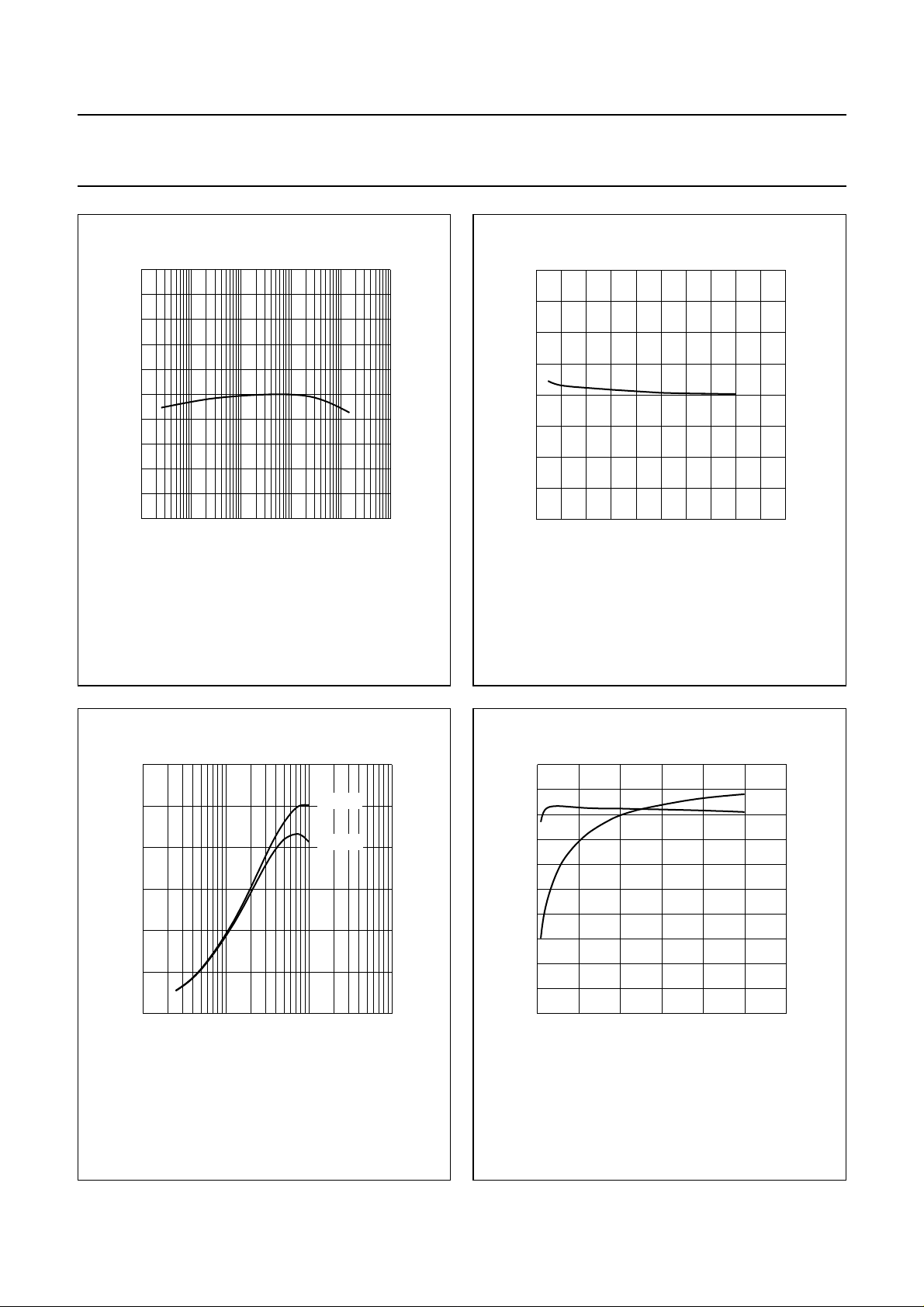
250
handbook, halfpage
h
FE
200
150
100
50
0
−3
10
VCE=6V.
−2
10
−1
10
110
MRA639
I
(mA)
C
Fig.3 DC current gain as a function of collector
current.
0.4
handbook, halfpage
C
re
(pF)
0.3
0.2
0.1
2
10
0
02 10
IC= 0; f= 1 MHz.
46 8
MRA640
VCB (V)
Fig.4 Feedback capacitance as a function of
collector-base voltage.
12
handbook, halfpage
f
T
(GHz)
8
4
0
−1
10
T
=25°C; f= 1GHz.
amb
11010
V
CE
V
CE
Fig.5 Transition frequency as a function of
collector current.
= 6 V
= 3 V
IC (mA)
MRA641
2
25
handbook, halfpage
gain
(dB)
20
15
10
5
0
04
VCE= 6 V; f = 900 MHz.
GUM= maximum unilateral power gain;
MSG = maximum stable gain;
= maximum available gain.
G
max
G
UM
MSG
812
Fig.6 Gain as a function of collector current.
MRA642
I
(mA)
C
1998 Oct 02 5
 Loading...