


DISCRETE SEMICONDUCTORS
M3D124
BFG480W
NPN wideband transistor
Product specification
Supersedes data of 1998 Jul 09
1998 Oct 21
Philips Semiconductors Product specification
NPN wideband transistor BFG480W
FEATURES
• High power gain
• High efficiency
• Low noise figure
• High transition frequency
• Emitter is thermal lead
• Low feedback capacitance
• Linear and non-linear operation.
APPLICATIONS
• RF front end with high linearity system demands
(CDMA)
• Common emitter class AB driver.
DESCRIPTION
NPN double polysilicon wideband transistor with buried
layer for low voltage applications in a 4-pin dual-emitter
SOT343R plastic package.
QUICK REFERENCE DATA
PINNING
PIN DESCRIPTION
1 emitter
2 base
3 emitter
4 collector
handbook, halfpage
Marking code: P6.
43
21
Top view
MSB842
Fig.1 Simplified outline SOT343R.
SYMBOL PARAMETER CONDITIONS TYP. MAX. UNIT
V
CEO
I
C
P
tot
f
T
G
max
F noise figure I
G
p
collector-emitter voltage open base − 4.5 V
collector current (DC) 80 250 mA
total power dissipation Ts≤ 60 °C − 360 mW
transition frequency IC= 80 mA; VCE= 2 V; f = 2 GHz; T
maximum gain IC= 80 mA; VCE= 2 V; f = 2 GHz; T
= 8 mA; VCE= 2 V; f = 2 GHz; ΓS= Γ
C
power gain Pulsed; class-AB; δ < 1 : 2; tp= 5 ms;
=25°C21 − GHz
amb
=25°C16 − dB
amb
opt
1.8 − dB
13.5 − dB
VCE= 3.6 V; f = 2 GHz; PL= 100 mW
η
C
collector efficiency Pulsed; class-AB; δ < 1 : 2; tp= 5 ms;
45 − %
VCE= 3.6 V; f = 2 GHz; PL= 100 mW
CAUTION
This product is supplied in anti-static packing to prevent damage caused by electrostatic discharge during transport
and handling. For further information, refer to Philips specs.: SNW-EQ-608, SNW-FQ-302A, and SNW-FQ-302B.
1998 Oct 21 2

Philips Semiconductors Product specification
NPN wideband transistor BFG480W
LIMITING VALUES
In accordance with the Absolute Maximum Rating System (IEC 134).
SYMBOL PARAMETER CONDITIONS MIN. MAX. UNIT
V
CBO
V
CEO
V
EBO
I
C
P
tot
T
stg
T
j
Note
1. T
s
THERMAL CHARACTERISTICS
collector-base voltage open emitter − 14.5 V
collector-emitter voltage open base − 4.5 V
emitter-base voltage open collector − 1V
collector current (DC) − 250 mA
total power dissipation Ts≤ 60 °C; note 1; see Fig.2 − 360 mW
storage temperature −65 +150 °C
operating junction temperature − 150 °C
is the temperature at the soldering point of the emitter pins.
SYMBOL PARAMETER VALUE UNIT
R
th j-s
handbook, halfpage
P
tot
(mW)
thermal resistance from junction to soldering point 250 K/W
120
MGR623
Ts (°C)
500
400
300
200
100
0
0 40 80 160
Fig.2 Power derating curve.
1998 Oct 21 3

Philips Semiconductors Product specification
NPN wideband transistor BFG480W
CHARACTERISTICS
=25°C unless otherwise specified.
T
j
SYMBOL PARAMETER CONDITIONS MIN. TYP. MAX. UNIT
V
(BR)CBO
V
(BR)CEO
V
(BR)EBO
I
CBO
h
FE
C
c
C
e
C
re
f
T
G
max
S
21
F noise figure I
P
L1
ITO third order intercept point I
collector-base breakdown voltage IC=50µA; IE= 0 14.5 −−V
collector-emitter breakdown voltage IC= 5 mA; IB= 0 4.5 −−V
emitter-base breakdown voltage IE= 100 µA; IC=0 1 −−V
collector-base leakage current VCE=5V; VBE=0 −−70 nA
DC current gain IC= 80 mA; VCE= 2 V; see Fig.3 40 60 100
collector capacitance IE=ie= 0; VCB= 2 V; f = 1 MHz − 1.4 − pF
emitter capacitance IC=ic= 0; VEB= 0.5 V; f = 1 MHz − 2.2 − pF
feedback capacitance IC= 0; VCB= 2 V; f = 1 MHz;
− 340 − fF
see Fig.4
transition frequency IC= 80 mA; VCE= 2 V; f = 2 GHz;
T
=25°C; see Fig.5
amb
maximum power gain; note 1 IC= 80 mA; VCE= 2 V; f = 2 GHz;
T
=25°C; see Figs 7 and 8
amb
insertion power gain I
2
output power at 1 dB gain
compression
= 80 mA; VCE= 2 V; f = 2 GHz;
C
T
=25°C; see Fig.8
amb
= 8 mA; VCE= 2 V; f = 900 MHz;
C
ΓS= Γ
I
C
ΓS= Γ
; see Fig.13
opt
= 8 mA; VCE= 2 V; f = 2 GHz;
; see Fig.13
opt
Class-AB; δ < 1 : 2; tp= 5 ms;
VCE= 3.6 V; ICQ= 1 mA; f = 2 GHz
= 80 mA; VCE= 2 V; f = 2 GHz;
C
ZS=Z
S opt
; ZL=Z
L opt
; note 2
− 21 − GHz
− 16 − dB
− 12 − dB
− 1.2 − dB
− 1.8 − dB
− 20 − dBm
− 28 − dBm
Notes
1. G
is the maximum power gain, if K > 1. If K < 1 then G
max
2. ZS is optimized for noise; ZL is optimized for gain.
1998 Oct 21 4
= MSG; see Figs 6, 7 and 8.
max
Philips Semiconductors Product specification
NPN wideband transistor BFG480W
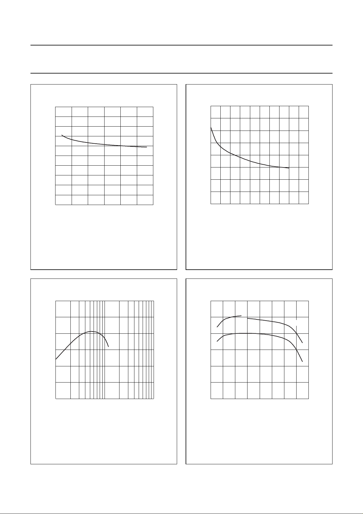
100
handbook, halfpage
h
FE
80
60
40
20
0
0 50 100 150
VCE=2V.
MGR624
IC (mA)
Fig.3 DC current gain as a function of collector
current; typical values.
800
handbook, halfpage
C
re
(fF)
600
400
200
0
0
IC= 0; f= 1 MHz.
15
234
VCB (V)
Fig.4 Feedback capacitance as a function of
collector-base voltage; typical values.
MGR625
30
handbook, halfpage
f
T
(GHz)
20
10
0
10 10
f = 2 GHz; VCE= 2 V; T
amb
=25°C.
2
IC (mA)
Fig.5 Transition frequency as a function of
collector current; typical values.
MGR626
120
G
max
IC (mA)
MGR627
30
handbook, halfpage
gain
(dB)
20
10
3
10
0
f = 900 MHz; VCE=2V.
MSG
S
21
0 40 80 160
Fig.6 Gain as a function of collector current;
typical values.
1998 Oct 21 5
 Loading...