

Philips BFG11W-X Datasheet

DISCRETE SEMICONDUCTORS
DATA SH EET
BFG11W/X
NPN 2 GHz power transistor
Product specification
Supersedes data of September 1995
File under Discrete Semiconductors, SC14
1996 Jun 04
Philips Semiconductors Product specification
NPN 2 GHz power transistor BFG11W/X
FEATURES
• High power gain
• High efficiency
• Small size discrete power amplifier
• 1.9 GHz operating area
• Gold metallization ensures excellent reliability
• Linear and non-linear operation.
APPLICATIONS
• Common emitter class-AB operation in handheld radio
equipment at 1.9 GHz such as DECT, PHS.
• Driver for DCS 1800.
DESCRIPTION
NPN silicon planar epitaxial transistor encapsulated in a
plastic 4-pin dual-emitter SOT343 package.
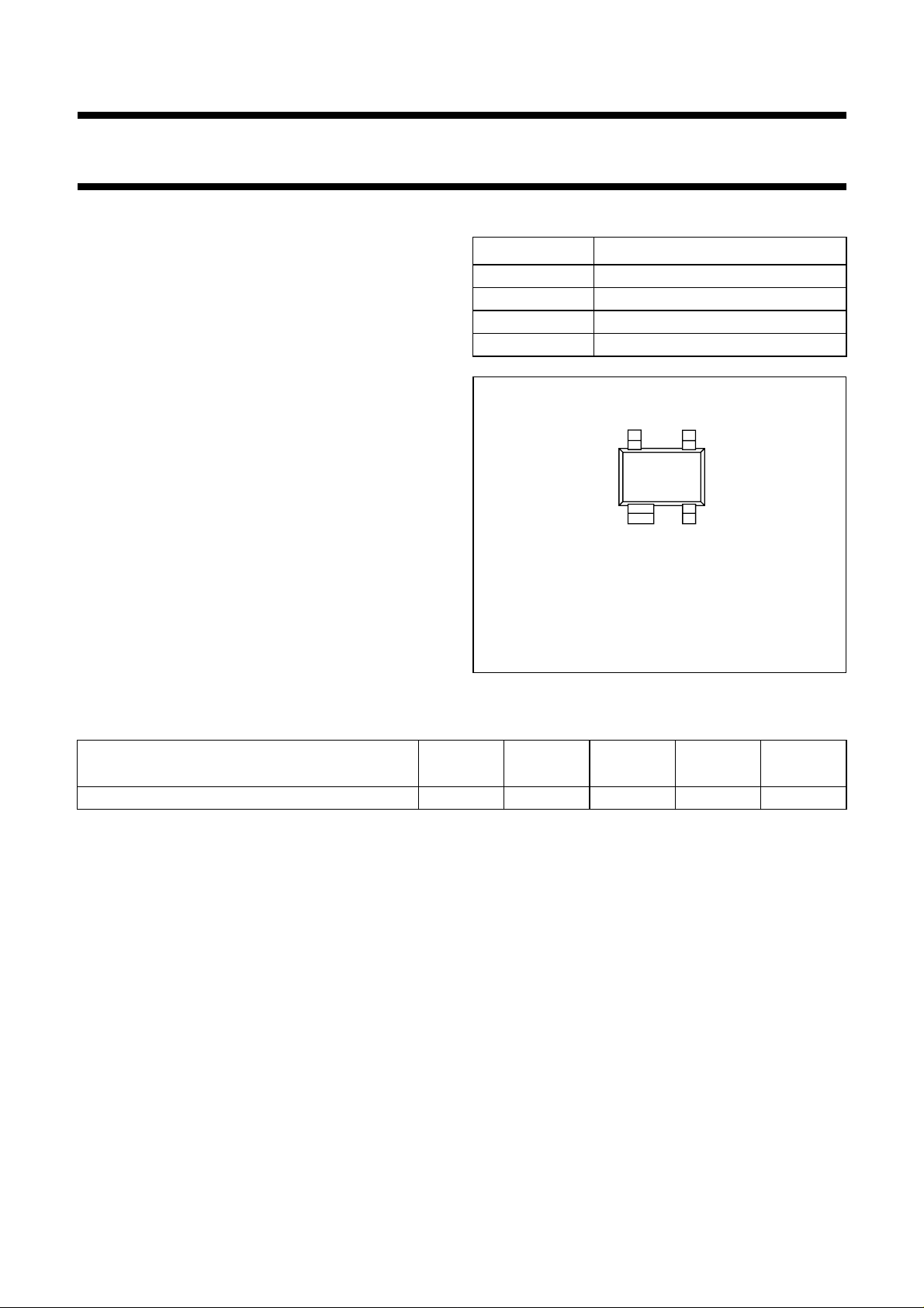
PINNING - SOT343
PIN DESCRIPTION
1 collector
2 emitter
3 base
4 emitter
handbook, halfpage
Marking code: S4
Fig.1 Simplified outline.
Top view
34
21
MBK523
QUICK REFERENCE DATA
RF performance at T
≤ 60 °C in a common-emitter test circuit.
s
MODE OF OPERATION
Pulsed, class-AB, δ < 1 : 2; t
f
(GHz)
= 5 ms 1.9 3.6 400 ≥6 ≥60
p
V
(V)
CE
P
L
(mW)
G
(dB)
p
η
(%)
c
1996 Jun 04 2
Philips Semiconductors Product specification
NPN 2 GHz power transistor BFG11W/X
LIMITING VALUES
In accordance with the Absolute Maximum Rating System (IEC 134).
SYMBOL PARAMETER CONDITIONS MIN. MAX. UNIT
V
CBO
V
CEO
V
EBO
I
C
P
tot
T
stg
T
j
THERMAL CHARACTERISTICS
SYMBOL PARAMETER CONDITIONS VALUE UNIT
R
th j-s
collector-base voltage open emitter − 20 V
collector-emitter voltage open base − 8V
emitter-base voltage open collector − 2.5 V
collector current (DC) − 500 mA
total power dissipation up to Ts=60°C; note 1 − 760 mW
storage temperature −65 +150 °C
junction temperature − 175 °C
thermal resistance from junction to soldering point up to Ts=60°C;
P
= 760 mW; note 1
tot
150 K/W
Note to the Limiting values and Thermal characteristics
1. T
is the temperature at the soldering point of the collector tab.
s
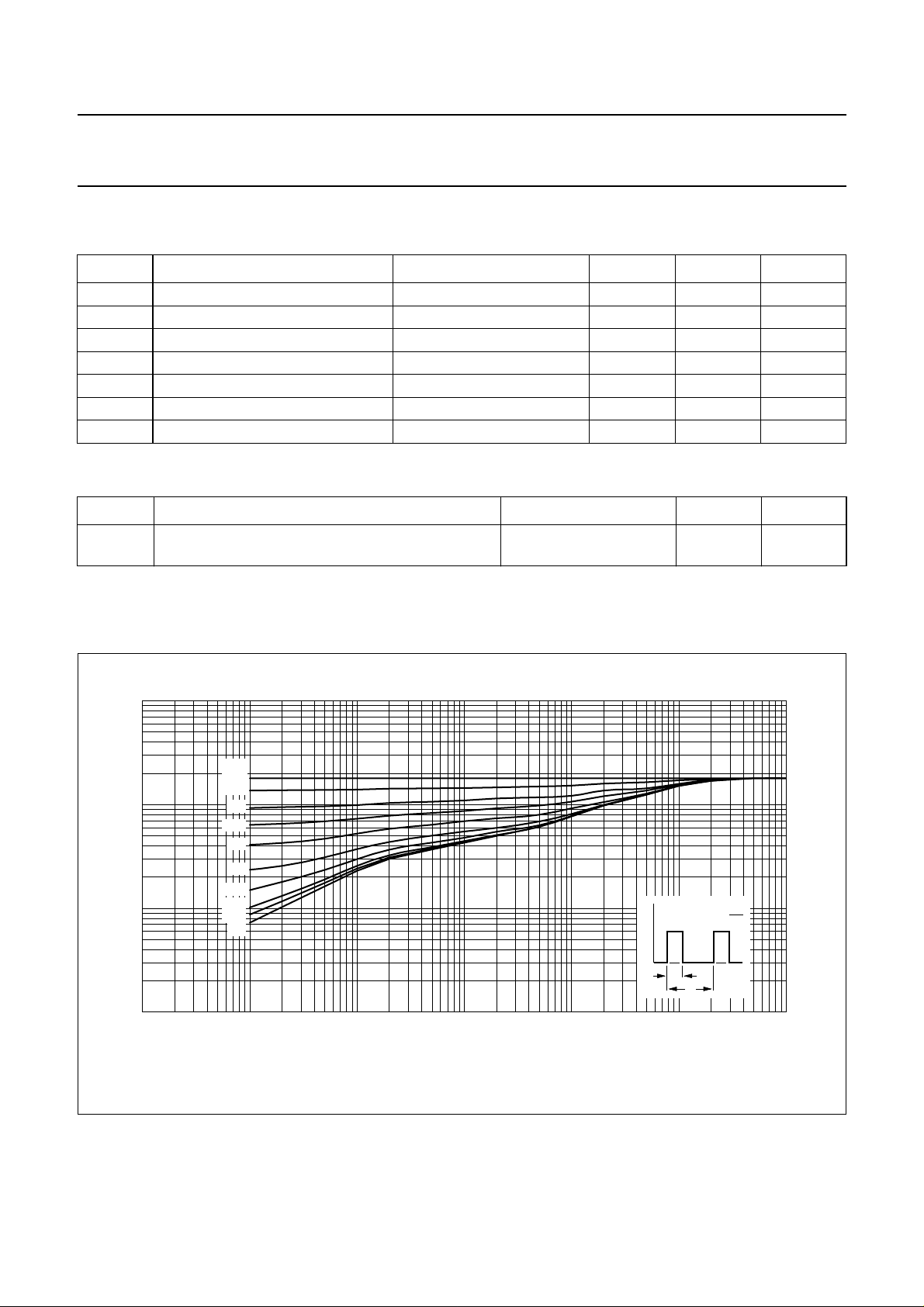
3
10
handbook, full pagewidth
Z
th j-s
(K/W)
2
10
10
1
−6
10
δ =
1
0.75
0.5
0.33
0.2
0.1
0.05
0.02
0.01
0.1
−5
10
−4
10
MGD411
t
P
t
p
T
−3
10
−2
10
−1
10
p
=
δ
T
t
tp (s)
1
Fig.2 Transient thermal impedance from junction to soldering point as a function of pulse time; typical values.
1996 Jun 04 3
Philips Semiconductors Product specification
NPN 2 GHz power transistor BFG11W/X
CHARACTERISTICS
T
=25°C unless otherwise specified.
j
SYMBOL PARAMETER CONDITIONS MIN. MAX. UNIT
V
(BR)CBO
V
(BR)CEO
V
(BR)EBO
I
CES
h
FE
C
c
C
re
APPLICATION INFORMATION
RF performance at T
collector-base breakdown voltage IC= 0.1 mA; open emitter 20 − V
collector-emitter breakdown voltage IC= 10 mA; open base 8 − V
emitter-base breakdown voltage IE= 0.1 mA; open collector 2.5 − V
collector cut-off current VCE=8V; VBE=0 − 100 µA
DC current gain VCE=5V; IC= 100 mA 25 −
collector capacitance VCB= 3.6 V; IE=ie= 0; f = 1 MHz − 5pF
feedback capacitance VCE= 3.6 V; IC= 0; f = 1 MHz − 4pF
≤ 60 °C in a common-emitter test circuit.
s
MODE OF OPERATION
Pulsed, class-AB, δ < 1 : 2; t
f
(GHz)
= 5 ms 1.9 3.6 1 400 ≥6 ≥60
p
V
CE
(V)
I
CQ
(mA)
P
L
(mW)
G
(dB)
p
η
c
(%)
Ruggedness in class-AB operation
The transistors are capable of withstanding a load mismatch corresponding to VSWR =8:1 through all phases, at rated
output power under pulsed conditions at f = 1.9 GHz: t
= 1.25 ms, δ =1:8 atVCE= 7 V and tp= 5 ms, δ =1:2 at
p
VCE= 4.5 V.
G
(dB)
8
p
6
4
2
handbook, halfpage
MGD412
90
η
G
p
η
C
(%)
70
50
30
C
handbook, halfpage
0
d
im
(dBc)
−20
d
im
−40
−60
η
c
MGD552
80
η
(%)
60
40
20
c
0
0 200 400 800
VCE= 3.6V; VBE= 0.65 V; f = 1.9 GHz; δ < 1 : 8; tp= 1.25 ms.
600
PL (mW)
10
Fig.3 Power gain and efficiency as functions
of load power; typical values.
1996 Jun 04 4
−80
030
VCE= 3.6 V; Icϕ= 1 mA; f1= 1990.0 MHz;
= 1990.1 MHz; δ = 1 : 8; tp= 625 µs.
f
2
10 20
P
o(av)
0
(dBm)
Fig.4 Two tone intermodulation distortion
and efficiency as functions of average
output power; typical values.
 Loading...