

Philips BF1100R, BF1100 Datasheet

DISCRETE SEMICONDUCTORS
DATA SH EET
BF1100; BF1100R
Dual-gate MOS-FETs
Product specification
File under Discrete Semiconductors, SC07
Philips Semiconductors
1995 Apr 25
Philips Semiconductors Product specification
Dual-gate MOS-FETs BF1100; BF1100R
FEATURES
• Specially designed for use at 9 to 12 V supply voltage
• Short channel transistor with high forward transfer
admittance to input capacitance ratio
• Low noise gain controlled amplifier up to 1 GHz
• Superior cross-modulation performance during AGC.
APPLICATIONS
• VHF and UHF applications such as television tuners and
professional communications equipment.
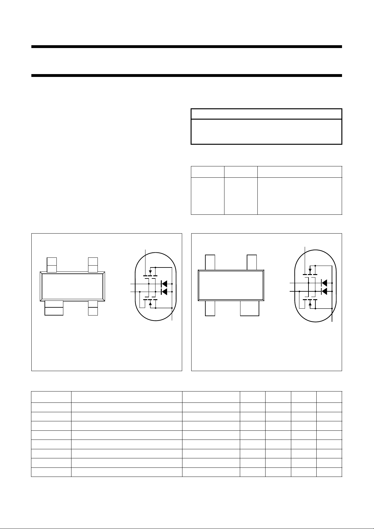
DESCRIPTION
Enhancement type field-effect transistor in a plastic
microminiature SOT143 or SOT143R package. The
transistor consists of an amplifier MOS-FET with source
handbook, halfpage
43
d
and substrate interconnected and an internal bias circuit to
ensure good cross-modulation performance during AGC.
CAUTION
The device is supplied in an antistatic package. The
gate-source input must be protected against static
discharge during transport or handling.
PINNING
PIN SYMBOL DESCRIPTION
1 s, b source
2 d drain
3g
4g
handbook, halfpage
34
gate 2
2
gate 1
1
d
g
2
g
1
21
Top view
BF1100 marking code: M56.
MAM124
Fig.1 Simplified outline (SOT143) and symbol.
s,b
12
Top view
BF1100R marking code: M57.
MAM125 - 1
Fig.2 Simplified outline (SOT143R) and symbol.
g
2
g
1
QUICK REFERENCE DATA
SYMBOL PARAMETER CONDITIONS MIN. TYP. MAX. UNIT
V
DS
I
D
P
tot
T
j
forward transfer admittance 24 28 33 mS
y
fs
C
ig1-s
C
rs
drain-source voltage −−14 V
drain current −−30 mA
total power dissipation −−200 mW
operating junction temperature −−150 °C
input capacitance at gate 1 − 2.2 2.6 pF
reverse transfer capacitance f=1MHz − 25 35 fF
F noise figure f = 800 MHz − 2 − dB
s,b
1995 Apr 25 2
Philips Semiconductors Product specification
Dual-gate MOS-FETs BF1100; BF1100R
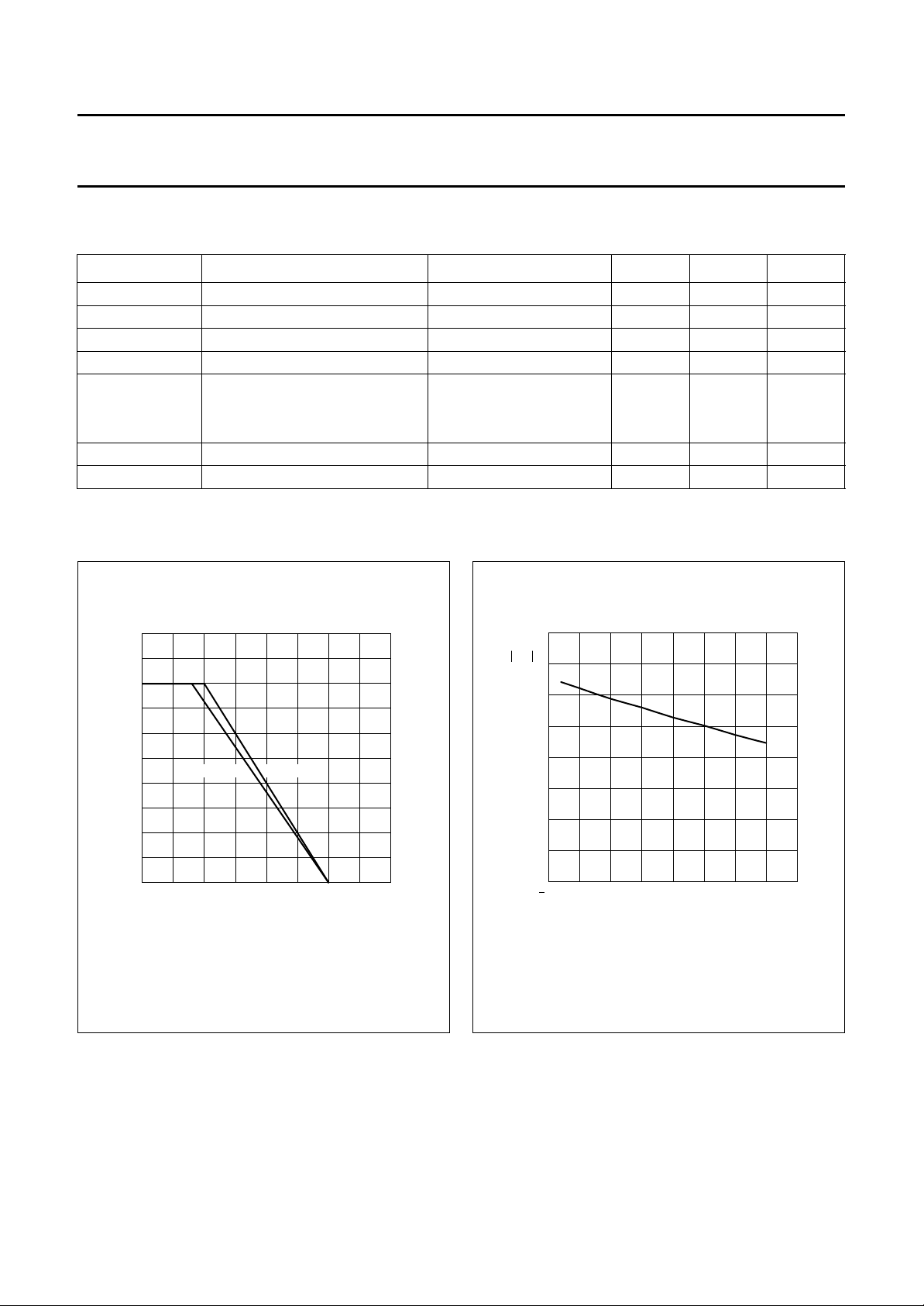
LIMITING VALUES
In accordance with the Absolute Maximum Rating System (IEC 134).
SYMBOL PARAMETER CONDITIONS MIN. MAX. UNIT
V
DS
I
D
I
G1
I
G2
P
tot
T
stg
T
j
Note
1. Device mounted on a printed-circuit board.
drain-source voltage − 14 V
drain current − 30 mA
gate 1 current −±10 mA
gate 2 current −±10 mA
total power dissipation see Fig.3
BF1100 up to T
BF1100R up to T
=50°C; note 1 − 200 mW
amb
=40°C; note 1 − 200 mW
amb
storage temperature −65 +150 °C
operating junction temperature − +150 °C
250
handbook, halfpage
P
tot
(mW)
200
150
100
50
0
0 50 100 200
BF1100R BF1100
150
T ( C)
amb
Fig.3 Power derating curves.
MLD155
o
100
MLD156
o
T ( C)
j
40
Y
fs
(mS)
30
20
10
0
50 0 50 150
Fig.4 Forward transfer admittance as a function
of junction temperature; typical values.
1995 Apr 25 3

Philips Semiconductors Product specification
Dual-gate MOS-FETs BF1100; BF1100R
THERMAL CHARACTERISTICS
SYMBOL PARAMETER CONDITIONS VALUE UNIT
R
th j-a
R
th j-s
Notes
1. Device mounted on a printed-circuit board.
is the temperature at the soldering point of the source lead.
2. T
s
STATIC CHARACTERISTICS
=25°C; unless otherwise specified.
T
j
thermal resistance from junction to ambient note 1
BF1100 500 K/W
BF1100R 550 K/W
thermal resistance from junction to soldering point note 2
BF1100 T
BF1100R T
=92°C 290 K/W
s
=78°C 360 K/W
s
SYMBOL PARAMETER CONDITIONS MIN. MAX. UNIT
V
(BR)G1-SS
V
(BR)G2-SS
V
(F)S-G1
V
(F)S-G2
V
G1-S(th)
gate 1-source breakdown voltage V
gate 2-source breakdown voltage V
forward source-gate 1 voltage V
forward source-gate 2 voltage V
gate 1-source threshold voltage V
G2-S=VDS
G1-S=VDS
G2-S=VDS
G1-S=VDS
G2-S
= 0; I
= 0; I
= 0; I
= 0; I
=4V; VDS=9V;
= 1 mA 13.2 20 V
G1-S
= 1 mA 13.2 20 V
G2-S
= 10 mA 0.5 1.5 V
S-G1
= 10 mA 0.5 1.5 V
S-G2
0.3 1 V
ID=20µA
=4V; VDS=12V;
V
G2-S
0.3 1 V
ID=20µA
V
G2-S(th)
gate 2-source threshold voltage V
=4V; VDS=9V;
G1-S
0.3 1.2 V
ID=20µA
=4V; VDS=12V;
V
G1-S
0.3 1.2 V
ID=20µA
I
DSX
drain-source current V
=4V; VDS=9V;
G2-S
813mA
RG1= 180 kΩ; note 1
I
G1-SS
I
G2-SS
gate 1 cut-off current V
gate 2 cut-off current V
V
=4V; VDS=12V;
G2-S
= 250 kΩ; note 2
R
G1
G2-S=VDS
G1-S=VDS
= 0; V
= 0; V
=12V − 50 nA
G1-S
=12V − 50 nA
G2-S
813mA
Notes
1. R
connects gate 1 to VGG= 9 V; see Fig.27.
G1
2. RG1 connects gate 1 to VGG= 12 V; see Fig.27.
1995 Apr 25 4
Philips Semiconductors Product specification
Dual-gate MOS-FETs BF1100; BF1100R
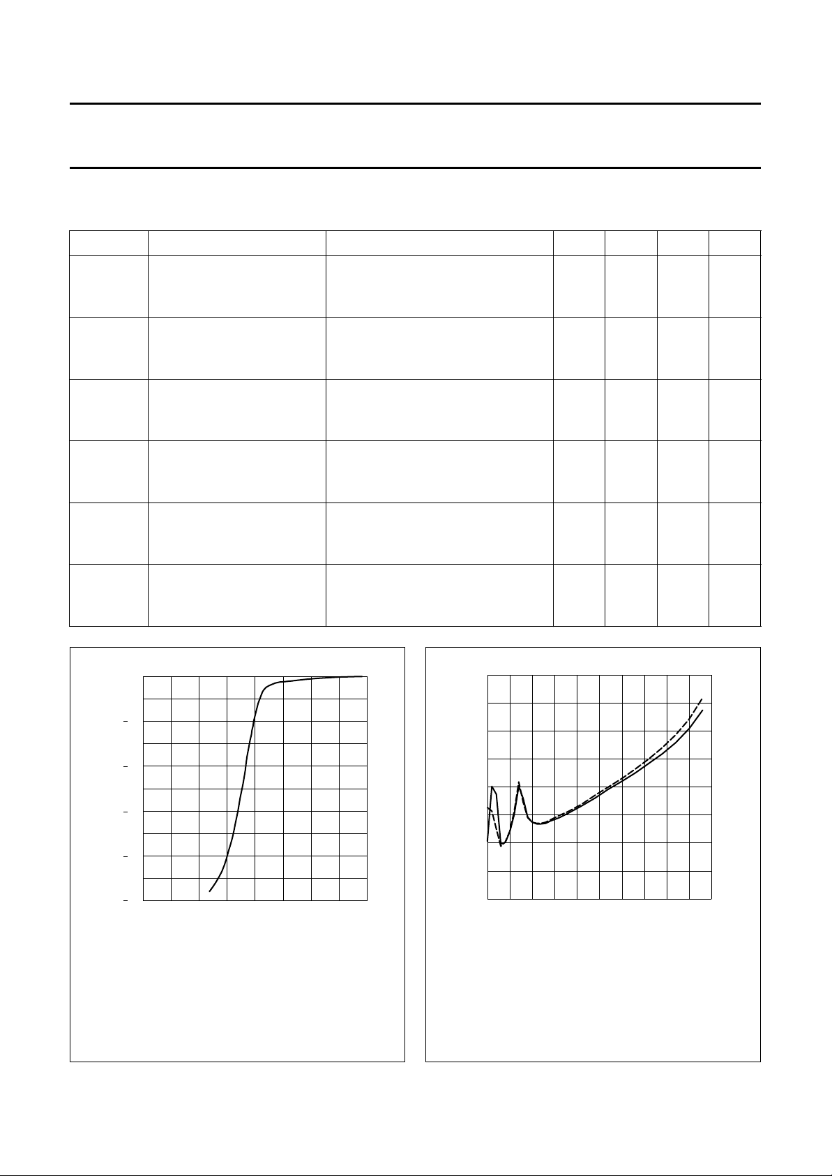
DYNAMIC CHARACTERISTICS
Common source; T
SYMBOL PARAMETER CONDITIONS MIN. TYP. MAX. UNIT
y
forward transfer admittance pulsed; Tj=25°C
fs
C
C
C
C
ig1-s
ig2-s
os
rs
input capacitance at gate 1 f = 1 MHz
input capacitance at gate 2 f = 1 MHz
drain-source capacitance f = 1 MHz
reverse transfer capacitance f = 1 MHz
F noise figure f = 800 MHz; G
=25°C; V
amb
= 4 V; ID= 10 mA; unless otherwise specified.
G2-S
= 9 V 24 28 33 mS
V
DS
= 12 V 24 28 33 mS
V
DS
=9V − 2.2 2.6 pF
V
DS
=12V − 2.2 2.6 pF
V
DS
=9V − 1.6 − pF
V
DS
=12V − 1.4 − pF
V
DS
=9V − 1.4 1.8 pF
V
DS
=12V − 1.1 1.5 pF
V
DS
=9V − 25 35 fF
V
DS
=12V − 25 35 fF
V
DS
S=GSopt
; BS=B
VDS=9V − 2 2.8 dB
=12V − 2 2.8 dB
V
DS
Sopt
0
handbook, halfpage
gain
reduction
(dB)
10
20
30
40
50
01234
f =50 MHz.
Tj=25°C.
V (V)
AGC
Fig.5 Gain reduction as a function of the AGC
voltage; typical values.
MLD157
120
handbook, halfpage
V
unw
(dBµV)
110
100
90
80
0
10 20 30 40 50
(1) RG= 250 kΩ to VGG=12V
(2) RG= 180 kΩ to VGG=9V
fw= 50 MHz; f
= 60 MHz; T
unw
amb
gain reduction (dB)
=25°C.
MLD158
(1)
(2)
Fig.6 Unwanted voltage for 1% cross-modulation
as a function of gain reduction; typical
values; see Fig.27.
1995 Apr 25 5
 Loading...