

Philips BD830 Datasheet
DATA SH EET
Product specification
Supersedes data of 1998 May 29
1999 Apr 21
DISCRETE SEMICONDUCTORS
BD830
PNP power transistor
ook, halfpage
M3D067
1999 Apr 21 2
Philips Semiconductors Product specification
PNP power transistor BD830
FEATURES
• High current (max. 1 A)
• Low voltage (max. 80 V).
APPLICATIONS
• General purpose
• Driver stages in hi-fi amplifiers and television circuits.
DESCRIPTION
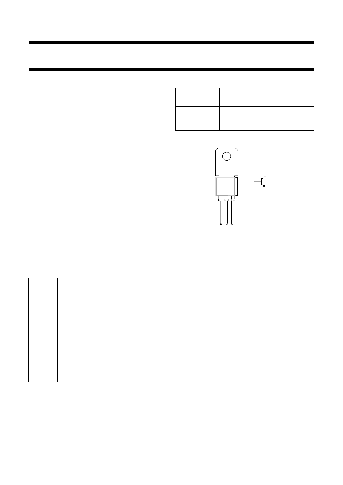
PNP power transistor in a TO-202; SOT128B plastic
package. NPN complement: BD829.
PINNING
PIN DESCRIPTION
1 emitter
2 collector, connected to metal part of
mounting surface
3 base
Fig.1 Simplified outline (TO-202; SOT128B)
and symbol.
handbook, halfpage
2
1
3
MAM304
123
LIMITING VALUES
In accordance with the Absolute Maximum Rating System (IEC 134).
SYMBOL PARAMETER CONDITIONS MIN. MAX. UNIT
V
CBO
collector-base voltage open emitter −−100 V
V
CEO
collector-emitter voltage open base −−80 V
V
EBO
emitter-base voltage open collector −−5V
I
C
collector current (DC) −−1A
I
CM
peak collector current −−1.5 A
I
BM
peak base current −−500 mA
P
tot
total power dissipation T
amb
≤ 25 °C − 2W
T
mb
≤ 50 °C − 8W
T
stg
storage temperature −65 +150 °C
T
j
junction temperature − 150 °C
T
amb
operating ambient temperature −65 +150 °C
1999 Apr 21 3
Philips Semiconductors Product specification
PNP power transistor BD830
THERMAL CHARACTERISTICS
CHARACTERISTICS
T
j
=25°C unless otherwise specified.
SYMBOL PARAMETER CONDITIONS VALUE UNIT
R
th j-a
thermal resistance from junction to ambient in free air 62.5 K/W
R
th j-mb
thermal resistance from junction to mounting base 12.5 K/W
SYMBOL P ARAMETER CONDITIONS MIN. TYP. MAX. UNIT
I
CBO
collector cut-off current IE= 0; VCB= −30 V −−−100 nA
I
E
= 0; VCB= −30 V; Tj= 125 °C −−−10 µA
I
EBO
emitter cut-off current IC= 0; VEB= −5V −−−100 nA
h
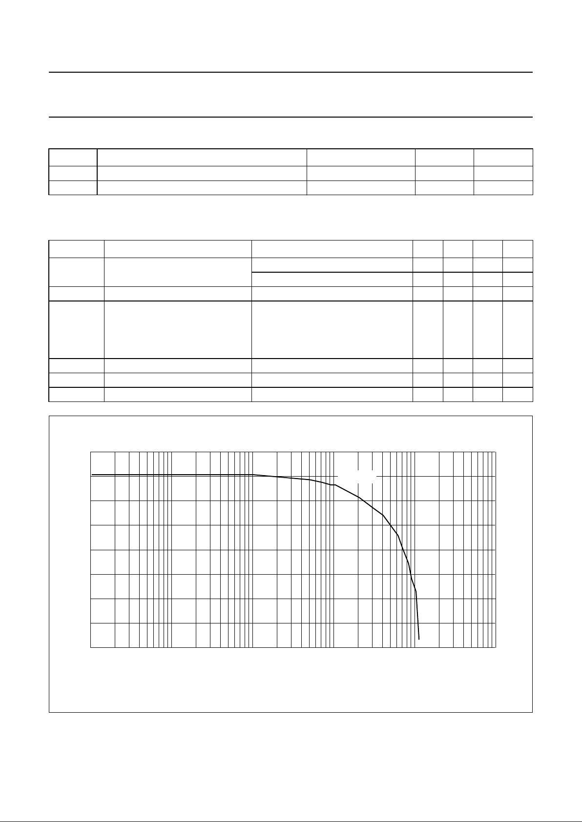
FE
DC current gain VCE= −2 V; see Fig.2
I
C
= −5mA 40 −−
I
C
=−150 mA 63 − 250
I
C
= −500 mA 25 −−
V
CEsat
collector-emitter saturation voltage IC= −500 mA; IB= −50 mA −−−500 mV
V
BE
base-emitter voltage IC= −500 mA; VCE= −2V −−−1V
f
T
transition frequency IC= −50 mA; VCE= −5 V; f = 100 MHz − 75 − MHz
Fig.2 DC current gain; typical values.
handbook, full pagewidth
0
160
80
120
40
MBH730
−10
−1
h
FE
−1
IC (mA)
−10 −10
3
−10
4
−10
2
VCE = −2 V
 Loading...