

Philips BD329 Datasheet
DISCRETE SEMICONDUCTORS
DATA SH EET
ook, halfpage
M3D100
BD329
NPN power transistor
Product specification
Supersedes data of September 1994
File under Discrete Semiconductors, SC04
1997 Mar 07
Philips Semiconductors Product specification
NPN power transistor BD329
FEATURES
• High current (max. 3 A)
• Low voltage (max. 20 V).
APPLICATIONS
• Especially for battery equipped applications.
DESCRIPTION
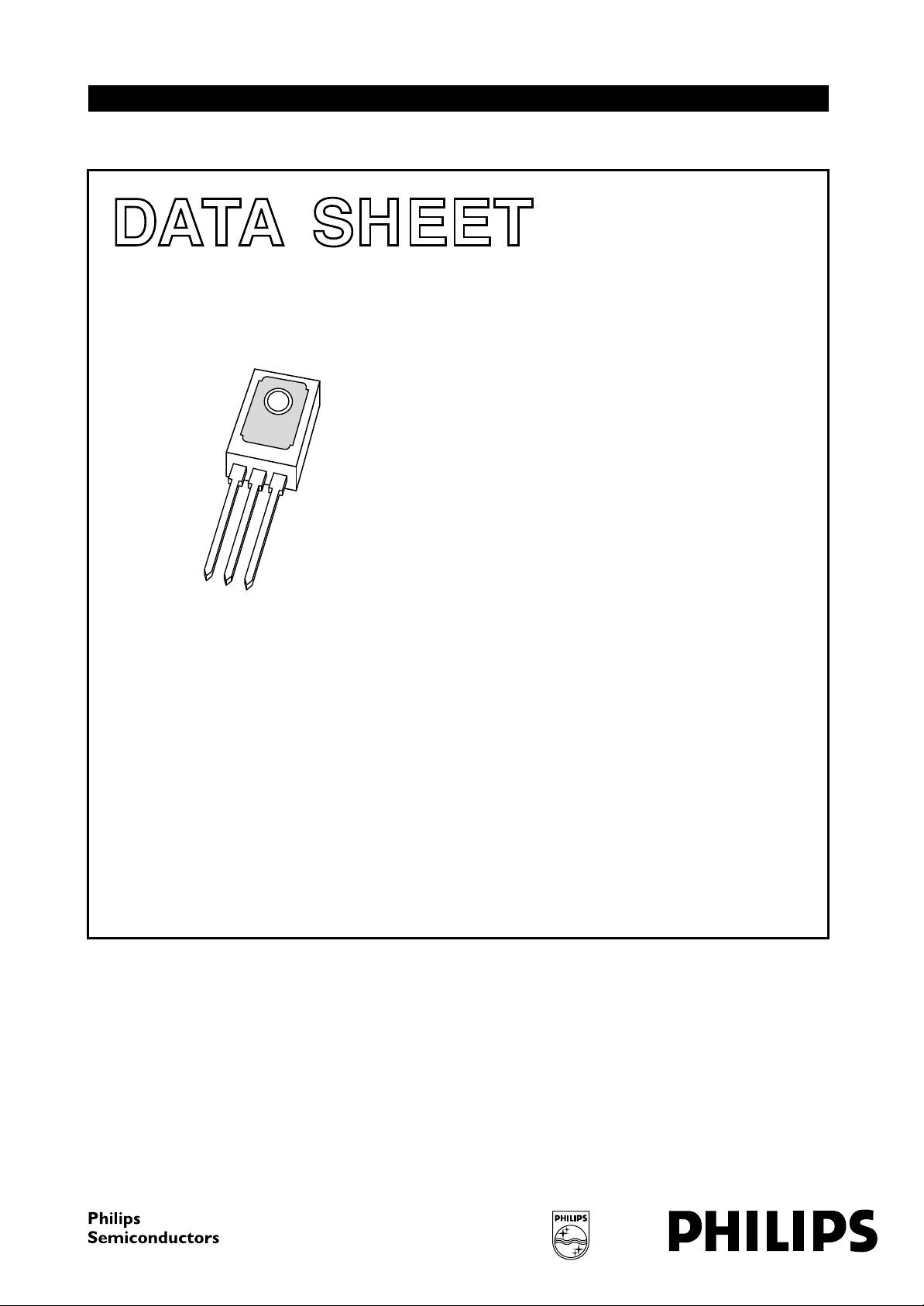
NPN power transistor in a TO-126; SOT32 plastic
package. PNP complement: BD330.
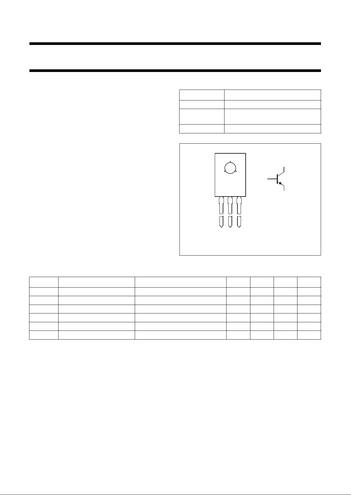
PINNING
PIN DESCRIPTION
1 emitter
2 collector, connected to metal part of
mounting surface
3 base
handbook, halfpage
123
Top view
Fig.1 Simplified outline (TO-126; SOT32)
and symbol.
2
3
1
MAM254
QUICK REFERENCE DATA
SYMBOL PARAMETER CONDITIONS MIN. TYP. MAX. UNIT
V
CBO
V
CEO
I
CM
P
tot
h
FE
f
T
collector-base voltage open emitter −−32 V
collector-emitter voltage open base −−20 V
peak collector current −−3A
total power dissipation Tmb≤ 45 °C −−15 W
DC current gain IC= 0.5 A; VCE=1V 85 − 375
transition frequency IC= 50 mA; VCE= 5 V; f = 100 MHz − 130 − MHz
1997 Mar 07 2

Philips Semiconductors Product specification
NPN power transistor BD329
LIMITING VALUES
In accordance with the Absolute Maximum Rating System (IEC 134).
SYMBOL PARAMETER CONDITIONS MIN. MAX. UNIT
V
CBO
V
CEO
V
EBO
I
C
I
CM
I
BM
P
tot
T
stg
T
j
T
amb
collector-base voltage open emitter − 32 V
collector-emitter voltage open base − 20 V
emitter-base voltage open collector − 5V
collector current (DC) − 3A
peak collector current − 3A
peak base current − 1A
total power dissipation Tmb≤ 45 °C − 15 W
storage temperature −65 +150 °C
junction temperature − 150 °C
operating ambient temperature −65 +150 °C
THERMAL CHARACTERISTICS
SYMBOL PARAMETER CONDITIONS VALUE UNIT
R
th j-a
R
th j-mb
thermal resistance from junction to ambient note1 100 K/W
thermal resistance from junction to mounting base 7 K/W
Note
1. Refer to TO-126; SOT32 standard mounting conditions.
1997 Mar 07 3
 Loading...