

Philips BD230 Datasheet
DISCRETE SEMICONDUCTORS
DATA SH EET
ook, halfpage
M3D100
BD230
NPN power transistor
Product specification
Supersedes data of 1997 Mar 06
1999 Apr 21

Philips Semiconductors Product specification
NPN power transistor BD230
FEATURES
• High current (max. 1.5 A)
• Low voltage (max. 80 V).
APPLICATIONS
• Driver stages in television circuits.
DESCRIPTION
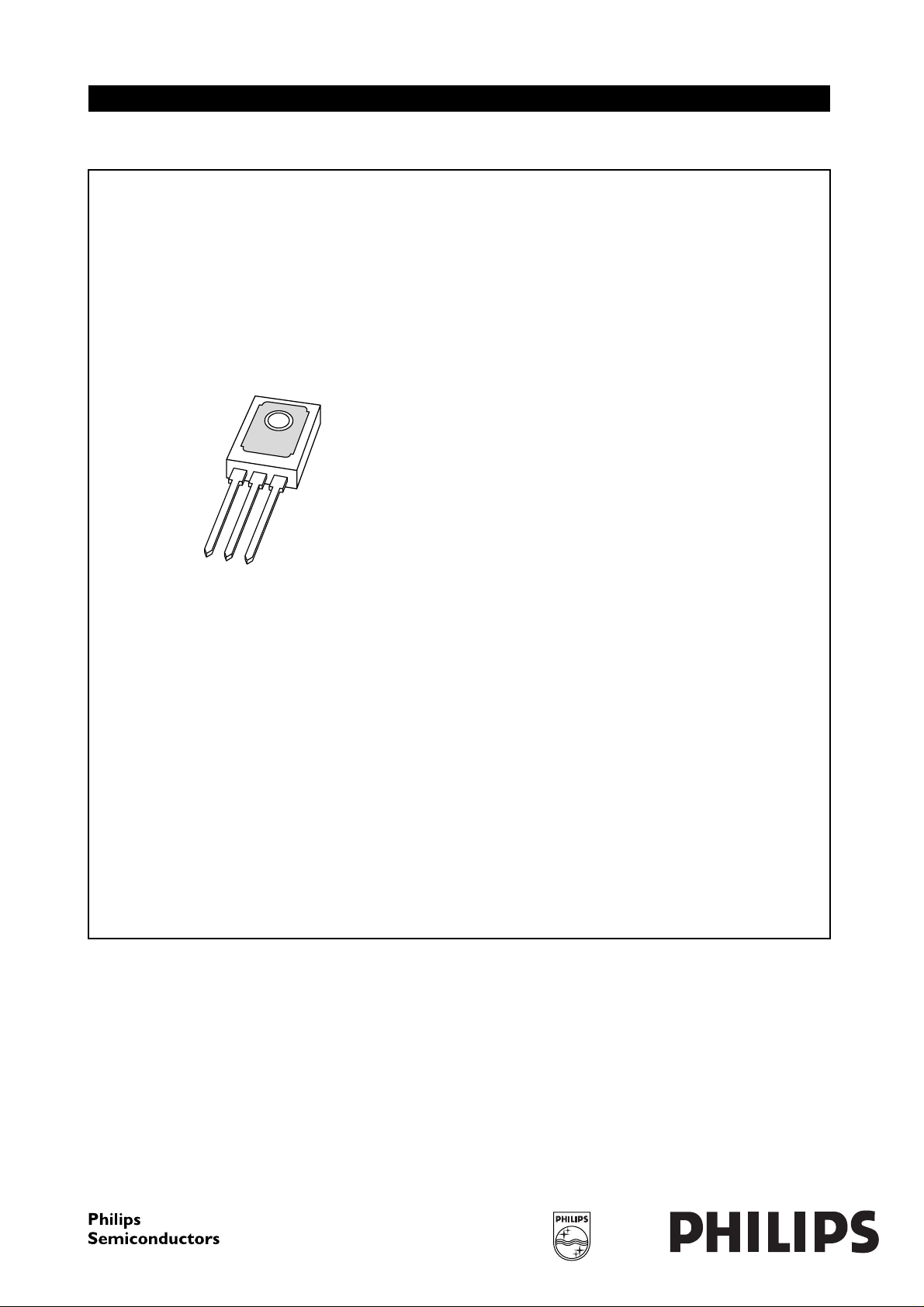
NPN power transistor in a TO-126; SOT32 plastic
package. PNP complement: BD231.
PINNING
PIN DESCRIPTION
1 emitter
2 collector, connected to metal part of
mounting surface
3 base
handbook, halfpage
3
123
Top view
Fig.1 Simplified outline (TO-126; SOT32)
and symbol.
2
1
MAM254
LIMITING VALUES
In accordance with the Absolute Maximum Rating System (IEC 134).
SYMBOL PARAMETER CONDITIONS MIN. MAX. UNIT
V
CBO
V
CEO
V
EBO
I
C
I
CM
I
BM
P
tot
T
stg
T
j
T
amb
collector-base voltage open emitter − 100 V
collector-emitter voltage open base − 80 V
emitter-base voltage open collector − 5V
collector current (DC) − 1.5 A
peak collector current − 3A
peak base current − 1A
total power dissipation Tmb≤ 62 °C − 12.5 W
storage temperature −65 +150 °C
junction temperature − 150 °C
operating ambient temperature −65 +150 °C
1999 Apr 21 2

Philips Semiconductors Product specification
NPN power transistor BD230
THERMAL CHARACTERISTICS
SYMBOL PARAMETER CONDITIONS VALUE UNIT
R
th j-a
R
th j-mb
Note
1. Refer to TO-126; SOT32 standard mounting conditions.
CHARACTERISTICS
=25°C unless otherwise specified.
T
j
SYMBOL P ARAMETER CONDITIONS MIN. TYP. MAX. UNIT
I
CBO
I
EBO
h
FE
V
CEsat
V
BEsat
V
BE
f
T
h
FE1
----------h
FE2
thermal resistance from junction to ambient note 1 100 K/W
thermal resistance from junction to mounting base 7 K/W
collector cut-off current IE= 0; VCB=30V −− 100 nA
I
= 0; VCB= 30 V; Tj= 125 °C −− 10 µA
E
emitter cut-off current IC= 0; VEB=5V −− 100 nA
DC current gain VCE= 2 V; see Fig.2
= 5 mA 40 −−
I
C
I
= 150 mA 40 − 250
C
I
=1A 25 −−
C
collector-emitter saturation voltage IC= 1 A; IB= 0.1 A −− 0.8 V
base-emitter saturation voltage IC= 1 A; IB= 0.1 A −− 1.2 V
base-emitter voltage IC= 1 A; VCE= 2 V; note 1 −− 1.3 V
transition frequency IC= 50 mA; VCE= 5 V; f = 100 MHz − 125 − MHz
DC current gain ratio of the
I
= 150 mA; VCE =2V − 1.3 1.6
C
complementary pairs
Note
1. V
decreases by about 2.3 mV/K with increasing temperature.
BE
1999 Apr 21 3
 Loading...