

Philips BC817DS Technical data
查询BC817DS供应商查询BC817DS供应商
DISCRETE SEMICONDUCTORS
DATA SH EET
ook, halfpage
M3D302
BC817DS
NPN general purpose double
transistor
Product specification
Supersedes data of 2002 Aug 09
2002 Nov 22
Philips Semiconductors Product specification
NPN general purpose double transistor BC817DS
FEATURES
• High current (500 mA)
• 600 mW total power dissipation
• Replaces two SOT23 packaged transistors on same
PCB area.
APPLICATIONS
• General purpose switching and amplification
• Push-pull amplifiers
• Multi-phase stepper motor drivers.
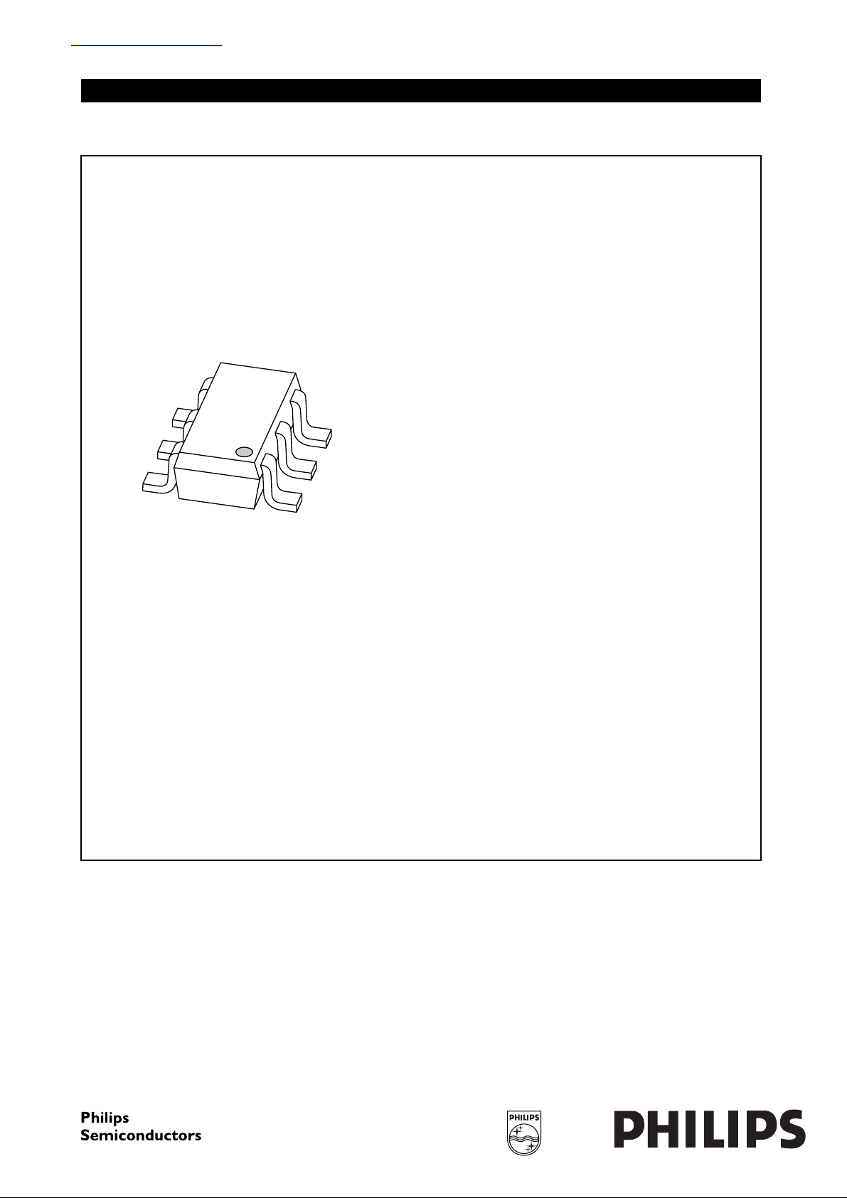
DESCRIPTION
NPN transistor pair in a SOT457 (SC-74) plastic package.
MARKING
TYPE NUMBER MARKING CODE
BC817DS N3
QUICK REFERENCE DATA
SYMBOL PARAMETER MAX. UNIT
V
I
I
CEO
C
CM
collector-emitter voltage 45 V
collector current (DC) 500 mA
peak collector current 1 A
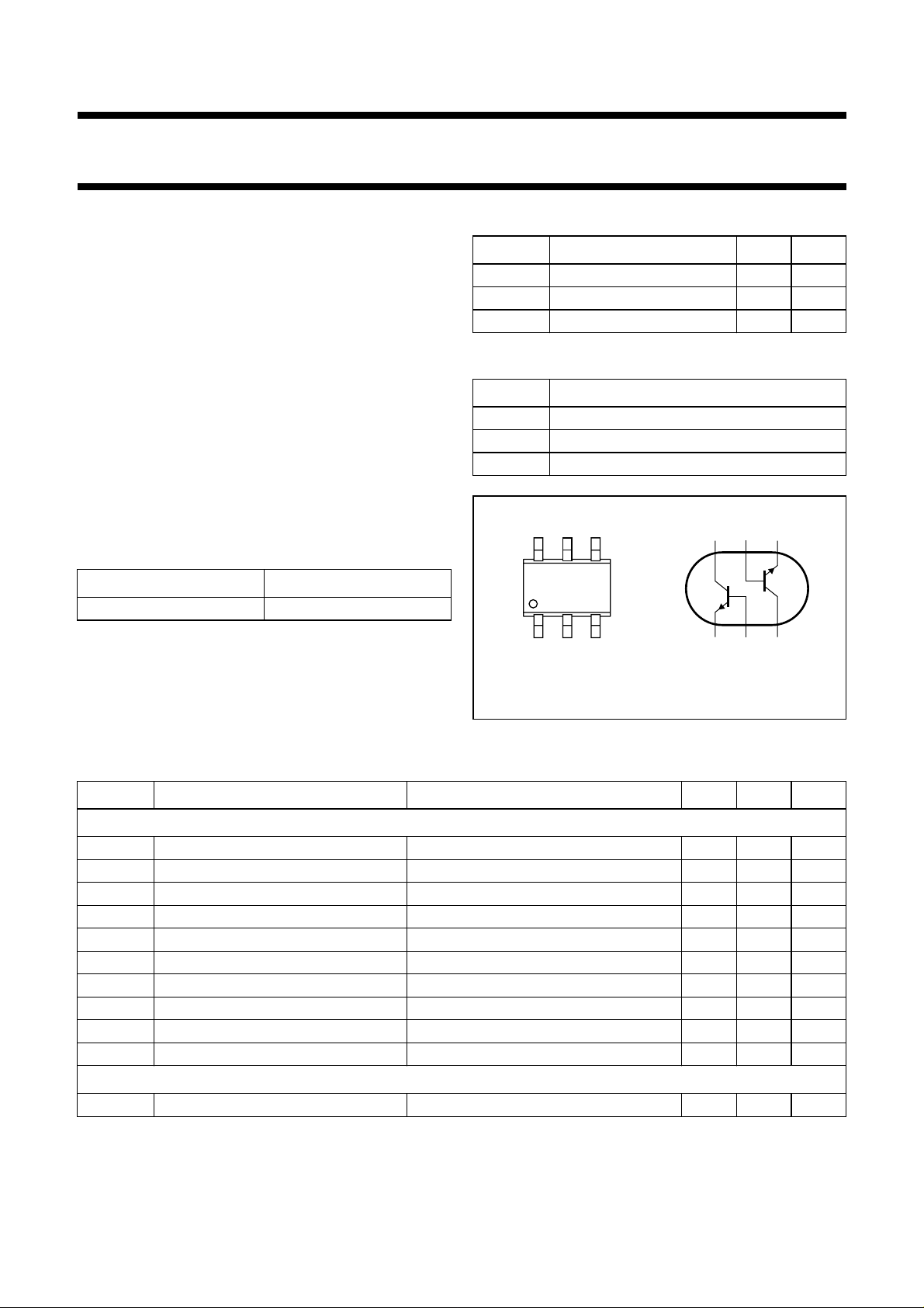
PINNING
PIN DESCRIPTION
1, 4 emitter TR1; TR2
2, 5 base TR1; TR2
6, 3 collector TR1; TR2
handbook, halfpage
Top view
4
56
132
MAM340
645
TR2
TR1
132
Fig.1 Simplified outline (SOT457) and symbol.
LIMITING VALUES
In accordance with the Absolute Maximum Rating System (IEC 60134).
SYMBOL PARAMETER CONDITIONS MIN. MAX. UNIT
Per transistor unless otherwise specified
V
CBO
V
CEO
V
EBO
I
C
I
CM
I
BM
P
tot
T
stg
T
j
T
amb
collector-base voltage open emitter − 50 V
collector-emitter voltage open base − 45 V
emitter-base voltage open collector − 5V
collector current (DC) − 500 mA
peak collector current − 1A
peak base current − 200 mA
total power dissipation T
≤ 25 °C; note 1 − 370 mW
amb
storage temperature −65 +150 °C
junction temperature − 150 °C
operating ambient temperature −65 +150 °C
Per device
P
tot
total power dissipation T
≤ 25 °C; note 1 − 600 mW
amb
Note
1. Device mounted on a printed-circuit board; single sided copper; tinplated; mounting pad for collector 1 cm2.
2002 Nov 22 2
Philips Semiconductors Product specification
NPN general purpose double transistor BC817DS
THERMAL CHARACTERISTICS
SYMBOL PARAMETER CONDITIONS VALUE UNIT
R
th j-a
thermal resistancefromjunction to
ambient
Note
1. Device mounted on a printed-circuit board; single sided copper; tinplated; mounting pad for collector 1 cm
CHARACTERISTICS
T
=25°C unless otherwise specified.
amb
SYMBOL PARAMETER CONDITIONS MIN. TYP. MAX. UNIT
Per transistor
I
CBO
I
EBO
h
FE
V
CEsat
V
BE
C
c
f
T
collector-base cut-off current VCB= 20 V; IE=0 −−100 nA
emitter-base cut-off current VEB=5V; IC=0 −−100 nA
DC current gain VCE=1V; IC= 100 mA; note 1 160 − 400
collector-emitter saturation voltage IC= 500 mA; IB= 50 mA; note 1 −−700 mV
base-emitter voltage VCE=1V; IC= 500 mA;
collector capacitance VCB= 10 V; IE=Ie= 0; f = 1 MHz − 5 − pF
transition frequency VCE=5V; IC= 10 mA;
note 1 208 K/W
2
.
= 20 V; IE= 0; Tj= 150 °C −−5µA
V
CB
V
=1V; IC= 500 mA; note 1 40 −−
CE
−−1.2 V
notes 1 and 2
100 −−MHz
f = 100 MHz
Notes
1. Pulse test: t
≤ 300 µs; δ≤0.02.
p
2. VBE decreases by approximately −2 mV/K with increasing temperature.
2002 Nov 22 3
 Loading...