

Philips BC807W, BC807-40W, BC807-16W Datasheet
DISCRETE SEMICONDUCTORS
DATA SH EET
ook, halfpage
M3D187
BC807W
PNP general purpose transistor
Product specification
Supersedes data of 1997 Jun 09
1999 May 18
Philips Semiconductors Product specification
PNP general purpose transistor BC807W
FEATURES
• High current (max. 500 mA)
• Low voltage (max. 45 V).
APPLICATIONS
• General purpose switching and amplification.
DESCRIPTION
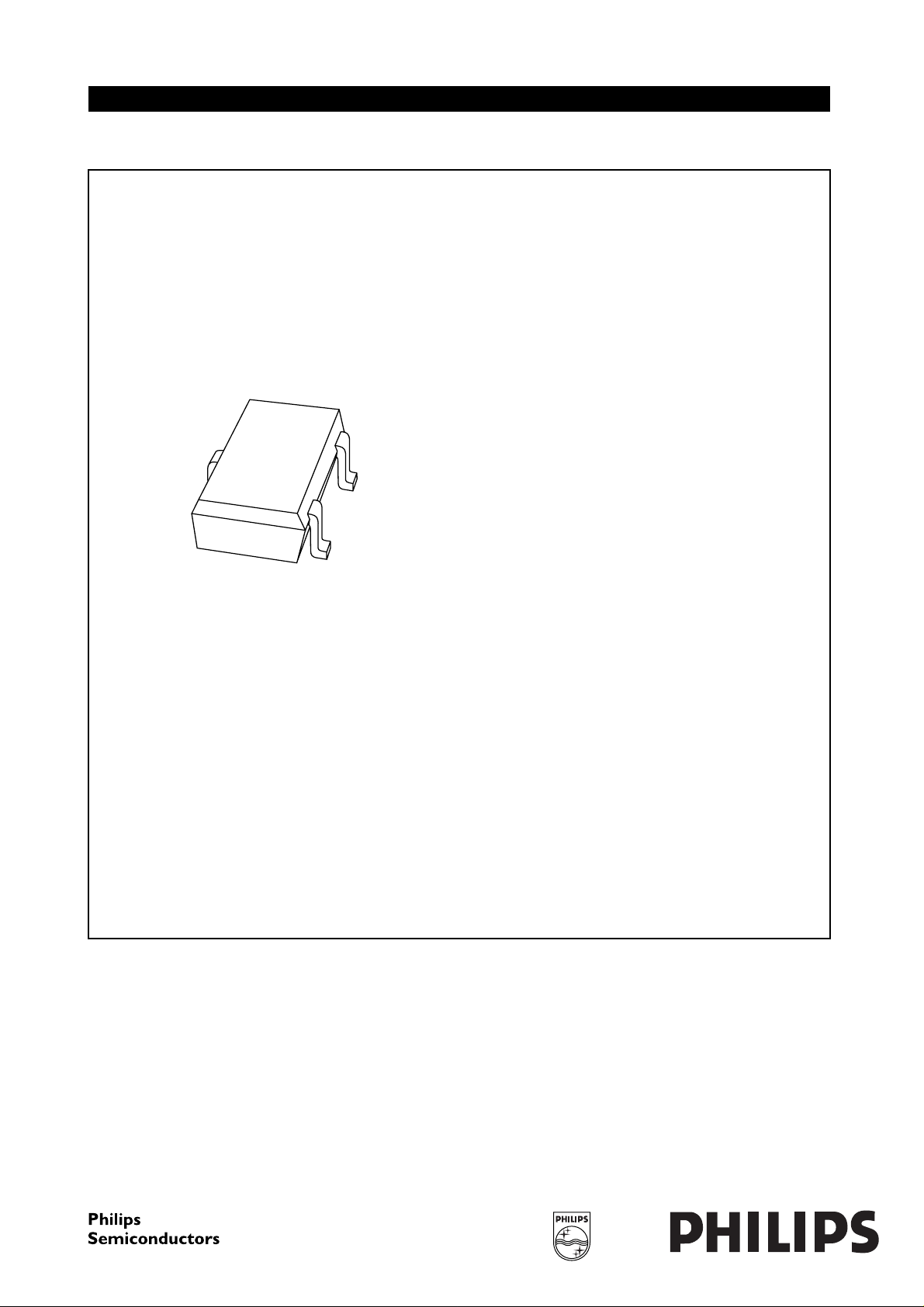
PNP transistor in a SOT323 plastic package.
NPN complement: BC817W.
MARKING
TYPE
NUMBER
MARKING
(1)
CODE
TYPE
NUMBER
MARKING
CODE
BC807W 5D∗ BC807-25W 5B∗
BC807-16W 5A∗ BC807-40W 5C∗
Note
1. ∗ = - : Made in Hong Kong.
∗ = t : Made in Malaysia.
(1)
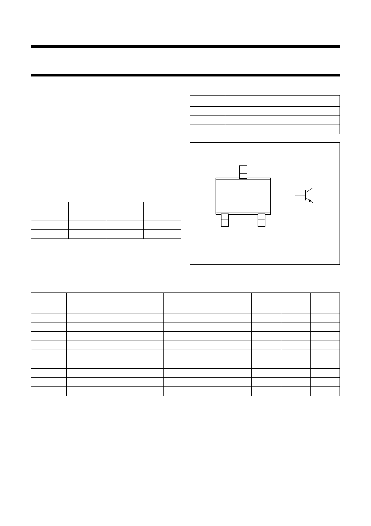
PINNING
PIN DESCRIPTION
1 base
2 emitter
3 collector
handbook, halfpage
Top view
3
1
1
2
MAM048
Fig.1 Simplified outline (SOT323) and symbol.
3
2
LIMITING VALUES
In accordance with the Absolute Maximum Rating System (IEC 134).
SYMBOL PARAMETER CONDITIONS MIN. MAX. UNIT
V
CBO
V
CEO
V
EBO
I
C
I
CM
I
BM
P
tot
T
stg
T
j
T
amb
collector-base voltage open emitter −−50 V
collector-emitter voltage open base; IC= −10 mA −−45 V
emitter-base voltage open collector −−5V
collector current (DC) −−500 mA
peak collector current −−1A
peak base current −−200 mA
total power dissipation T
≤ 25 °C; note 1 − 200 mW
amb
storage temperature −65 +150 °C
junction temperature − 150 °C
operating ambient temperature −65 +150 °C
Note
1. Transistor mounted on an FR4 printed-circuit board.
1999 May 18 2
Philips Semiconductors Product specification
PNP general purpose transistor BC807W
THERMAL CHARACTERISTICS
SYMBOL PARAMETER CONDITIONS VALUE UNIT
R
th j-a
Note
1. Transistor mounted on an FR4 printed-circuit board.
CHARACTERISTICS
=25°C unless otherwise specified.
T
amb
SYMBOL PARAMETER CONDITIONS MIN. MAX. UNIT
I
CBO
I
EBO
h
FE
V
CEsat
V
BE
C
c
f
T
thermal resistance from junction to ambient note 1 625 K/W
collector cut-off current IE= 0; VCB= −20 V −−100 nA
I
= 0; VCB= −20 V; Tj= 150 °C −−5µA
E
emitter cut-off current IC= 0; VEB= −5V −−100 nA
DC current gain IC= −100 mA; VCE= −1 V; note 1;
BC807W 100 600
see Figs 2, 3 and 4
BC807-16W 100 250
BC807-25W 160 400
BC807-40W 250 600
DC current gain I
collector-emitter saturation
= −500 mA; VCE= −1 V; note 1 40 −
C
IC= −500 mA; IB= −50 mA; note 1 −−700 mV
voltage
base-emitter voltage IC= −500 mA; VCE= −1 V; note 1 −−1.2 V
collector capacitance IE=ie= 0; VCB= −10 V; f = 1 MHz − 10 pF
transition frequency IC= −10 mA; VCE= −5 V; f = 100 MHz 80 − MHz
Note
1. Pulse test: t
≤ 300 µs; δ≤0.02.
p
1999 May 18 3
 Loading...