

Philips BB119 Datasheet
DISCRETE SEMICONDUCTORS
DATA SH EET
M3D176
BB119
Variable capacitance diode
Product specification
Supersedes data of April 1992
File under Discrete Semiconductors, SC01
1996 May 03
Philips Semiconductors Product specification
Variable capacitance diode BB119
FEATURES
• Hermetically sealed leaded glass
SOD27 (DO-35) package
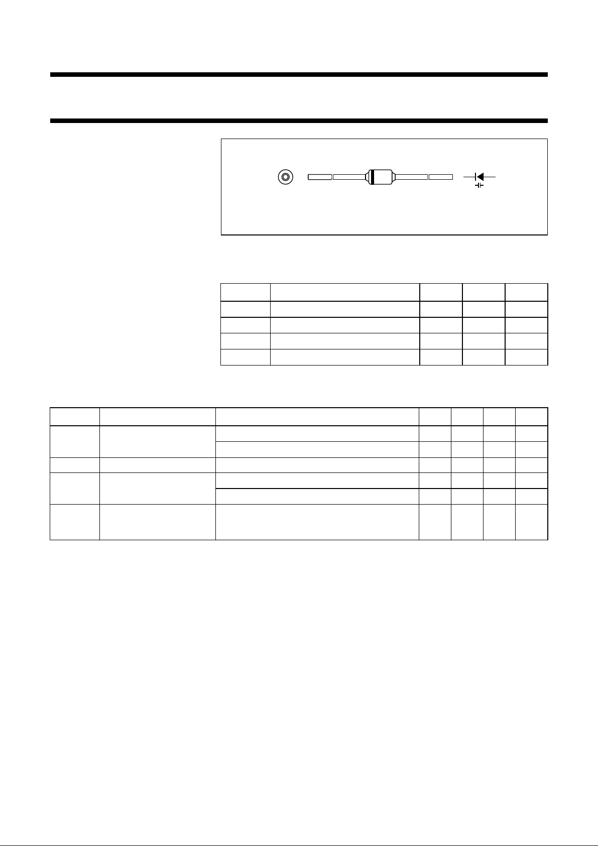
handbook, halfpage
k
a
• C10: 17 pF; ratio: 1.3.
MAM238
APPLICATIONS
Fig.1 Simplified outline (SOD27; DO-35) and symbol.
• Automatic frequency control.
DESCRIPTION
The BB119 is a variable capacitance
diode, fabricated in planar
technology, and encapsulated in the
hermetically sealed leaded glass
SOD27 (DO-35) package.
LIMITING VALUES
In accordance with the Absolute Maximum Rating System (IEC 134).
SYMBOL PARAMETER MIN. MAX. UNIT
V
R
I
F
T
stg
T
j
continuous reverse voltage
continuous forward current −
storage temperature
operating junction temperature
−
−55
−
15 V
200 mA
+150 °C
150 °C
ELECTRICAL CHARACTERISTICS
T
=25°C; unless otherwise specified.
j
SYMBOL PARAMETER CONDITIONS MIN. TYP. MAX. UNIT
I
R
r
s
C
d
C
d4V()
-------------------C
d10V()
reverse current VR= 15 V; see Fig.3 −−
= 15 V; Tj= 150 °C; see Fig.3 −−
V
R
50
2
diode series resistance f = 200 MHz; note 1 − 0.2 1.5 Ω
diode capacitance VR= 4 V; f = 1 MHz; see Figs 2 and 4
= 10 V; f = 1 MHz; see Figs 2 and 4
V
R
20
− 17 − pF
−
25 pF
capacitance ratio f = 1 MHz 1.3 −−
nA
µA
Note
1. V
=4V.
R
1996 May 03 2
 Loading...