

Philips BAS70-07S Datasheet
DISCRETE SEMICONDUCTORS
DATA SH EET
alfpage
MBD128
BAS70-07S
Schottky barrier double diode
Product specification
Supersedes data of 1998 Feb 06
1998 Jul 10

Philips Semiconductors Product specification
Schottky barrier double diode BAS70-07S
FEATURES
• Low forward voltage
• Guard ring protected
• Small SMD package.
APPLICATIONS
• Ultra high-speed switching
• Voltage clamping
• Protection circuits
• Blocking diodes.
DESCRIPTION
Planar Schottky barrier double diode
with an integrated guard ring for
stress protection.
Two separate dies are encapsulated
in a SOT363 small SMD plastic
package.
PINNING
PIN DESCRIPTION
1 anode (a
)
1
2,5 not connected
3 cathode (k
4 anode (a
6 cathode (k
654
123
Top view
Marking code: 77.
)
2
)
2
)
1
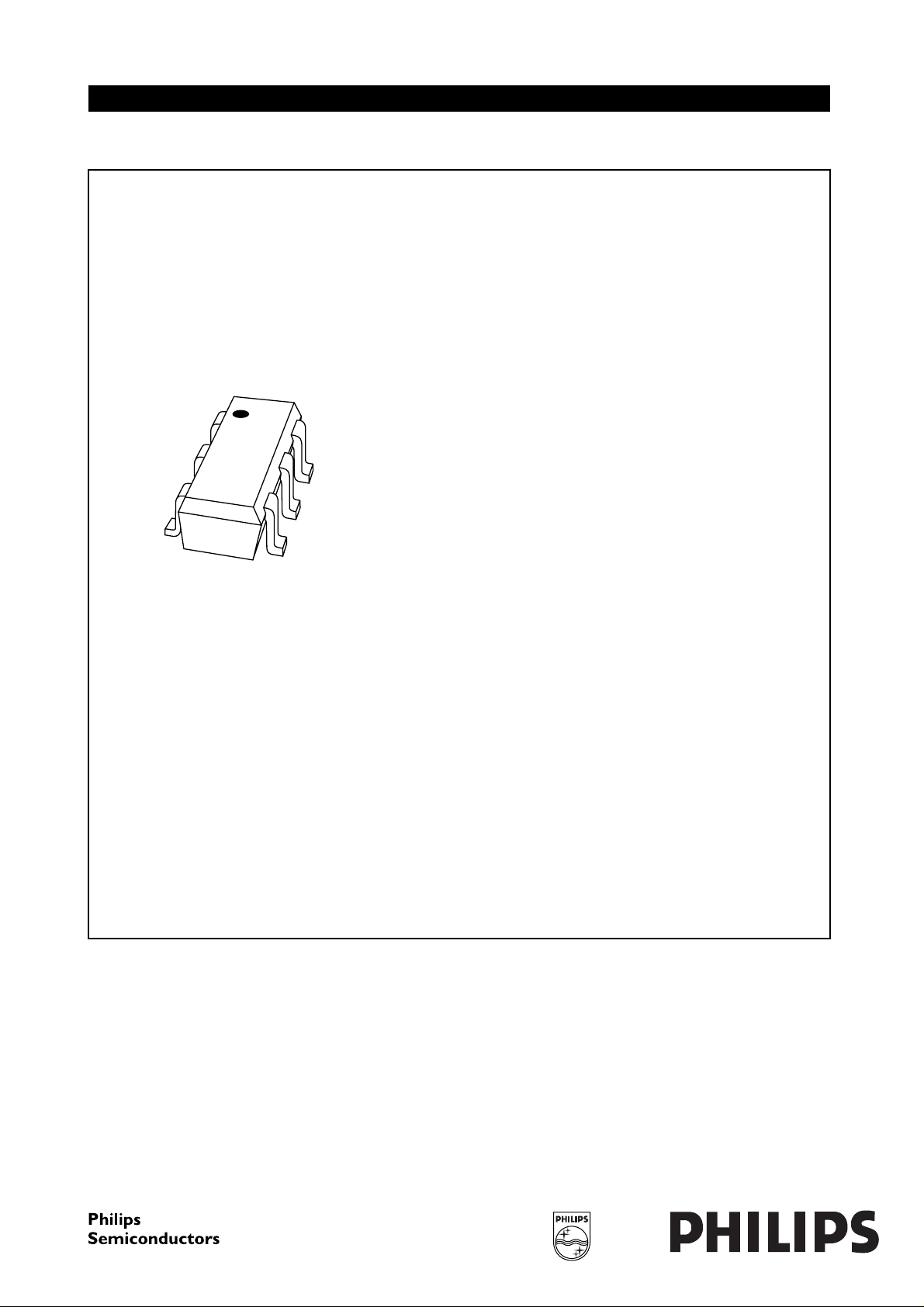
handbook, 2 columns
MSA370
Fig.1 Simplified outline (SOT363) and symbol.
14
63
MBK149
1998 Jul 10 2

Philips Semiconductors Product specification
Schottky barrier double diode BAS70-07S
LIMITING VALUES
In accordance with the Absolute Maximum Rating System (IEC 134).
SYMBOL PARAMETER CONDITIONS MIN. MAX. UNIT
Per diode
V
I
F
I
FRM
I
FSM
T
T
T
R
stg
j
amb
continuous reverse voltage
continuous forward current −
repetitive peak forward current tp≤ 1s;δ≤0.5
non-repetitive peak forward current tp< 10 ms
storage temperature
junction temperature
operating ambient temperature
ELECTRICAL CHARACTERISTICS
T
=25°C unless otherwise specified.
amb
−
−
−
−65
−
−65
70 V
70 mA
70 mA
100 mA
+150 °C
150 °C
+150 °C
SYMBOL PARAMETER CONDITIONS MAX. UNIT
Per diode
V
F
I
R
τ charge carrier life time (Krakauer
forward voltage see Fig.2
I
=1mA
F
=10mA
I
F
I
=15mA
F
reverse current VR= 50 V; note 1; see Fig.3
= 70 V; note 1; see Fig.3
V
R
=5mA
I
F
410 mV
750 mV
1V
100
10
nA
µA
100 ps
method)
C
d
diode capacitance f = 1 MHz; VR= 0; see Fig.5
2pF
Note
1. Pulsed test: t
= 300 µs; δ = 0.02.
p
THERMAL CHARACTERISTICS
SYMBOL PARAMETER CONDITIONS VALUE UNIT
R
th j-a
thermal resistance from junction to ambient note 1 416 K/W
Note
1. Refer to SOT363 standard mounting conditions.
1998 Jul 10 3
 Loading...