

Philips BAS70-05, BAS70-04, BAS70-07 Datasheet
DISCRETE SEMICONDUCTORS
DATA SH EET
ge
M3D088
M3D071
BAS70 series
Schottky barrier (double) diodes
Product specification
Supersedes data of 1996 Oct 01
1999 Jun 01
Philips Semiconductors Product specification
Schottky barrier (double) diodes BAS70 series
FEATURES
• Low forward current
• High breakdown voltage
• Guard ring protected
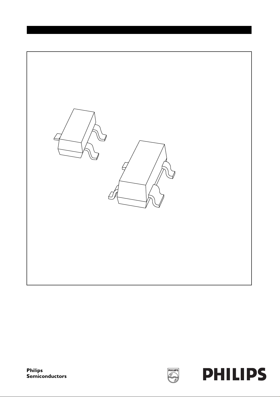
• Small plastic SMD package
• Low diode capacitance.
APPLICATIONS
• Ultra high-speed switching
• Voltage clamping
• Protection circuits.
DESCRIPTION
Planar Schottky barrier diodes with an
integrated guard ring for stress
protection. Single diodes and double
diodes with different pinning are
available.
The diodes BAS70, BAS70-04,
BAS70-05 and BAS70-06 are
encapsulated in a SOT23 small
plastic SMD package. The BAS70-07
is encapsulated in a SOT143B small
plastic SMD package.
MARKING
TYPE NUMBER
MARKING
(1)
CODE
BAS70 73p∗
BAS70-04 74p∗
BAS70-05 75p∗
BAS70-06 76p∗
BAS70-07 77p
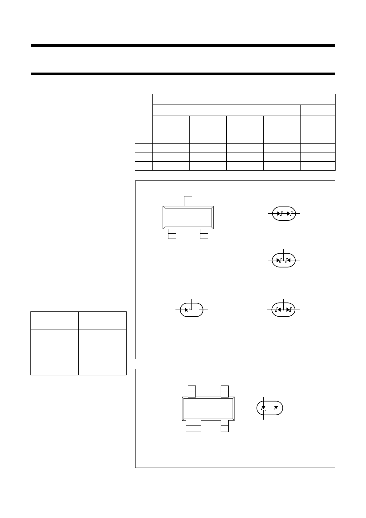
PINNING
DESCRIPTION
PIN
BAS70
(see Fig.1b)
1a
1
BAS70-04
(see Fig.1c)
2 n.c. k
3k
1
4 −−−−a
handbook, 2 columns
Top view
3
a. Simplified outline SOT23.
SOT23 SOT143B
a
1
2
k
1,a2
21
MGC482
BAS70-05
(see Fig.1d)
a
1
a
2
k1,k
2
handbook, 2 columns
handbook, 2 columns
BAS70-06
(see Fig.1e)
k
1
k
2
a1,a
2
3
12
MGC485
c. BAS70-04
3
12
MGC484
BAS70-07
(see Fig.2)
k
1
k
2
a
2
1
d. BAS70-05.
handbook, 2 columns
1
3
2
n.c.
MGC483
handbook, 2 columns
3
12
MGC486
e. BAS70-06.b. BAS70 single diode.
Fig.1 Simplified outline (SOT23) and symbols.
Note
1. ∗ = -: Made in Hong Kong.
handbook, halfpage
∗ = t: Made in Malaysia.
Fig.2 Simplified outline (SOT143B) BAS70-07 and symbol.
1999 Jun 01 2
43
Top view
21
4
1
MAM194
3
2
Philips Semiconductors Product specification
Schottky barrier (double) diodes BAS70 series
LIMITING VALUES
In accordance with the Absolute Maximum Rating System (IEC 134).
SYMBOL PARAMETER CONDITIONS MIN. MAX. UNIT
Per diode
V
I
F
I
FRM
I
FSM
T
T
T
R
stg
j
amb
continuous reverse voltage
continuous forward current −
repetitive peak forward current tp≤ 1s;δ≤0.5
non-repetitive peak forward current tp< 10 ms
storage temperature
junction temperature
operating ambient temperature
ELECTRICAL CHARACTERISTICS
T
=25°C unless otherwise specified.
amb
−
−
−
−65
−
−65
70 V
70 mA
70 mA
100 mA
+150 °C
150 °C
+150 °C
SYMBOL PARAMETER CONDITIONS MAX. UNIT
Per diode
V
F
I
R
τ charge carrier life time (Krakauer
forward voltage see Fig.3
I
=1mA
F
=10mA
I
F
I
=15mA
F
reverse current VR= 50 V; note 1; see Fig.4
= 70 V; note 1; see Fig.4
V
R
=5mA
I
F
410 mV
750 mV
1V
100
10
nA
µA
100 ps
method)
C
d
diode capacitance f = 1 MHz; VR= 0; see Fig.6
2pF
Note
1. Pulse test: t
= 300 µs; δ = 0.02.
p
THERMAL CHARACTERISTICS
SYMBOL PARAMETER CONDITIONS VALUE UNIT
R
th j-a
thermal resistance from junction to ambient note 1 500 K/W
Note
1. Refer to SOT23 or SOT143B standard mounting conditions.
1999 Jun 01 3
 Loading...