

Philips NE5517, NE5517A, AU5517 Operation Manual

查询AU5517D供应商查询AU5517D供应商
INTEGRATED CIRCUITS
NE5517/NE5517A/AU5517
Dual operational transconductance
amplifier
Product data
Replaces NE5517/NE5517A dated 2001 Aug 03
2002 Dec 06
Philips Semiconductor Product data
Dual operational transconductance amplifier
DESCRIPTION
The AU5517 and NE5517 contain two current-controlled
transconductance amplifiers, each with a differential input and
push-pull output. The AU5517/NE5517 offers significant design and
performance advantages over similar devices for all types of
programmable gain applications. Circuit performance is enhanced
through the use of linearizing diodes at the inputs which enable a
10 dB signal-to-noise improvement referenced to 0.5% THD. The
AU5517/NE5517 is suited for a wide variety of industrial and
consumer applications.
Constant impedance buffers on the chip allow general use of the
AU5517/NE5517. These buffers are made of Darlington transistors
and a biasing network that virtually eliminate the change of offset
voltage due to a burst in the bias current I
, hence eliminating the
ABC
audible noise that could otherwise be heard in high quality audio
applications.
FEA TURES
•Constant impedance buffers
•∆V
of buffer is constant with amplifier I
BE
BIAS
change
•Excellent matching between amplifiers
•Linearizing diodes
•High output signal-to-noise ratio
APPLICA TIONS
•Multiplexers
•Timers
•Electronic music synthesizers
•Dolby HX Systems
•Current-controlled amplifiers, filters
•Current-controlled oscillators, impedances
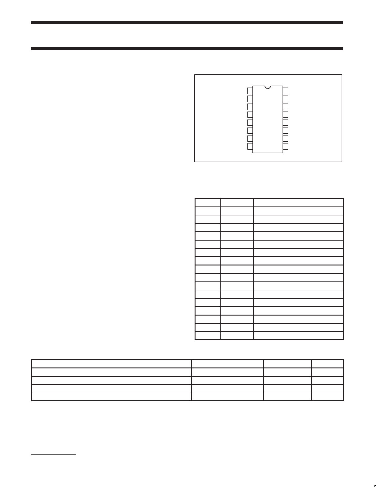
PIN CONFIGURATION
PIN DESIGNA TION
PIN NO. SYMBOL NAME AND FUNCTION
NE5517/NE5517A/
N, D Packages
1
I
ABCa
2
D
a
3
+IN
a
4
–IN
a
5
VO
a
6
V–
INBUFFER
VO
BUFFERa
1 I
2 D
3 +IN
4 –IN
5 V
6 V– Negative supply
7 IN
BUFFERa
8 VO
9 VO
10 IN
BUFFERb
11 V+ Positive supply
12 V
13 –IN
14 +IN
15 D
16 I
7
a
8
Top View
Figure 1. Pin Configuration
ABCa
Oa
Amplifier bias input A
Diode bias A
a
Non-inverting input A
a
Inverting input A
a
Output A
Buffer input A
BUFFERa
BUFFERb
Buffer output A
Buffer output B
Buffer input B
Ob
ABCb
Output B
Inverting input B
b
Non-inverting input B
b
Diode bias B
b
Amplifier bias input B
16
15
14
13
12
11
10
9
I
ABCb
D
b
+IN
b
–IN
b
VO
b
V+
IN
BUFFERb
VO
BUFFERb
SL00306
AU5517
ORDERING INFORMATION
DESCRIPTION TEMPERATURE RANGE ORDER CODE DWG #
16-Pin Plastic Dual In-Line Package (DIP) 0 to +70 °C NE5517N SOT38-4
16-Pin Plastic Dual In-Line Package (DIP) 0 to +70 °C NE5517AN SOT38-4
16-Pin Small Outline (SO) Package 0 to +70 °C NE5517D SOT109-1
16-Pin Small Outline (SO) Package –40 to +125 °C AU5517D SOT109-1
Dolby is a registered trademark of Dolby Laboratories Inc., San Francisco, Calif.
2002 Dec 06
2
Philips Semiconductor Product data
Dual operational transconductance amplifier
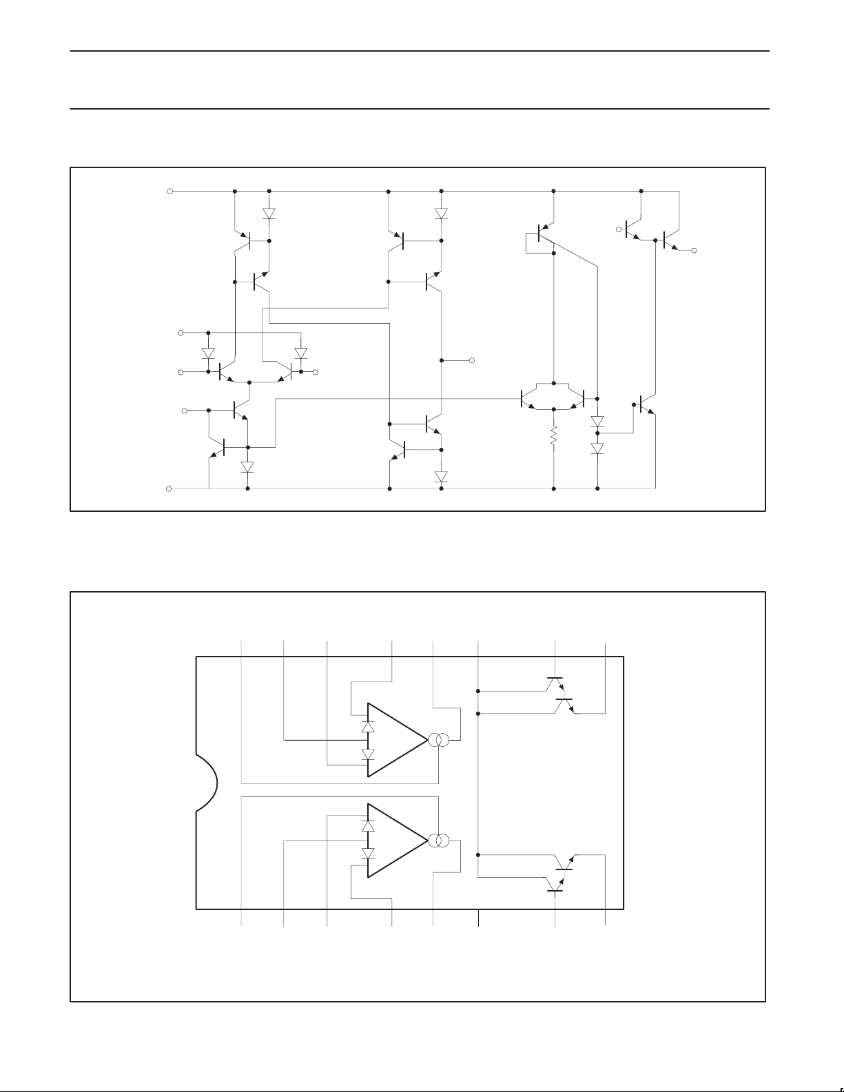
CIRCUIT SCHEMATIC
V+
11
D4
2,15
–INPUT
AMP BIAS
INPUT
V–
6
4,13
1,16
Q6
Q7
D2
Q4
Q5
Q2
Q1
D1
D3
+INPUT
3,14
Q10
Q8
Figure 2. Circuit Schematic
Q9
Q11
NE5517/NE5517A/
AU5517
D6
Q14
V
OUTPUT
5,12
Q15 Q16
R1
D5
7,10
D7
D8
Q12
Q13
8,9
Q3
SL00307
CONNECTION DIAGRAM
B
AMP
BIAS
INPUT
16 15 14 13 12 11 10 9
INPUT
NOTE:
1. V+ of output buffers and amplifiers are internally connected.
DIODE
123 45 6 7 8
AMP
DIODE
BIAS
A
B
BIAS
BIAS
AA
B
INPUT
(+)
INPUT
(+)
Figure 3. Connection Diagram
INPUT
–
+
+
–
INPUT
B
(–)
(–)
A
B
OUTPUT
B
A
OUTPUT
V+ (1)
A
V–
B
BUFFER
INPUT
BUFFER
INPUT
A
B
BUFFER
OUTPUT
BUFFER
OUTPUT
A
SL00308
2002 Dec 06
3
Philips Semiconductor Product data
Dual operational transconductance amplifier
NE5517/NE5517A/
AU5517
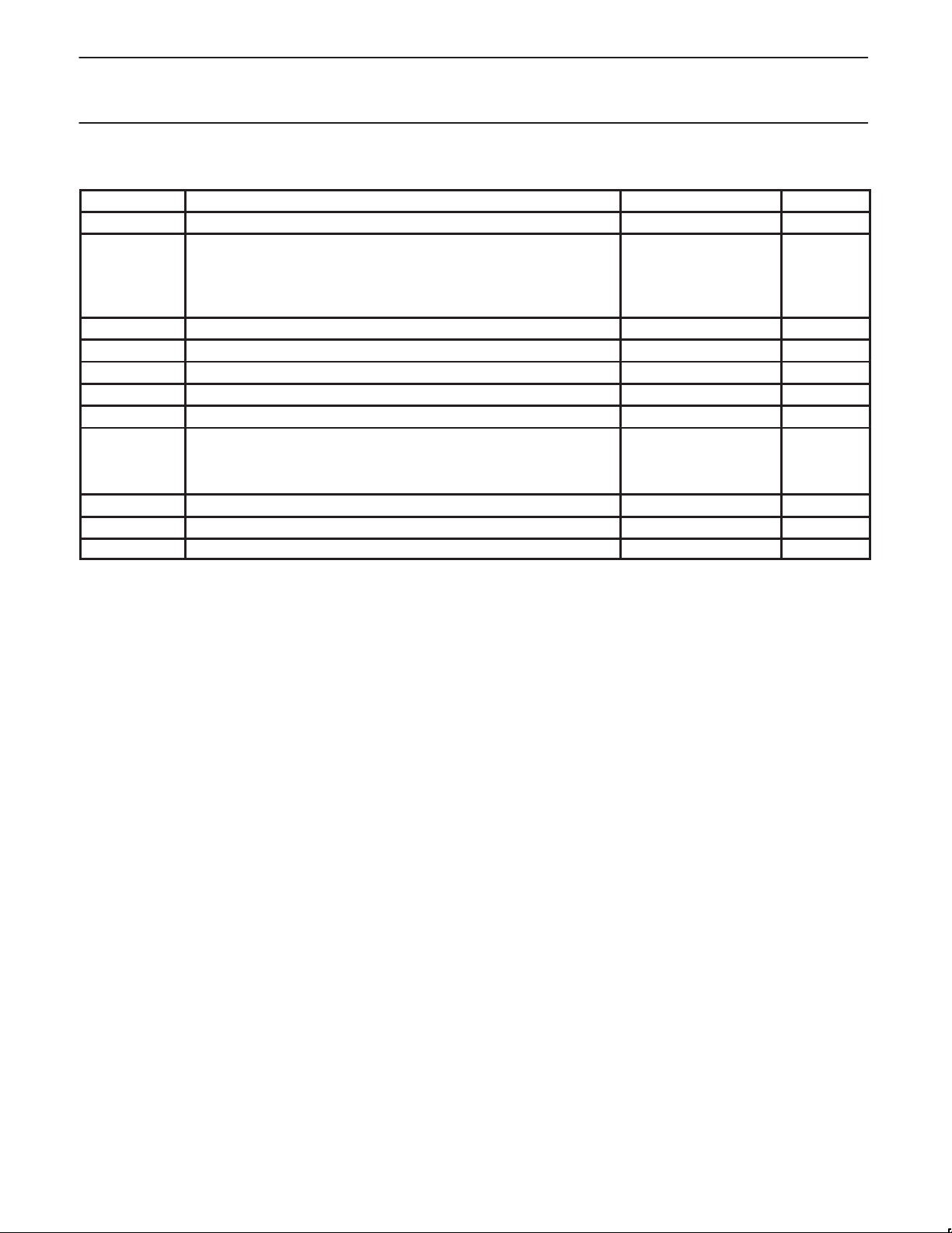
ABSOLUTE MAXIMUM RATINGS
SYMBOL PARAMETER RATING UNIT
V
S
P
D
Supply voltage
Power dissipation,
T
= 25 °C (still air)
amb
NE5517N, NE5517AN 1500 mW
NE5517D, AU5517D 1125 mW
V
I
D
I
ABC
I
SC
I
OUT
T
IN
amb
Differential input voltage ±5 V
Diode bias current 2 mA
Amplifier bias current 2 mA
Output short-circuit duration Indefinite
Buffer output current
Operating temperature range
NE5517N, NE5517AN 0 °C to +70 °C °C
AU5517D –40 °C to +125 °C °C
V
DC
T
stg
T
sld
DC input voltage +VS to –V
Storage temperature range –65 °C to +150 °C °C
Lead soldering temperature (10 sec max) 230 °C
NOTES:
1. For selections to a supply voltage above ±22 V, contact factory
2. The following derating factors should be applied above 25 °C
N package at 12.0 mW/°C
D package at 9.0 mW/°C
3. Buffer output current should be limited so as to not exceed package dissipation.
1
2
3
44 VDC or ±22 V
20 mA
S
2002 Dec 06
4
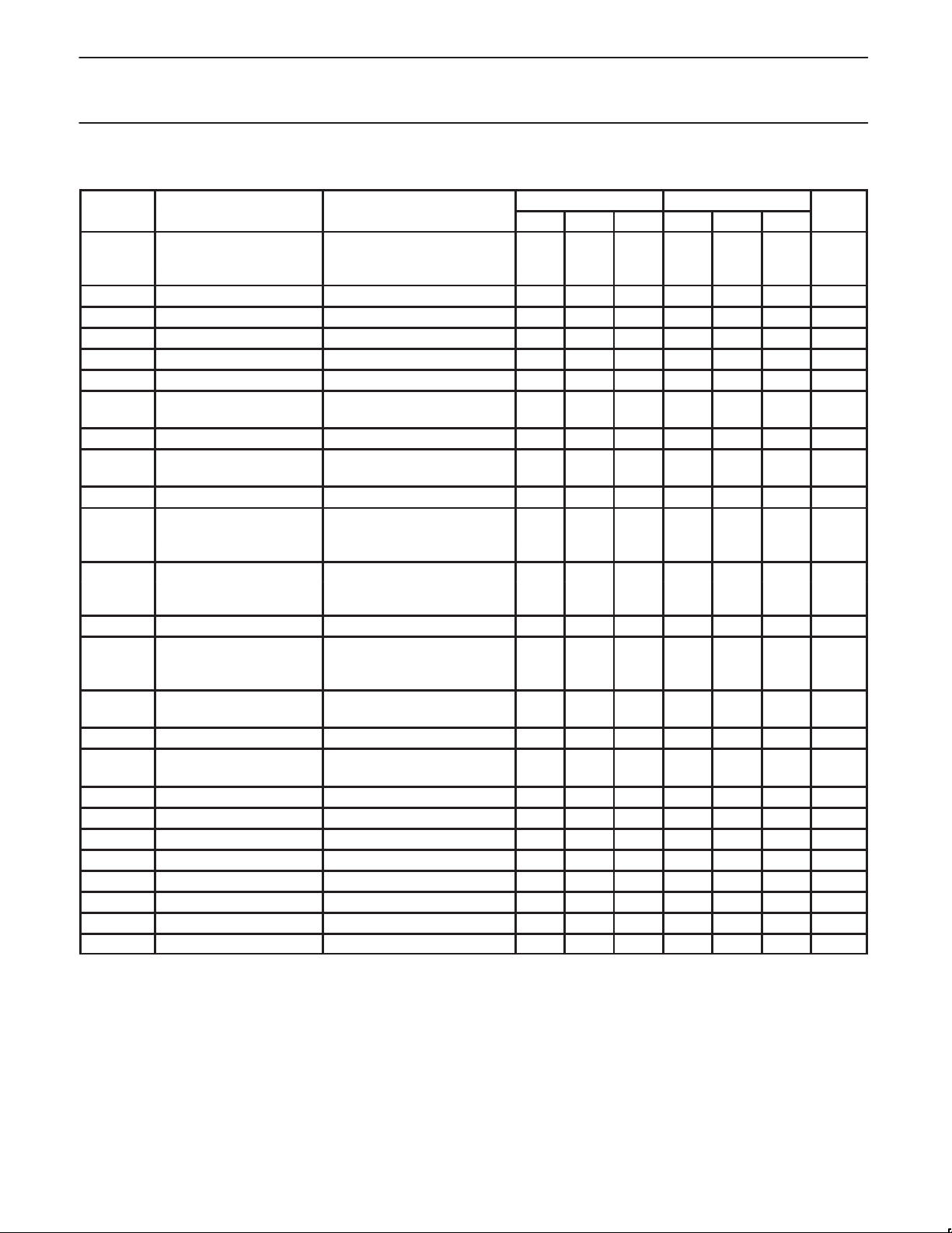
Philips Semiconductor Product data
SYMBOL
PARAMETER
TEST CONDITIONS
UNIT
I
BIAS
In ut bias current
gMForward transconductance
Dual operational transconductance amplifier
NE5517/NE5517A/
AU5517
DC ELECTRICAL CHARACTERISTICS
V
OS
V
OS
I
OS
I
OUT
V
OUT
I
CC
CMRR
I
IN
R
IN
B
W
SR Slew rate Unity gain compensated 50 50 V/µs
IN
BUFFER
VO
BUFFER
NOTES:
1. These specifications apply for V
specified. The inputs to the buffers are grounded and outputs are open.
2. These specifications apply for V
connected to the transconductance amplifier output.
= ±15, R
3. V
S
Input offset voltage Over temperature range 5 mV
∆VOS/∆T Avg. TC of input offset voltage 7 7 µV/°C
VOS including diodes Diode bias current (ID) = 500 µA 0.5 5 0.5 2 mV
Input offset change 5 µA ≤ I
Input offset current 0.1 0.6 0.1 0.6 µA
∆IOS/∆T Avg. TC of input offset current 0.001 0.001 µA/°C
p
∆IB/∆T Avg. TC of input current 0.01 0.01 µA/°C
gM tracking 0.3 0.3 dB
Peak output current RL = 0, I
Peak output voltage
Positive RL = ∞, 5 µA ≤ I
Negative RL = ∞, 5 µA ≤ I
Supply current I
VOS sensitivity
Positive ∆ VOS/∆ V+ 20 150 20 150 µV/V
Negative ∆ VOS/∆ V– 20 150 20 150 µV/V
Common-mode rejection
ration
Common-mode range ±12 ±13.5 ±12 ±13.5 V
Crosstalk
Differential input current I
Leakage current I
Input resistance 10 26 10 26 kΩ
Open-loop bandwidth 2 2 MHz
Buffer input current 5 0.4 5 0.4 5 µA
Peak buffer output voltage 5 10 10 V
∆VBE of buffer Refer to Buffer VBE test circuit
= ±15 V, T
S
= ±15 V, I
S
= 5 kΩ connected from Buffer output to –VS and 5 µA ≤ I
OUT
1
AU5517/NE5517 NE5517A
Min Typ Max Min Typ Max
0.4 5 0.4 2 mV
I
5 µA 0.3 5 0.3 2 mV
ABC
≤ 500 µA 0.1 0.1 3 mV
ABC
0.4 5 0.4 5 µA
Over temperature range 1 8 1 7 µA
6700 9600 1300 7700 9600 1200 µmho
Over temperature range 5400 4000 µmho
RL = 0, I
=5 µA 5 3 5 7 µA
ABC
= 500 µA 350 500 650 350 500 650 µA
ABC
RL = 0 300 300 µA
≤ 500 µA +12 +14.2 +12 +14.2 V
ABC
≤ 500 µA –12 –14.4 –12 –14.4 V
ABC
= 500 µA, both channels 2.6 4 2.6 4 mA
ABC
80 110 80 110 dB
Referred to input2
20 Hz < f < 20 kHz
= 0, input = ±4 V 0.02 100 0.02 10 nA
ABC
= 0 (Refer to test circuit) 0.2 100 0.2 5 nA
ABC
3
= 25 °C, amplifier bias current (I
amb
= 500 µA, R
ABC
= 5 kΩ connected from the buffer output to –VS and the input of the buffer is
OUT
≤ 500 µA.
ABC
100 100 dB
0.5 5 0.5 5 mV
) = 500 µA, Pins 2 and 15 open unless otherwise
ABC
2002 Dec 06
5
Philips Semiconductor Product data
Dual operational transconductance amplifier
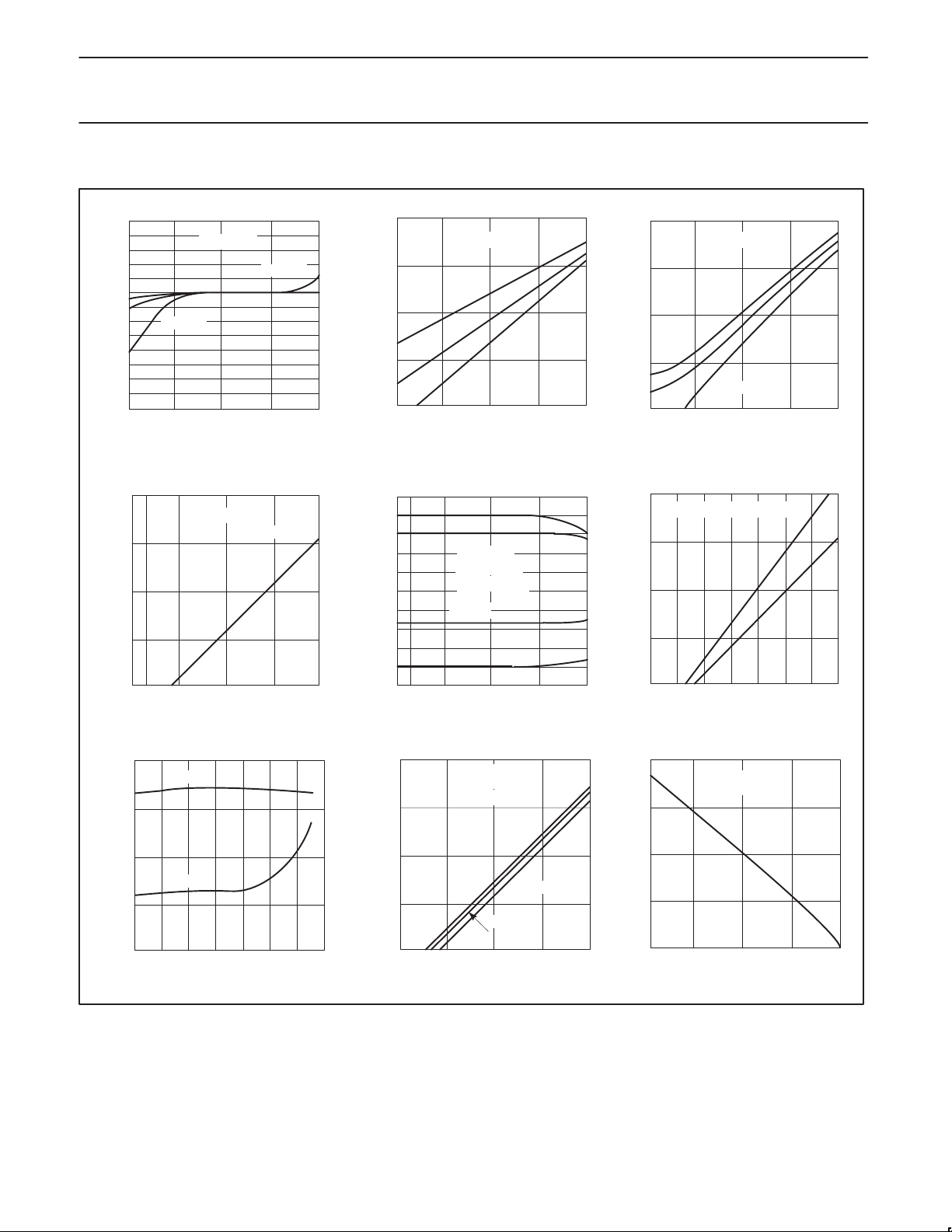
TYPICAL PERFORMANCE CHARACTERISTICS
Input Offset Voltage
VS = ±15V
-55°C
+25°C
+125°C
0.1µA1µA10µA 100µA 1000µA
AMPLIFIER BIAS CURRENT (I
Peak Output Current
VS = ±15V
0.1µA1µA10µA 100µA 1000µA
AMPLIFIER BIAS CURRENT (I
INPUT OFFSET VOLTAGE (mV)
µ
PEAK OUTPUT CURRENT ( A)
5
4
3
2
1
0
-1
-2
-3
-4
-5
-6
-7
-8
4
10
3
10
2
10
10
1
+125°C
ABC
+125°C
ABC
)
+25°C
-55°C
3
10
2
10
10
1
INPUT OFFSET CURRENT (nA)
0.1
5
4
3
2
1
0
-1
-2
-3
-4
-5
COMMON-MODE RANGE (V)
-6
PEAK OUTPUT VOLTAGE AND
-7
-8
)
Input Bias Current
VS = ±15V
-55°C
+25°C
0.1µA1µA10µA 100µA 1000µA
AMPLIFIER BIAS CURRENT (I
Peak Output Voltage and
Common-Mode Range
V
OUT
V
CMR
VS = ±15V
RLOAD = ∞
T
amb
V
CMR
V
OUT
0.1µA1µA10µA 100µA 1000µA
AMPLIFIER BIAS CURRENT (I
+125°C
= 25°C
ABC
ABC
NE5517/NE5517A/
AU5517
4
10
3
10
2
10
10
INPUT BIAS CURRENT (nA)
1
)
5
10
4
10
3
10
2
10
LEAKAGE CURRENT (pA)
10
-50°C -25°C0°C25°C50°C75°C100°C125°C
)
Input Bias Current
VS = ±15V
-55°C
+25°C
0.1µA1µA10µA 100µA 1000µA
AMPLIFIER BIAS CURRENT (I
+125°C
ABC
)
Leakage Current
(+)VIN = (–)VIN = V
AMBIENT TEMPERATURE (TA)
OUT
= 36V
0V
4
10
3
10
2
10
10
INPUT LEAKAGE CURRENT (pA)
1
012345 67
Input Leakage
+125°C
+25°C
INPUT DIFFERENTIAL VOLTAGE
2002 Dec 06
5
10
µ
4
10
3
10
2
10
TRANSCONDUCTANCE (gM) — ( ohm)
10
Transconductance
gM
0.1µA1µA10µA 100µA 1000µA
AMPLIFIER BIAS CURRENT (I
PINS 2, 15
VS = ±15V
-55°C
OPEN
+25°C
+125°C
ABC
)
mq
m
M
Figure 4. Typical Performance Characteristics
6
2
10
Ω
1
10
1
0.1
INPUT RESISTANCE (MEG )
0.01
Input Resistance
PINS 2, 15
OPEN
0.1µA1µA10µA 100µA 1000µA
AMPLIFIER BIAS CURRENT (I
ABC
SL00309
)
 Loading...