

Philips AU2902N, AU2902D Datasheet
Philips Semiconductors Linear Products Product specification
AU2902Low power quad operational amplifier
42
August 31, 1994 853-1634 13721
DESCRIPTION
The AU2902 consists of four independent, high-gain, internally
frequency-compensated operational amplifiers designed specifically
to operate from a single power supply over a wide range of voltages.
UNIQUE FEATURES
In the linear mode, the input common-mode voltage range includes
ground and the output voltage can also swing to ground, even
though operated from only a single power supply voltage.
The unity gain crossover frequency and the input bias current are
temperature-compensated.
FEATURES
•Internally frequency-compensated for unity gain
•Large DC voltage gain: 100dB
•Wide bandwidth (unity gain): 1MHz (temperature-compensated)
•Wide power supply range Single supply: 3V
DC
to 30VDC or dual
supplies: ±1.5V
DC
to ±15V
DC
•Very low supply current drain: essentially independent of supply
voltage (1mW/op amp at +5V
DC
)
•Low input bias current: 45nA
DC
(temperature-compensated)
•Low input offset voltage: 2mV
DC
and offset current: 5nA
DC
•Differential input voltage range equal to the power supply voltage
•Large output voltage: 0V
DC
to VCC-1.5VDC swing
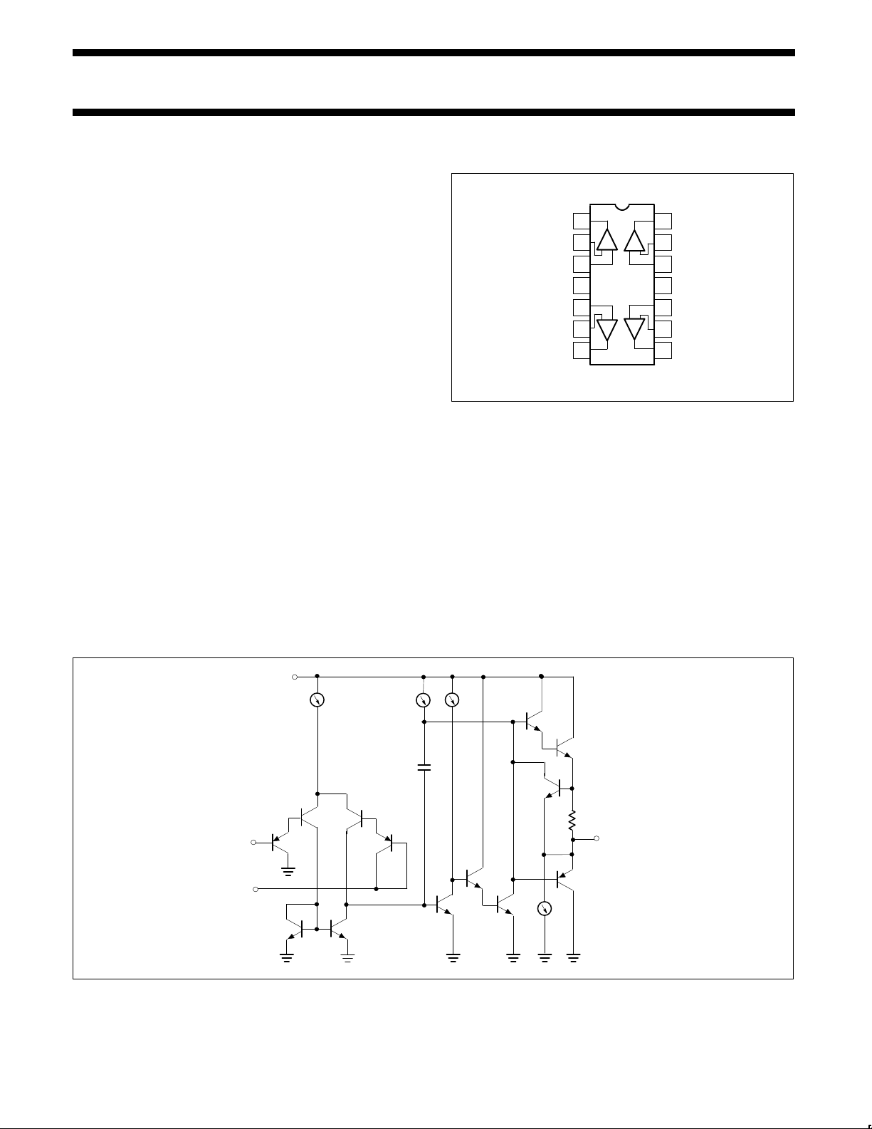
PIN CONFIGURATION
+
D and N Packages
1
2
3
4 11
12
13
14
OUTPUT 1
–INPUT 1
+INPUT 1
V+
1
–
4
+ –
+
7
6
5 10
9
8
2
–
3
+
–
OUTPUT 2
+INPUT 2
–INPUT 2
OUTPUT 4
–INPUT 4
+INPUT 4
GND
OUTPUT 3
+INPUT 3
–INPUT 3
Top View
EQUIVALENT SCHEMATIC
V–
OUTPUT
Q5
R
SC
Q8 Q9
Q1
Q3
6µA
100µA 6µA
Q6
Q7
Q13
Q12Q10
Q2
INPUT
50µA
C
C
Philips Semiconductors Linear Products Product specification
AU2902Low power quad operational amplifier
August 31, 1994
43
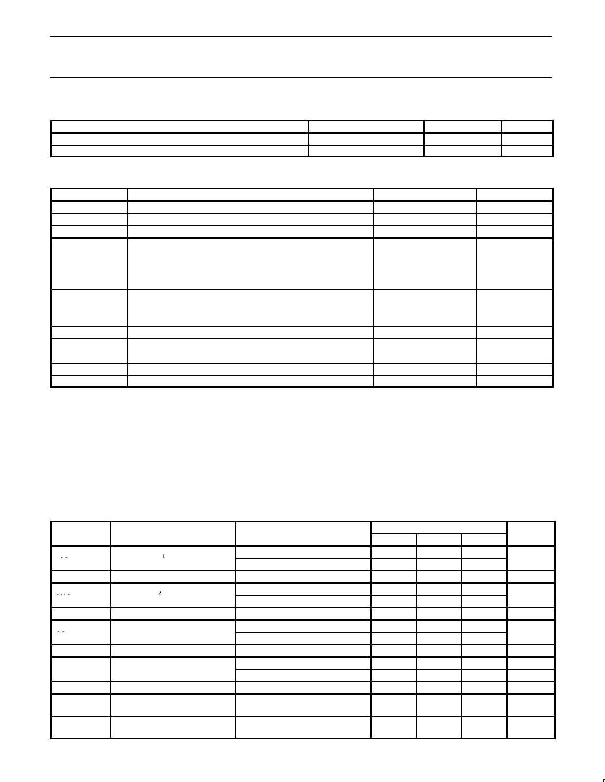
ORDERING INFORMATION
DESCRIPTION TEMPERATURE RANGE ORDER CODE DWG #
14-Pin Plastic Dual In-Line Package (DIP) -40 to +125°C AU2902N 0405B
14-Pin Plastic Small Outline (SO) Package -40 to +125°C AU2902D 0175D
ABSOLUTE MAXIMUM RATINGS
SYMBOL PARAMETER RATING UNIT
V
CC
Supply voltage 32 or ±16 V
DC
V
IN
Differential input voltage 32 V
DC
V
IN
Input voltage –0.3 to +32 V
DC
P
DMAX
Maximum power dissipation,
TA=25°C(still–air)
1
N package 1420 mW
D package 1040 mW
Output short–circuit to GND one
amplifier Continuous
VCC<15VDC and TA=25°C
I
IN
Input current (VIN<–0.3V)
3
50 mA
T
A
Operating ambient temperature range
AU2902 –40 to +125 °C
T
STG
Storage temperature range –65 to +150 °C
T
SOLD
Lead soldering temperature (10sec max) 300 °C
NOTES:
1. Derate above 25°C at the following rates:
N package at 11.4mW/°C
D package at 8.3mW/°C
2. Short–circuits from the output to V
CC
+ can cause excessive heating and eventual destruction. The maximum output current is approximately
40mA, independent of the magnitude of V
CC
. At values of supply voltage in excess of +15VDC continuous short–circuits can exceed the
power dissipation ratings and cause eventual destruction.
3. This input current will only exist when the voltage at any of the input leads is driven negative. It is due to the collector–base junction of the
input PNP transistors becoming forward biased and thereby acting as input bias clamps. In addition, there is also lateral NPN parasitic transistor action on the IC chip. This action can cause the output voltages of the op amps to go to the V+ rail (or to ground for a large overdrive)
during the time that the input is driven negative.
DC ELECTRICAL CHARACTERISTICS
VCC=5V, TA=25°C unless otherwise specified.
AU2902
SYMBOL
PARAMETER
TEST CONDITIONS
Min Typ Max
UNIT
RS=0Ω ±2 ±7
VOSOffset voltage
1
RS=0Ω, over temp. ±9
mV
∆VOS/∆T Temperature drift RS=0Ω, over temp. 7 µV/°C
IIN(+) or IIN(–) 45 250
I
BIAS
Input current
2
IIN(+) or IIN(–), over temp. 40 500
nA
∆I
BIAS
/∆T Temperature drift Over temp. 50 pA/°C
IIN(+)–IIN(–) ±5 ±50
IOSOffset current
IIN(+)–IIN(–), over temp. ±150
nA
∆IOS/∆T Temperature drift Over temp. 10 pA/°C
V
CM
Common–mode voltage range
3
VCC≤30V 0 VCC–1.5 V
VCC≤30V, over temp. 0 VCC–2 V
CMRR Common–mode rejection ratio VCC=30V 65 70 dB
V
OUT
Output voltage swing
RL=2kΩ, VCC=30V,
over temp.
26 V
V
OH
Output voltage high
RL≥10kΩ, VCC=30V,
over temp.
27 28 V
 Loading...