

Philips ABT22V10A7A, ABT22V10A5A, ABT22V10A-BLA Datasheet

ABT22V10A5, A7
5V high-speed universal PLD device
with live insertion capability
Product specification 1996 Dec 16
INTEGRATED CIRCUITS
IC13 Data Handbook
Philips Semiconductors
Product specification
ABT22V10A5, A7
5V high-speed universal PLD device
with live insertion capability
2
1996 Dec 16 853–1795 17606
DESCRIPTION
The ABT22V10A is a versatile PAL device fabricated on Philips
BiCMOS process known as QUBiC.
The QUBiC process produces very high speed, 5 volt devices
(5.0ns) which have excellent noise immunity. The ground bounce of
an output held low while the 9 remaining outputs are switching is
less than 1.0V (typical).
The ABT22V10A outputs are designed to support Live
Insertion/Extraction into powered-up systems. The output is
specially designed so that during V
CC
ramp, the output remains
3-Stated until V
CC
≈ 2.1V. At that time, the outputs become fully
functional, depending upon device inputs. (See DC Electrical
Characteristics, Symbol I
PU/PD
, Page 4).
The ABT family of devices have virtually no ground bounce— less
than 1.0 volts V
OLP
, measured on an unswitched output (9 remaining
outputs switching, each with a 50pF load tied to ground).
The ABT family of devices has been designed with high drive
outputs (48mA sink and 16mA source currents), which allow for
direct connection to a backplane bus. This feature eliminates the
need for additional, standalone bus drivers, which are traditionally
required to boost the drive of a standard 16/–4mA PLDs.
Philips has developed a new means of testing the integrity of fuses,
both blown and intact fuses, which insures that all the fuses have
been correctly programmed and that each and every fuse—whether
“blown” or “intact”—is at the appropriate and optimal fuse resistance.
This dual verify scheme represents a significant improvement over
single reference voltage comparison schemes that have been used
for bipolar devices since the late 1980’s.
The ABT22V10A uses the familiar AND/OR logic array structure,
which allows direct implementation of sum-of-products equations.
This device has a programmable AND array, which drives a fixed
OR array. The OR sum-of-products feeds an “Output Macro Cell”
(OMC) that can be individually configured as a dedicated input, a
combinatorial output, or a registered output with internal feedback.
FEATURES
•Fastest 5V 22V10
•Low ground bounce (<1.0V typical)
•Live insertion/extraction permitted
•High output drive capability: 48mA/–16mA
•Varied product term distribution with up to 16 product terms per
output for complex functions
•Metastable hardened flip-flops
•Programmable output polarity
•Design support provided for third party CAD development and
programming hardware
•Improved fuse verification circuitry increases reliability
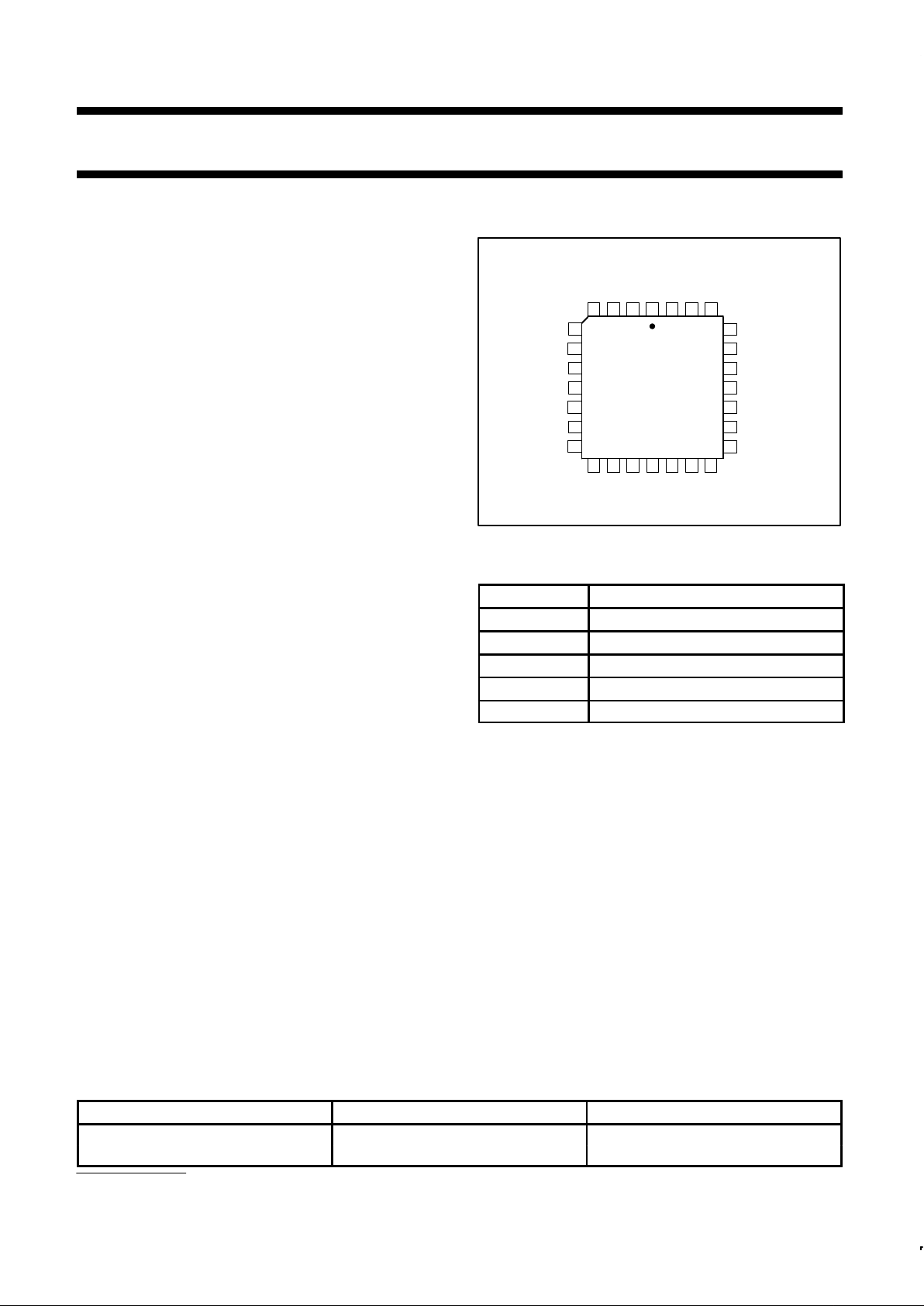
PIN CONFIGURATIONS
V
CC
1234
5
6
7
8
9
10
11
12 13 14 15 16 17 18
19
20
21
22
23
24
25
262728
GND
A Package
GND
I7
CLK/
I0
I1I2
I3
I4
I5
GND
I6
I8
I9 I10
GND
I11 F0 F1
F2
F3
F7
F6
F5
F4
F8F9
A = Plastic Leaded Chip Carrier
V
CC
SP00367
PIN LABEL DESCRIPTIONS
SYMBOL FUNCTION
I1 – I11 Dedicated Input
F0 – F9 Macro Cell Input/Output
CLK/I0 Clock Input/Dedicated Input
V
CC
Supply Voltage
GND Ground
ORDERING INFORMATION
DESCRIPTION ORDER CODE DRAWING NUMBER
ABT22V10A5A (5ns device)
28-Pin Plastic Leaded Chip Carrier
ABT22V10A7A (7.5ns device)
SOT261-3
PAL is a registered trademark of Advanced Micro Devices, Inc.
Philips Semiconductors Product specification
ABT22V10A5, A7
5V high-speed universal PLD device
with live insertion capability
1996 Dec 16
3
ABSOLUTE MAXIMUM RATINGS
1
RATINGS
SYMBOL
PARAMETER
MIN MAX
UNIT
V
CC
Supply voltage
2
–0.5 +7.0 V
DC
V
IN
Input voltage
2
–1.2 VCC + 0.5 V
DC
V
OUT
Output voltage –0.5 VCC + 0.5 V
DC
I
IN
Input currents –30 +30 mA
I
OUT
Output currents +100 mA
T
stg
Storage temperature range –65 +150 °C
NOTES:
1. Stresses above those listed may cause malfunction or permanent damage to the device. This is a stress rating only. Functional operation at
these or any other condition above those indicated in the operational and programming specification of the device is not implied.
2. Except in programming mode.
OPERATING RANGES
RATINGS
SYMBOL
PARAMETER
MIN MAX
UNIT
V
CC
Supply voltage +4.75 +5.25 V
DC
T
amb
Operating free-air temperature 0 +75 °C
THERMAL RATINGS
TEMPERATURE
Maximum junction 150°C
Maximum ambient 75°C
Allowable thermal rise ambient to junction 75°C
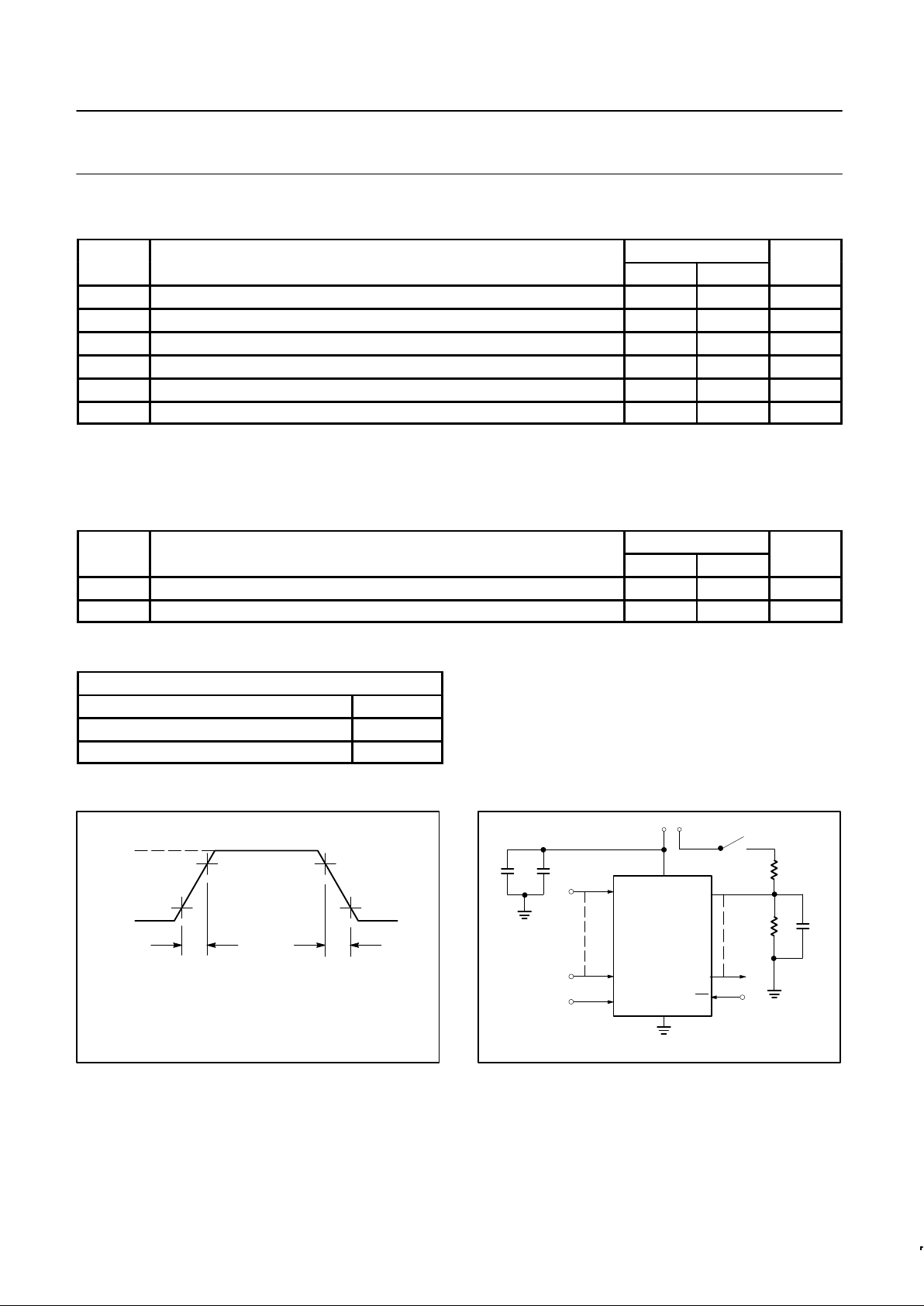
VOLTAGE WAVEFORM
90%
10%
1.5ns1.5ns
+3.0V
0V
t
R
t
F
MEASUREMENTS:
All circuit delays are measured at the +1.5V level of
inputs and outputs, unless otherwise specified.
Input Pulses
SP00368
TEST LOAD CIRCUIT
+5V
C
L
R
1
R
2
S
1
C
2
C
1
NOTE:
C
1
and C2 are to bypass VCC to GND.
V
CC
GND
CK
I
n
I
0
F
0
F
n
DUT
OE
INPUTS
SP00369
Philips Semiconductors Product specification
ABT22V10A5, A7
5V high-speed universal PLD device
with live insertion capability
1996 Dec 16
4
DC ELECTRICAL CHARACTERISTICS
Over operating ranges.
LIMITS
SYMBOL
PARAMETER
TEST CONDITIONS
1
MIN MAX
UNIT
Input voltage
V
IL
Low VCC = MIN 0.8 V
V
IH
High VCC = MAX 2.0 V
V
I
Clamp VCC = MIN, IIN = –18mA –1.2 V
Output voltage
V
CC
= MIN
IOH = –32mA 2.0 V
VOHHigh-level output voltage
VCC = MIN
VI = V
IH
or V
IL
IOH = –16mA 2.4 V
V
OL
Low-level output voltage
VCC = MIN
VI = VIH or V
IL
IOL = 48mA 0.5 V
Input current
I
IL
Low VCC = MAX, VIN = 0.4V –10 µA
I
IH
High VCC = MAX, VIN = 2.7V 10 µA
I
I
Max input current VCC = MAX, VIN = 5.5V 20 µA
Output current
I
PU/PD
Power-up/down 3-State
output current
4
VCC <2.1V; VO = 0.5V to VCC;
V
I
= GND or VCC; OE/OE = X
50 µA
VCC = MAX
I
OZH
Output leakage
2
VIN = VIL or VIH, V
OUT
= 2.7V 20 µA
I
OZL
Output leakage
2
VIN = VIL or VIH, V
OUT
=0.4V –20 µA
I
SC
Short circuit
3
V
OUT
= 0.5V –30 –220 mA
I
CC
VCC supply current VCC = MAX, Outputs enabled, VI = VCC or GND; IO = 0 200 mA
Ground Bounce TYP MAX UNIT
V
OLP
Minimum dynamic V
OH
5
VCC = MAX, 25°C
C
L
= 50pF (including jig capacitance)
1.0 1.2 V
NOTES:
1. These are absolute values with respect to device ground and all overshoots due to system or tester noise are included.
2. I/O pin leakage is the worst case of I
OZX
or IIX (where X = H or L).
3. No more than one output should be tested at a time. Duration of the short-circuit test should not exceed one second. V
OUT
= 0.5V has been
chosen to avoid test problems caused by tester ground degradation.
4. This parameter is valid for any V
CC
between 0V and 1.2 V with a transition time up to 10 mS. From VCC = 1.2 to VCC = 5.0V ±0.25V a
transition time of 100 µS is permitted. X = Don’t care.
5. Guaranteed by design, but not tested. Measured holding one output (the output under test) Low and simultaneously switching all remianing
output from a High to a Low state. Switch S1 is closed; 50pF load.
Philips Semiconductors Product specification
ABT22V10A5, A7
5V high-speed universal PLD device
with live insertion capability
1996 Dec 16
5
AC ELECTRICAL CHARACTERISTICS
1
4.75V ≤ V
CC
≤ 5.25V; 0C ≤ T
amb
≤ +75C
LIMITS
SYMBOL
PARAMETER
TEST
CONDITIONS
ABT22V10A5 ABT22V10A7
UNIT
CONDITIONS
MIN TYP MAX MIN TYP MAX
Input or feedback to
Active-LOW 2.0 4.5 5.0 2.0 6.0 7.5 ns
t
PD
Input or feedback to
non-registered output
2
Active-HIGH 2.0 4.5 5.0 2.0 6.0 7.5 ns
t
S
Setup time from input or SP
to Clock
2.0 1.3 3.5 3.0 ns
t
SIO
Setup time from feedback
to Clock
2.25 1.5 3.5 3.0 ns
t
H
Hold time 0 0 ns
t
SKEWR
Skew between registered
outputs
4, 7
1.0 1.0 ns
t
CO
Clock to output 2.0 3.5 4.0 2.0 4.5 5.5 ns
t
CF
Clock to feedback
3
2.0 4.0 3.0 5.0 ns
t
AR
Asynchronous Reset to
registered output
10.0 10.0 ns
t
ARW
Asynchronous Reset width 6.0 7.5 ns
t
ARR
Asynchronous Reset
recovery time
4.0 5.5 ns
t
SPR
Synchronous Preset
recovery time
4.5 5.0 ns
t
WL
Width of Clock LOW 2.0 3.0 ns
t
WH
Width of Clock HIGH 2.0 3.0 ns
Maximum frequency;
External feedback
1/(t
S
+ tCO)
4
167 208 111 133 MHz
f
MAX
Maximum frequency;
Internal feedback
1/(t
S
+ tCF)
4
167 303 125 166 MHz
t
EA
Input to Output Enable
5
8.0 8.0 ns
t
ER
Input to Output Disable
5
7.5 7.5 ns
Capacitance
6
Input Capacitance (Pin 2) VIN = 2.0V
8 8 pF
C
IN
Input Capacitance (Others) VIN = 2.0V
VCC = 5.0V
T
amb
= 25°C
4 4 pF
C
OUT
Output Capacitance V
OUT
= 2.0V
f = 1MHz
8 8 pF
NOTES:
1. Test Conditions: R1 = 300Ω, R2 =390Ω
2. t
PD
is tested with switch S1 closed and CL = 50pF (including jig capacitance). VIH = 3V, VIL = 0V, VT = 1.5V.
3. Calculated from measured f
MAX
internal.
4. These parameters are not 100% tested, but are calculated at initial characterization and at any time the design is modified where frequency
may be affected.
5. For 3-State output; output enable times are tested with C
L
= 50pF to the 1.5V level, and S1 is open for high-impedance to High tests and
closed for high-impedance to Low tests. Output disable times are tested with C
L =
5pF. High-to-High impedance tests are made to an output
voltage of V
T
= (VOH – 0.5V) with S1 open, and Low-to-High impedance tests are made to the VT = (VOL + 0.5V) level with S1 closed.
6. These parameters are not 100% tested, but are evaluated at initial characterization and at any time the design is modified where
capacitance may be affected.
7. Skew is measured with all outputs switching in the same direction.

Philips Semiconductors Product specification
ABT22V10A5, A7
5V high-speed universal PLD device
with live insertion capability
1996 Dec 16
6
PRODUCT FEATURES
Low Ground Bounce
The Philips Semiconductors BiCMOS QUBiC process produces
exceptional noise immunity. The typical ground bounce, with 9
outputs simultaneously switching and the 10th output held low, is
less than 1.0V. V
OLP
is tested by holding one output (the output
uncer test) in the Low state and then simultaneously switching all
remaining outputs from a High to a Low state (each output is loaded
with 50pF). The maximum peak voltage on the output under test is
guaranteed to be less than 1.2 Volts.
Live Insertion/Extraction Capability
There are some inherent problems associated with inserting or
extracting an unpowered module from a powered-up, active system.
The ABT22V10A outputs have been designed such that any chance
of bus contention, glitching or clamping is eliminated.
Detailed information on this feature is provided in an application note
AN051:
Philips PLDs Support Live Insertion Applications
.
Improved Fuse Verification Circuitry Increases
Reliability
Philips has developed a new means of testing the integrity of fuses,
both blown and intact fuses, which insures that all the fuses have
been correctly programmed and that each and every fuse – whether
“blown” or “intact” – is at the appropriate and optimal fuse
resistance. This dual verify scheme represents a significant
improvement over single reference voltage comparisons schemes
that have been used for bipolar devices since the late 1980s.
Detailed information on this feature is provided in an application note
entitled
Dual Verify Technique Increases Reliability of PLDs
.
Programmable 3-stage Outputs
Each output has a 3-Stage output buffer with 3-State control. A
product term controls the buffer, allowing enable and disable to be a
function of any product of device inputs or output feedback. The
combinatorial output provides a bidirectional I/O pin, and may be
configured as a dedicated input if the buffer is always disabled.
Programmable Output Polarity
The polarity of each macro cell output can be Active-HIGH or
Active-LOW, either to match output signal needs or to reduce
product terms. Programmable polarity allows Boolean expressions
to be written in their most compact form (true or inverted), and the
output can still be of the desired polarity. It can also save
“DeMorganizing” efforts.
Selection is controlled by programmable bit S
0
in the Output Macro
Cell, and affects both registered and combinatorial outputs.
Selection is automatic, based on the design specification and pin
definitions. If the pin definition and output equation have the same
polarity, the output is programmed to be Active-HIGH (S
0
= 1).
Preset/Reset
For initialization, the ABT22V10A has additional Preset and Reset
product terms. These terms are connected to all registered outputs.
When the Synchronous Preset (SP) product term is asserted high,
the output registers will be loaded with a HIGH on the next
LOW-to-HIGH clock transition. When the Asynchronous Reset (AR)
product term is asserted high, the output registers will be
immediately loaded with a LOW, independent of the clock.
Note that Preset and Reset control the flip-flop, not the output pin.
The output level is determined by the output polarity selected.
Power-Up Reset
All flip-flops power-up to a logic LOW for predictable system
initialization. Outputs of the ABT22V10A will depend on the
programmed output polarity. The V
CC
rise must be monotonic and
the reset delay time is 1–10µs maximum.
Security Fuse
After programming and verification, ABT22V10A designs can be
secured by programming the security fuse link. Once programmed,
this fuse defeats readback of the internal programmed pattern by a
device programmer, securing proprietary designs from competitors.
When the security fuse is programmed, the array will read as if
every fuse is programmed.
Quality and Testability
The ABT22V10A offers a very high level of built-in quality. Extra
programmable fuses provide a means of verifying performance of all
AC and DC parameters. In addition, this verifies programmability
and functionality of the device to provide the highest programming
and post-programming functional yields.
Technology
The BiCMOS ABT22V10A is fabricated with the Philips
Semiconductors process known as QUBiC. QUBiC combines an
advanced, state-of-the-art 1.0µm (drawn feature size) CMOS
process with an ultra fast bipolar process to achieve superior speed
and drive capabilities. QUBiC incorporates three layers of Al/Cu
interconnects for reduced chip size, and our proven Ti-W fuse
technology ensures highest programming yields.
Programming
The ABT22V10A is fully supported by industry standard (JEDEC
compatible) PLD CAD tools, including Philips Semiconductors
SNAP design software package. ABEL
CUPL and PALASM 90
design software packages also support the ABT22V10A
architecture.
All packages allow Boolean and state equation entry formats, SNAP,
ABEL and CUPL also accept, as input, schematic capture format.
Output Register Preload
The register on the ABT22V10A can be preloaded from the output
pins to facilitate functional testing of complex state machine designs.
This feature allows direct loading of arbitrary states, making it
unnecessary to cycle through long test vector sequences to reach a
desired state. In addition, transitions from illegal states can be
verified by loading illegal states and observing proper recovery. The
procedure for preloading follows:
1. Raise V
CC
to 5.0V ± 0.25V.
2. Set pin 2 or 3 to V
HH
to disable outputs and enable preload.
3. Apply the desired value (V
ILP/VIHP
) to all registered output pins.
Leave combinatorial output pins floating.
4. Clock Pin 1 from V
ILP
to V
IHP
.
5. Remove V
ILP/VIHP
from all registered output pins.
6. Lower pin 2 or 3 to V
ILP
.
7. Enable the output registers according to the programmed
pattern.
8. Verify V
OL/VOH
at all registered output pins. Note that the output
pin signal will depend on the output polarity.
ABEL is a trademark of Data I/O Corp.
CUPL is a trademark of Logical Devices, Inc.
PALASM is a registered trademark of AMD Corp.
 Loading...