

Philips 89C51, 89C52, 89C54, 89C58 Technical data

查询P89C51BA供应商
INTEGRATED CIRCUITS
89C51/89C52/89C54/89C58
80C51 8-bit microcontroller family
4K/8K/16K/32K Flash
Product data
Supersedes data of 1999 Oct 27
IC28 Data Handbook
2002 Jan 15

Philips Semiconductors Product data
80C51 8-bit microcontroller family
4K/8K/16K/32K Flash
DESCRIPTION
The 89C51/89C52/89C54/89C58 contain a non-volatile FLASH
program memory that is parallel programmable. For devices that are
serial programmable (In-System Programmable (ISP) and
In-Application Programmable (IAP) with a boot loader), see the
89C51Rx2 or 89C66x datasheets.
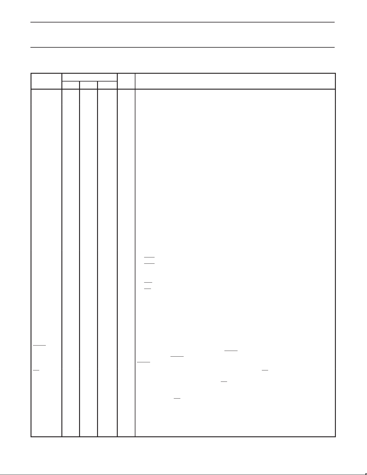
SELECTION T ABLE FOR FLASH DEVICES
MTP devices
(this data sheet)
89C51 89C52/54/58 89C51Rx2 89C66x
ROM/EPROM memory size 4K 8K/16K/32K 16K–64K 16K–64K
RAM size (byte) 128 256 512–1K 512–8K
Parallel programming yes yes yes yes
In-System Programming (ISP) no no yes yes
In-Application Programming (IAP) no no yes yes
PWM no no yes yes
Programmable Timer/Counter (PCA) no no yes yes
Hardware Watchdog Timer no no yes yes
Serial Channels UART UART UART UART + I2C
All three families are Single-Chip 8-bit Microcontrollers
manufactured in advanced CMOS process and are derivatives of
the 80C51 microcontroller family. All the devices have the same
instruction set as the 80C51.
89C51/89C52/89C54/89C58
ISP/IAP devices
(see separate data sheets)
MTP = Multi-Time Programming (via parallel programmer)
ISP = In-System Programming (via serial interface)
IAP = In-Application Programming
Please note that the FLASH programming algorithm for these parts has been modified. Please see the Device Comparison table for details.
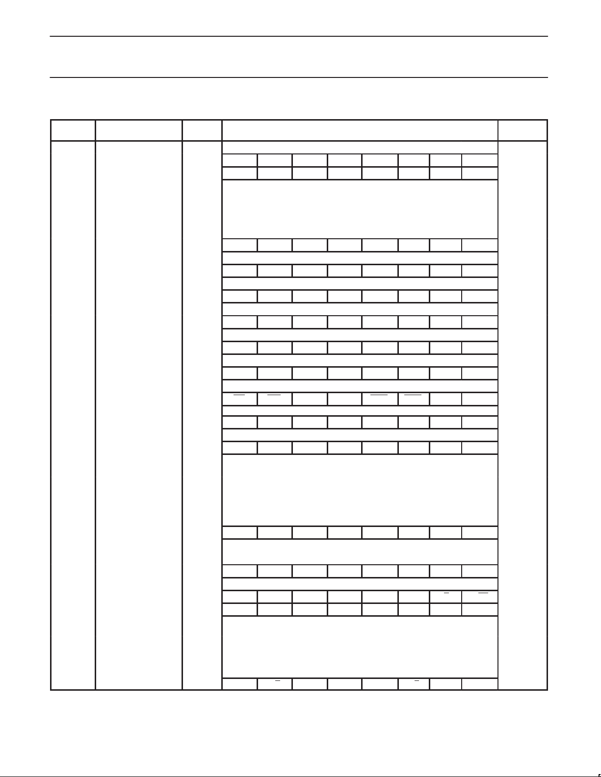
DEVICE COMPARISON TABLE
Item Old devices New devices Reason for change
Type description P89C5xUBxx / P89C5xUFxx P89C5xBx Letter U dropped for shorter type
Programming algorithm When using parallel programmer,
Quad Flat Package type PQFP package (P89C5xUxBB) PQFP package replaced by
Package identifiers PLCC = AA
Flash memory program and
erase cycles
Power consumption Active mode: I
be sure to select P89C5xUxxx
devices
PQFP = BB
PDIP = PN
100 program and erase cycles 10,000 program and erase
=
(0.9 FREQ. + 20)mA
Idle mode: I
(0.37 FREQ. + 1.0)mA
CC(MAX)
CC(MAX)
=
When using a parallel programmer, be sure to select P89C5xBx
devices (no more letter U). IF
DEVICES ARE NOT YET SELECTABLE, ASK YOUR VENDOR FOR A SOFTWARE UPDATE.
LQFP package (P89C5xBBD).
SEE NEW DIMENSIONS AT
THE END OF THIS DATA
SHEET.
PLCC = A
LQFP = BD
PDIP = P
cycles
Active mode: I
(0.55 FREQ. + 8.0)mA
Idle mode: I
(0.3 FREQ. + 2.0)mA
CC(MAX)
CC(MAX)
=
=
descriptions (formerly designated
speed (0–33 MHz))
Programming algorithm modification required by process change!
Reduction in package height
Shorter type descriptions
Process change allows more program and erase cycles
Process change allows lower
power consumption
2002 Jan 15 853–2148 27548
2
Philips Semiconductors Product data
Frequency
(MHz)
80C51 8-bit microcontroller family
4K/8K/16K/32K Flash
FEATURES
•80C51 Central Processing Unit
•On-chip FLASH Program Memory
•Speed up to 33 MHz
•Fully static operation
•RAM expandable externally up to 64 kbytes
•4 interrupt priority levels
•6 interrupt sources
•Four 8-bit I/O ports
•Full-duplex enhanced UART
– Framing error detection
– Automatic address recognition
ORDERING INFORMATION
Type number Package
4K Flash
version
P89C51BA P89C52BA P89C54BA P89C58BA PLCC44 plastic leaded chip
P89C51BP
P89C51BN
P89C51BBD P89C52BBD P89C54BBD P89C58BBD LQFP44 plastic low profile quad
NOTES:
1. Philips (except North America) Part Order Number
2. Philips North America Part Order Number. Note that parts will be marked “P89C5xBP”, respectively (x = 1, 2, 4, 8)
3. Industrial temperatures will be released with P89C5xX2 devices (see separate data sheet)
1
2
8K Flash
version
P89C52BP
P89C52BN
1
2
16K Flash
version
P89C54BP
P89C54BN
1
2
32K Flash
version
P89C58BP
P89C58BN
Name Description Version
1
DIP40 plastic dual in-line
2
carrier; 44 leads
package; 40 leads
flat package; 44 leads;
body 10 x 10 x 1.4 mm
•Three 16-bit timers/counters T0, T1 (standard 80C51) and
additional T2 (capture and compare)
•Power control modes
– Clock can be stopped and resumed
– Idle mode
– Power down mode
•Programmable clock out
•Second DPTR register
•Asynchronous port reset
•Low EMI (inhibit ALE)
•Wake up from power down by an external interrupt
89C51/89C52/89C54/89C58
Temperature
Range3 (°C) Range (V)
SOT187-2 0 to +70 5 0 to 33
SOT129-1 0 to +70 5 0 to 33
SOT389-1 0 to +70 5 0 to 33
Voltage
P ART NUMBER DERIVATION
Device number (P89C5x) Temperature range Package
P89C51
P89C52
P89C54
P89C58
2002 Jan 15
B = 0 _C to 70 _C
3
BD = LQFP
A = PLCC
P = PDIP
Philips Semiconductors Product data
80C51 8-bit microcontroller family
4K/8K/16K/32K Flash
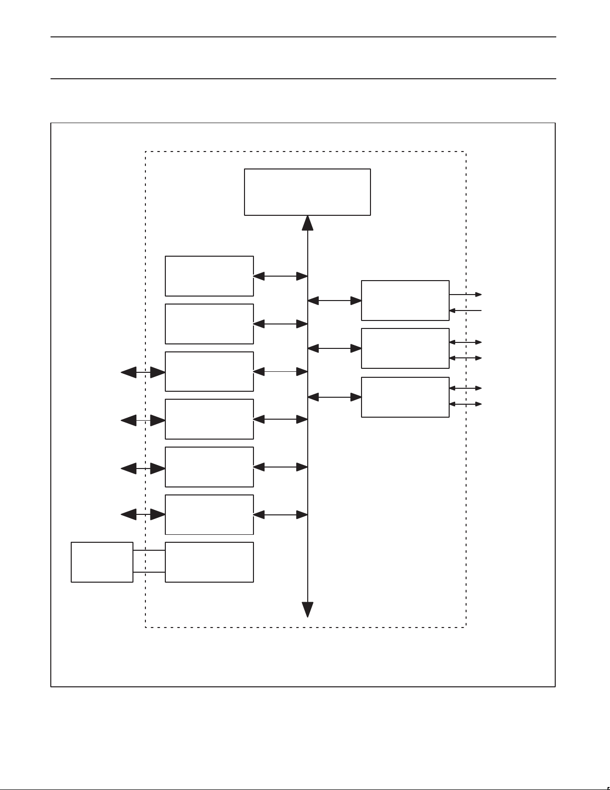
BLOCK DIAGRAM 1
4K – 32K Byte
Code Flash
128 / 256 Byte
Data RAM
Port 3
Configurable I/Os
89C51/89C52/89C54/89C58
Standard 80C51+
CPU
Full-duplex enhanced
UART
Timer 0
Timer 1
Timer 2
Resonator
Port 2
Configurable I/Os
Port 1
Configurable I/Os
Port 0
Configurable I/Os
OscillatorCrystal or
su01554
2002 Jan 15
4
Philips Semiconductors Product data
80C51 8-bit microcontroller family
4K/8K/16K/32K Flash
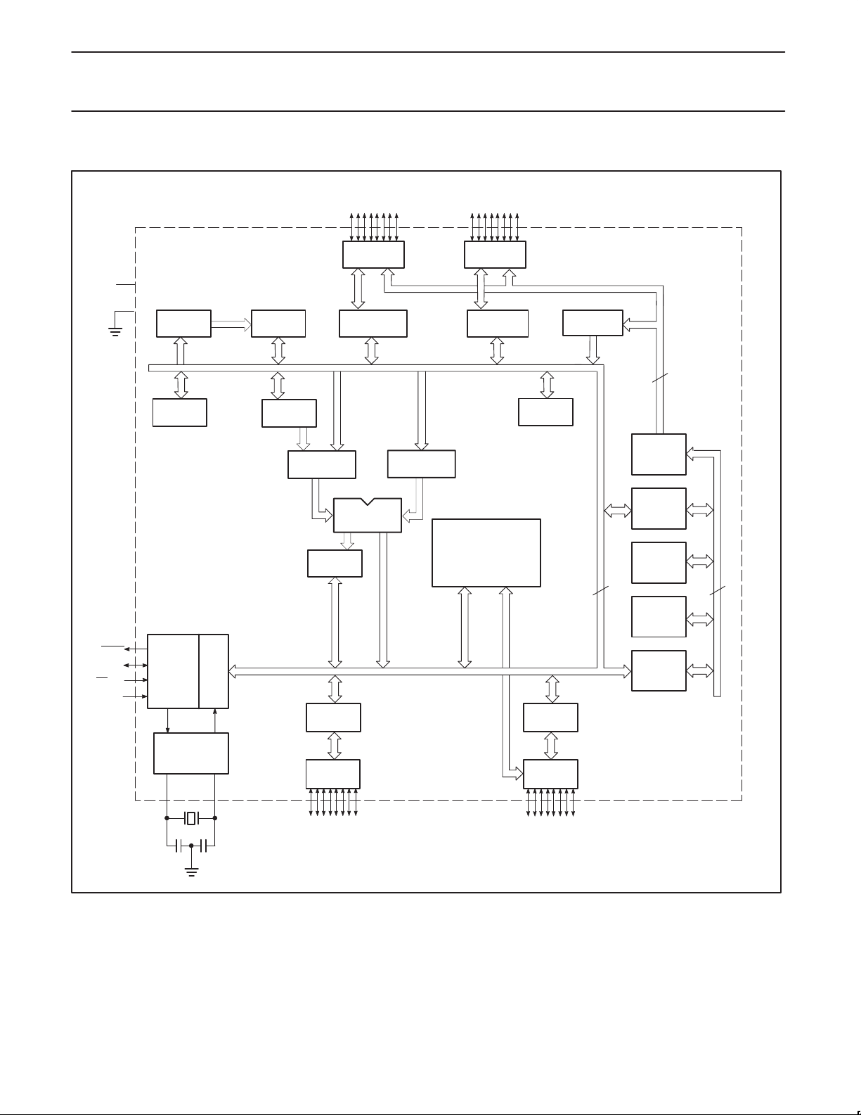
BLOCK DIAGRAM 2 (CPU ORIENTED)
V
CC
V
SS
RAM ADDR
REGISTER
B
REGISTER
RAM
ACC
TMP2
P0.0–P0.7 P2.0–P2.7
PORT 0
DRIVERS
PORT 0
LATCH
TMP1
PORT 2
DRIVERS
PORT 2
LATCH
89C51/89C52/89C54/89C58
FLASH
8
STACK
POINTER
PROGRAM
ADDRESS
REGISTER
PSEN
EAV
ALE
PP
RST
TIMING
AND
CONTROL
OSCILLATOR
XTAL1 XTAL2
INSTRUCTION
PD
REGISTER
PSW
PORT 1
LATCH
PORT 1
DRIVERS
P1.0–P1.7
ALU
SFRs
TIMERS
PORT 3
LATCH
PORT 3
DRIVERS
P3.0–P3.7
BUFFER
PC
INCRE-
MENTER
8 16
PROGRAM
COUNTER
DPTR’S
MULTIPLE
SU01066
2002 Jan 15
5
Philips Semiconductors Product data
80C51 8-bit microcontroller family
4K/8K/16K/32K Flash
LOGIC SYMBOL
V
V
SS
CC
XTAL1
ADDRESS AND
PORT 0
XTAL2
RST
EA/V
PP
PSEN
ALE/PROG
RxD
TxD
INT0
INT1
T0
PORT 3
T1
WR
RD
SECONDARY FUNCTIONS
PIN CONFIGURA TIONS
Dual In-Line Package Pin Functions
DATA BUS
T2
T2EX
PORT 1PORT 2
ADDRESS BUS
SU00830
89C51/89C52/89C54/89C58
Ceramic and Plastic Leaded Chip Carrier
Pin Functions
6140
7
17
Pin Function
1 NIC*
2 P1.0/T2
3 P1.1/T2EX
4 P1.2
5 P1.3
6 P1.4
7 P1.5
8 P1.6
9 P1.7
10 RST
11 P3.0/RxD
12 NIC*
13 P3.1/TxD
14 P3.2/INT0
15 P3.3/INT1
* NO INTERNAL CONNECTION
PLCC
18 28
Pin Function
16 P3.4/T0
17 P3.5/T1
18 P3.6/WR
19 P3.7/RD
20 XTAL2
21 XTAL1
22 V
SS
23 NIC*
24 P2.0/A8
25 P2.1/A9
26 P2.2/A10
27 P2.3/A11
28 P2.4/A12
29 P2.5/A13
30 P2.6/A14
39
29
Pin Function
31 P2.7/A15
32 PSEN
33 ALE
34 NIC*
35 EA/V
36 P0.7/AD7
37 P0.6/AD6
38 P0.5/AD5
39 P0.4/AD4
40 P0.3/AD3
41 P0.2/AD2
42 P0.1/AD1
43 P0.0/AD0
44 V
PP
CC
SU01062
T2/P1.0
T2EX/P1.1
P1.2
P1.3
P1.4
P1.5
P1.6
P1.7
RST
RxD/P3.0
TxD/P3.1
INT0
/P3.2
/P3.3
INT1
T0/P3.4
T1/P3.5
/P3.6
WR
RD
/P3.7
XTAL2
XTAL1
V
40
39
38
37
36
35
34
33
32
31
30
29
28
27
26
25
24
23
22
21
SU01063
V
CC
P0.0/AD0
P0.1/AD1
P0.2/AD2
P0.3/AD3
P0.4/AD4
P0.5/AD5
P0.6/AD6
P0.7/AD7
EA
/V
PP
ALE
PSEN
P2.7/A15
P2.6/A14
P2.5/A13
P2.4/A12
P2.3/A11
P2.2/A10
P2.1/A9
P2.0/A8
Low Profile Quad Flat Pack Pin Functions
44 34
1
11
Pin Function
1 P1.5
2 P1.6
3 P1.7
4 RST
5 P3.0/RxD
6 NIC*
7 P3.1/TxD
8 P3.2/INT0
9 P3.3/INT1
10 P3.4/T0
11 P3.5/T1
12 P3.6/WR
13 P3.7/RD
14 XTAL2
15 XTAL1
* NO INTERNAL CONNECTION
LQFP
12 22
Pin Function
16 V
SS
17 NIC*
18 P2.0/A8
19 P2.1/A9
20 P2.2/A10
21 P2.3/A11
22 P2.4/A12
23 P2.5/A13
24 P2.6/A14
25 P2.7/A15
26 PSEN
27 ALE
28 NIC*
29 EA
/V
30 P0.7/AD7
PP
33
23
Pin Function
31 P0.6/AD6
32 P0.5/AD5
33 P0.4/AD4
34 P0.3/AD3
35 P0.2/AD2
36 P0.1/AD1
37 P0.0/AD0
38 V
CC
39 NIC*
40 P1.0/T2
41 P1.1/T2EX
42 P1.2
43 P1.3
44 P1.4
SU01494
1
2
3
4
5
6
7
8
9
DUAL
10
IN-LINE
PACKAGE
11
12
13
14
15
16
17
18
19
20
SS
2002 Jan 15
6
Philips Semiconductors Product data
80C51 8-bit microcontroller family
4K/8K/16K/32K Flash
PIN DESCRIPTIONS
PIN NUMBER
MNEMONIC DIP LCC QFP TYPE NAME AND FUNCTION
V
SS
V
CC
P0.0–0.7 39–32 43–36 37–30 I/O Port 0: Port 0 is an open-drain, bidirectional I/O port. Port 0 pins that have 1s written to
P1.0–P1.7 1–8 2–9 40–44,
P2.0–P2.7 21–28 24–31 18–25 I/O Port 2: Port 2 is an 8-bit bidirectional I/O port with internal pull-ups. Port 2 pins that have 1s
P3.0–P3.7 10–17 11,
RST 9 10 4 I Reset: A high on this pin for two machine cycles while the oscillator is running, resets the
ALE 30 33 27 O Address Latch Enable: Output pulse for latching the low byte of the address during an
PSEN 29 32 26 O Program Store Enable: The read strobe to external program memory. When executing
EA/V
PP
XTAL1 19 21 15 I Crystal 1: Input to the inverting oscillator amplifier and input to the internal clock
XTAL2 18 20 14 O Crystal 2: Output from the inverting oscillator amplifier.
NOTE: To avoid “latch-up” effect at power-on, the voltage on any pin (other than VPP) at any time must not be higher than VCC + 0.5 V or
V
– 0.5 V , respectively.
SS
20 22 16 I Ground: 0 V reference.
40 44 38 I Power Supply: This is the power supply voltage for normal, idle, and power-down operation.
them float and can be used as high-impedance inputs. Port 0 is also the multiplexed
low-order address and data bus during accesses to external program and data memory. In
this application, it uses strong internal pull-ups when emitting 1s.
1–3
1 2 40 I/O T2 (P1.0): T imer/Counter2 external count input/clockout (see Programmable Clock-Out).
2 3 41 I T2EX (P1.1): Timer/Counter2 reload/capture/direction control.
13–195,7–13
10 11 5 I RxD (P3.0): Serial input port
11 13 7 O TxD (P3.1): Serial output port
12 14 8 I INT0 (P3.2): External interrupt
13 15 9 I INT1 (P3.3): External interrupt
14 16 10 I T0 (P3.4): Timer 0 external input
15 17 11 I T1 (P3.5): Timer 1 external input
16 18 12 O WR (P3.6): External data memory write strobe
17 19 13 O RD (P3.7): External data memory read strobe
31 35 29 I External Access Enable/Programming Supply Voltage: EA must be externally held low
I/O Port 1: Port 1 is an 8-bit bidirectional I/O port with internal pull-ups. Port 1 pins that have 1s
written to them are pulled high by the internal pull-ups and can be used as inputs. As inputs,
port 1 pins that are externally pulled low will source current because of the internal pull-ups.
(See DC Electrical Characteristics: I
written to them are pulled high by the internal pull-ups and can be used as inputs. As inputs,
port 2 pins that are externally being pulled low will source current because of the internal
pull-ups. (See DC Electrical Characteristics: I
during fetches from external program memory and during accesses to external data memory
that use 16-bit addresses (MOVX @DPTR). In this application, it uses strong internal
pull-ups when emitting 1s. During accesses to external data memory that use 8-bit addresses
(MOV @Ri), port 2 emits the contents of the P2 special function register.
I/O Port 3: Port 3 is an 8-bit bidirectional I/O port with internal pull-ups. Port 3 pins that have 1s
written to them are pulled high by the internal pull-ups and can be used as inputs. As inputs,
port 3 pins that are externally being pulled low will source current because of the pull-ups.
(See DC Electrical Characteristics: I
89C51/89C52/89C54/89C58, as listed below:
device. An internal diffused resistor to V
capacitor to V
access to external memory. In normal operation, ALE is emitted at a constant rate of 1/6 the
oscillator frequency , and can be used for external timing or clocking. Note that one ALE
pulse is skipped during each access to external data memory. ALE can be disabled by
setting SFR auxiliary.0. With this bit set, ALE will be active only during a MOVX instruction.
code from the external program memory, PSEN
except that two PSEN
is not activated during fetches from internal program memory.
PSEN
to enable the device to fetch code from external program memory locations 0000H to the
maximum internal memory boundary. If EA
program memory unless the program counter contains an address greater than 0FFFH for
4 k devices, 1FFFH for 8 k devices, 3FFFH for 16 k devices, and 7FFFH for 32 k devices.
The value on the EA
have no effect. This pin also receives the 5V/12V (±10%) programming supply voltage (V
during FLASH programming.
generator circuits.
.
CC
activations are skipped during each access to external data memory.
pin is latched when RST is released and any subsequent changes
89C51/89C52/89C54/89C58
). Alternate function for Port 1:
IL
). Port 2 emits the high-order address byte
IL
). Port 3 also serves the special features of the
IL
permits a power-on reset using only an external
SS
is activated twice each machine cycle,
is held high, the device executes from internal
PP
)
2002 Jan 15
7
Philips Semiconductors Product data
80C51 8-bit microcontroller family
4K/8K/16K/32K Flash
Table 1. 89C51/89C52/89C54/89C58 Special Function Registers
SYMBOL DESCRIPTION
ACC* Accumulator E0H E7 E6 E5 E4 E3 E2 E1 E0 00H
AUXR# Auxiliary 8EH – – – – – – – AO xxxxxxx0B
AUXR1# Auxiliary 1 A2H – – – – GF2 0 – DPS xxxx00x0B
B* B register F0H F7 F6 F5 F4 F3 F2 F1 F0 00H
DPTR: Data Pointer (2 bytes)
DPH Data Pointer High 83H 00H
DPL Data Pointer Low 82H 00H
IE* Interrupt Enable A8H EA – ET2 ES ET1 EX1 ET0 EX0 0x000000B
IP* Interrupt Priority B8H – – PT2 PS PT1 PX1 PT0 PX0 xx000000B
IPH# Interrupt Priority High B7H – – PT2H PSH PT1H PX1H PT0H PX0H xx000000B
P0* Port 0 80H AD7 AD6 AD5 AD4 AD3 AD2 AD1 AD0 FFH
P1* Port 1 90H – – – – – – T2EX T2 FFH
P2* Port 2 A0H AD15 AD14 AD13 AD12 AD11 AD10 AD9 AD8 FFH
P3* Port 3 B0H RD WR T1 T0 INT1 INT0 TxD RxD FFH
DIRECT
ADDRESS
BIT ADDRESS, SYMBOL, OR ALTERNATIVE PORT FUNCTION
MSB LSB
AF AE AD AC AB AA A9 A8
BF BE BD BC BB BA B9 B8
B7 B6 B5 B4 B3 B2 B1 B0
87 86 85 84 83 82 81 80
97 96 95 94 93 92 91 90
A7 A6 A5 A4 A3 A2 A1 A0
B7 B6 B5 B4 B3 B2 B1 B0
89C51/89C52/89C54/89C58
RESET
VALUE
PCON#1Power Control 87H SMOD1 SMOD0 – POF
D7 D6 D5 D4 D3 D2 D1 D0
PSW* Program Status Word D0H CY AC F0 RS1 RS0 OV – P 000000x0B
RACAP2H# Timer 2 Capture High CBH 00H
RACAP2L# Timer 2 Capture Low CAH 00H
SADDR# Slave Address A9H 00H
SADEN# Slave Address Mask B9H 00H
SBUF Serial Data Buffer 99H xxxxxxxxB
9F 9E 9D 9C 9B 9A 99 98
SCON* Serial Control 98H
SP Stack Pointer 81H 07H
TCON* Timer Control 88H TF1 TR1 TF0 TR0 IE1 IT1 IE0 IT0 00H
T2CON* Timer 2 Control C8H TF2 EXF2 RCLK TCLK EXEN2 TR2 C/T2 CP/RL2 00H
T2MOD# Timer 2 Mode Control C9H – – – – – – T2OE DCEN xxxxxx00B
TH0 Timer High 0 8CH 00H
TH1 Timer High 1 8DH 00H
TH2# Timer High 2 CDH 00H
TL0 Timer Low 0 8AH 00H
TL1 Timer Low 1 8BH 00H
TL2# Timer Low 2 CCH 00H
TMOD Timer Mode 89H GATE C/T M1 M0 GATE C/T M1 M0 00H
* SFRs are bit addressable.
# SFRs are modified from or added to the 80C51 SFRs.
– Reserved bits.
1. Reset value depends on reset source.
2. Bit will not be affected by reset.
SM0/FE
8F 8E 8D 8C 8B 8A 89 88
CF CE CD CC CB CA C9 C8
SM1 SM2 REN TB8 RB8 TI RI 00H
2
GF1 GF0 PD IDL 00xxx000B
2002 Jan 15
8

Philips Semiconductors Product data
80C51 8-bit microcontroller family
4K/8K/16K/32K Flash
FLASH EPROM MEMORY
General Description
The 89C51/89C52/89C54/89C58 FLASH reliably stores memory
contents even after 10,000 erase and program cycles. The cell is
designed to optimize the erase and programming mechanisms. In
addition, the combination of advanced tunnel oxide processing and
low internal electric fields for erase and programming operations
produces reliable cycling.
Features
•FLASH EPROM internal program memory with Chip Erase
•Up to 64 k byte external program memory if the internal program
memory is disabled (EA
•Programmable security bits
•10,000 minimum erase/program cycles for each byte
•10 year minimum data retention
•Programming support available from many popular vendors
= 0)
89C51/89C52/89C54/89C58
OSCILLA T OR CHARACTERISTICS
XTAL1 and XTAL2 are the input and output, respectively, of an
inverting amplifier. The pins can be configured for use as an
on-chip oscillator.
To drive the device from an external clock source, XTAL1 should be
driven while XTAL2 is left unconnected. There are no requirements
on the duty cycle of the external clock signal, because the input to
the internal clock circuitry is through a divide-by-two flip-flop.
However, minimum and maximum high and low times specified in
the data sheet must be observed.
RESET
A reset is accomplished by holding the RST pin high for at least two
machine cycles (24 oscillator periods), while the oscillator is running.
To insure a good power-on reset, the RST pin must be high long
enough to allow the oscillator time to start up (normally a few
milliseconds) plus two machine cycles. At power-on, the voltage on
V
and RST must come up at the same time for a proper start-up.
CC
Ports 1, 2, and 3 will asynchronously be driven to their reset
condition when a voltage above V
The value on the EA
no further effect.
pin is latched when RST is deasserted and has
(min.) is applied to RST.
IH1
2002 Jan 15
9
Philips Semiconductors Product data
80C51 8-bit microcontroller family
4K/8K/16K/32K Flash
LOW POWER MODES
Stop Clock Mode
The static design enables the clock speed to be reduced down to
0 MHz (stopped). When the oscillator is stopped, the RAM and
Special Function Registers retain their values. This mode allows
step-by-step utilization and permits reduced system power
consumption by lowering the clock frequency down to any value. For
lowest power consumption the Power Down mode is suggested.
Idle Mode
In the idle mode (see Table 2), the CPU puts itself to sleep while all
of the on-chip peripherals stay active. The instruction to invoke the
idle mode is the last instruction executed in the normal operating
mode before the idle mode is activated. The CPU contents, the
on-chip RAM, and all of the special function registers remain intact
during this mode. The idle mode can be terminated either by any
enabled interrupt (at which time the process is picked up at the
interrupt service routine and continued), or by a hardware reset
which starts the processor in the same manner as a power-on reset.
Power-Down Mode
To save even more power, a Power Down mode (see Table 2) can
be invoked by software. In this mode, the oscillator is stopped and
the instruction that invoked Power Down is the last instruction
executed. The on-chip RAM and Special Function Registers retain
their values down to 2.0 V and care must be taken to return V
the minimum specified operating voltages before the Power Down
Mode is terminated.
Either a hardware reset or external interrupt can be used to exit from
Power Down. Reset redefines all the SFRs but does not change the
on-chip RAM. An external interrupt allows both the SFRs and the
on-chip RAM to retain their values.
To properly terminate Power Down the reset or external interrupt
should not be executed before V
operating level and must be held active long enough for the
oscillator to restart and stabilize (normally less than 10ms).
With an external interrupt, INT0 and INT1 must be enabled and
configured as level-sensitive. Holding the pin low restarts the oscillator
but bringing the pin back high completes the exit. Once the interrupt
is serviced, the next instruction to be executed after RETI will be the
one following the instruction that put the device into Power Down.
is restored to its normal
CC
Design Consideration
When the idle mode is terminated by a hardware reset, the device
normally resumes program execution, from where it left off, up to
CC
to
89C51/89C52/89C54/89C58
two machine cycles before the internal reset algorithm takes control.
On-chip hardware inhibits access to internal RAM in this event, but
access to the port pins is not inhibited. To eliminate the possibility of
an unexpected write when Idle is terminated by reset, the instruction
following the one that invokes Idle should not be one that writes to a
port pin or to external memory.
ONCE Mode
The ONCE (“On-Circuit Emulation”) Mode facilitates testing and
debugging of systems without the device having to be removed from
the circuit. The ONCE Mode is invoked by:
1. Pull ALE low while the device is in reset and PSEN
2. Hold ALE low as RST is deactivated.
While the device is in ONCE Mode, the Port 0 pins go into a float
state, and the other port pins and ALE and PSEN
high. The oscillator circuit remains active. While the device is in this
mode, an emulator or test CPU can be used to drive the circuit.
Normal operation is restored when a normal reset is applied.
Programmable Clock-Out
A 50% duty cycle clock can be programmed to come out on P1.0.
This pin, besides being a regular I/O pin, has two alternate
functions. It can be programmed:
1. to input the external clock for Timer/Counter 2, or
2. to output a 50% duty cycle clock ranging from 61Hz to 4MHz at a
16MHz operating frequency.
To configure the Timer/Counter 2 as a clock generator, bit C/T
T2CON) must be cleared and bit T20E in T2MOD must be set. Bit
TR2 (T2CON.2) also must be set to start the timer.
The Clock-Out frequency depends on the oscillator frequency and
the reload value of Timer 2 capture registers (RCAP2H, RCAP2L)
as shown in this equation:
Oscillator Frequency
4 (65536 * RCAP2H,RCAP2L)
Where (RCAP2H,RCAP2L) = the content of RCAP2H and RCAP2L
taken as a 16-bit unsigned integer.
In the Clock-Out mode Timer 2 roll-overs will not generate an
interrupt. This is similar to when it is used as a baud-rate generator.
It is possible to use Timer 2 as a baud-rate generator and a clock
generator simultaneously. Note, however, that the baud-rate and the
Clock-Out frequency will be the same.
is high;
are weakly pulled
2 (in
Table 2. External Pin Status During Idle and Power-Down Mode
MODE PROGRAM MEMORY ALE PSEN PORT 0 PORT 1 PORT 2 PORT 3
Idle Internal 1 1 Data Data Data Data
Idle External 1 1 Float Data Address Data
Power-down Internal 0 0 Data Data Data Data
Power-down External 0 0 Float Data Data Data
2002 Jan 15
10

Philips Semiconductors Product data
80C51 8-bit microcontroller family
4K/8K/16K/32K Flash
TIMER 0 AND TIMER 1 OPERATION
Timer 0 and Timer 1
The “Timer” or “Counter” function is selected by control bits C/T in
the Special Function Register TMOD. These two Timer/Counters
have four operating modes, which are selected by bit-pairs (M1, M0)
in TMOD. Modes 0, 1, and 2 are the same for both Timers/Counters.
Mode 3 is different. The four operating modes are described in the
following text.
Mode 0
Putting either Timer into Mode 0 makes it look like an 8048 T imer,
which is an 8-bit Counter with a divide-by-32 prescaler. Figure 2
shows the Mode 0 operation as it applies to Timer 1.
In this mode, the Timer register is configured as a 13-bit register . As
the count rolls over from all 1s to all 0s, it sets the Timer interrupt
flag TF1. The counted input is enabled to the Timer when TR1 = 1
and either GA TE = 0 or INT1
Timer to be controlled by external input INT1
measurements). TR1 is a control bit in the Special Function Register
TCON (Figure 3). GATE is in TMOD.
The 13-bit register consists of all 8 bits of TH1 and the lower 5 bits
of TL1. The upper 3 bits of TL1 are indeterminate and should be
ignored. Setting the run flag (TR1) does not clear the registers.
Mode 0 operation is the same for the Timer 0 as for Timer 1.
Substitute TR0, TF0, and INT0
signals in Figure 2. There are two different GA TE bits, one for Timer
1 (TMOD.7) and one for Timer 0 (TMOD.3).
= 1. (Setting GATE = 1 allows the
, to facilitate pulse width
for the corresponding Timer 1
89C51/89C52/89C54/89C58
Mode 1
Mode 1 is the same as Mode 0, except that the Timer register is
being run with all 16 bits.
Mode 2
Mode 2 configures the Timer register as an 8-bit Counter (TL1) with
automatic reload, as shown in Figure 4. Overflow from TL1 not only
sets TF1, but also reloads TL1 with the contents of TH1, which is
preset by software. The reload leaves TH1 unchanged.
Mode 2 operation is the same for Timer/Counter 0.
Mode 3
Timer 1 in Mode 3 simply holds its count. The effect is the same as
setting TR1 = 0.
Timer 0 in Mode 3 establishes TL0 and TH0 as two separate
counters. The logic for Mode 3 on Timer 0 is shown in Figure 5. TL0
uses the Timer 0 control bits: C/T
the INT0
cycles) and takes over the use of TR1 and TF1 from Timer 1. Thus,
TH0 now controls the “Timer 1” interrupt.
Mode 3 is provided for applications requiring an extra 8-bit timer on
the counter. With Timer 0 in Mode 3, an 80C51 can look like it has
three Timer/Counters. When Timer 0 is in Mode 3, Timer 1 can be
turned on and off by switching it out of and into its own Mode 3, or
can still be used by the serial port as a baud rate generator, or in
fact, in any application not requiring an interrupt.
pin. TH0 is locked into a timer function (counting machine
, GATE, TR0, and TF0, as well as
TMOD Address = 89H Reset Value = 00H
Not Bit Addressable
76543 2 1 0
GATE C/T M1
TIMER 1 TIMER 0
GATE Gating control when set. Timer/Counter “x” is enabled only while “INTx” pin is high and
“TRx” control pin is set. when cleared Timer “x” is enabled whenever “TRx” control bit is set.
C/T Timer or Counter Selector cleared for Timer operation (input from in=ternal system clock.)
Set for Counter operation (input from “Tx” input pin).
M1 M0 OPERATING
0 0 8048 Timer “TLx” serves as 5-bit prescaler.
0 1 16-bit Timer/Counter “THx” and “TLx” are cascaded; there is no prescaler.
1 0 8-bit auto-reload Timer/Counter “THx” holds a value which is to be reloaded
into “TLx” each time it overflows.
1 1 (Timer 0) TL0 is an 8-bit Timer/Counter controlled by the standard Timer 0 control bits.
TH0 is an 8-bit timer only controlled by Timer 1 control bits.
1 1 (Timer 1) Timer/Counter 1 stopped.
Figure 1. Timer/Counter 0/1 Mode Control (TMOD) Register
M0 GA TE C/T
M1 M0
SU01514
2002 Jan 15
11
Philips Semiconductors Product data
80C51 8-bit microcontroller family
4K/8K/16K/32K Flash
OSC ÷ 12
C/T = 0
C/T = 1
T1 Pin
TR1
Gate
INT1 Pin
Figure 2. Timer/Counter 0/1 Mode 0: 13-Bit Counter (Timer 1 shown)
TCON Address = 88H Reset Value = 00H
Bit Addressable
Control
89C51/89C52/89C54/89C58
TL1
(5 Bits)
TH1
(8 Bits)
TF1 Interrupt
SU01555
76543210
IE0IT1IE1TR0TF0TR1TF1
IT0
BIT SYMBOL FUNCTION
TCON.7 TF1 Timer 1 overflow flag. Set by hardware on Timer/Counter overflow.
Cleared by hardware when processor vectors to interrupt routine, or clearing the bit in software.
TCON.6 TR1 Timer 1 Run control bit. Set/cleared by software to turn Timer/Counter on/off.
TCON.5 TF0 Timer 0 overflow flag. Set by hardware on Timer/Counter overflow.
Cleared by hardware when processor vectors to interrupt routine, or by clearing the bit in software.
TCON.4 TR0 Timer 0 Run control bit. Set/cleared by software to turn Timer/Counter on/off.
TCON.3 IE1 Interrupt 1 Edge flag. Set by hardware when external interrupt edge detected.
Cleared when interrupt processed.
TCON.2 IT1 Interrupt 1 type control bit. Set/cleared by software to specify falling edge/low level triggered
external interrupts.
TCON.1 IE0 Interrupt 0 Edge flag. Set by hardware when external interrupt edge detected.
Cleared when interrupt processed.
TCON.0 IT0 Interrupt 0 Type control bit. Set/cleared by software to specify falling edge/low level
triggered external interrupts.
Figure 3. Timer/Counter 0/1 Control (TCON) Register
SU01516
2002 Jan 15
12
 Loading...