

Philips 80c550, 83c550, 87c550 DATASHEETS

INTEGRATED CIRCUITS
80C550/83C550/87C550
80C51 8-bit microcontroller family
4K/128 OTP/ROM/ROMless, 8 channel 8 bit A/D,
watchdog timer
Product specification
Supersedes data of 1998 Jan 19
IC20 Data Handbook
1998 May 01

Philips Semiconductors Product specification
80C51 8-bit microcontroller family
4K/128 OTP/ROM/ROMless, 8 channel 8 bit A/D, watchdog timer
DESCRIPTION
The Philips 8XC550 is a high-performance microcontroller fabricated
with Philips high-density CMOS technology. This Philips CMOS
technology combines the high speed and density characteristics of
HMOS with the low power attributes of CMOS. Philips epitaxial
substrate minimizes latch-up sensitivity . The CMOS 8XC550 has the
same instruction set as the 80C51.
The 8XC550 contains a 4k × 8 EPROM (87C550)/ROM
(83C550)/ROMless (80C550 has no program memory on-chip), a
128 × 8 RAM, 8 channels of 8-bit A/D, four 8-bit ports (port 1 is input
only), a watchdog timer, two 16-bit counter/timers, a seven-source,
two-priority level nested interrupt structure, a serial I/O port for either
multi-processor communications, I/O expansion or full duplex UART,
and an on-chip oscillator and clock circuits.
In addition, the 8XC550 has two software selectable modes of
power reduction—idle mode and power-down mode. The idle mode
freezes the CPU while allowing the RAM, timers, serial port, and
interrupt system to continue functioning. The power-down mode
saves the RAM contents but freezes the oscillator, causing all other
chip functions to be inoperative.
FEA TURES
•80C51 based architecture
– 4k × 8 EPROM (87C550)/ROM (83C550)
– 128 × 8 RAM
– Eight channels of 8-bit A/D
– Two 16-bit counter/timers
– Watchdog timer
– Full duplex serial channel
– Boolean processor
•Memory addressing capability
– 64k ROM and 64k RAM
•Power control modes:
– Idle mode
– Power-down mode
•CMOS and TTL compatible
•One speed range at V
– 3.5 to 16MHz
•Extended temperature ranges
•OTP package available
80C550/83C550/87C550
= 5V ±10%
CC
ORDERING INFORMATION
TEMPERATURE RANGE °C
ROMless ROM EPROM
P80C550EBP N P83C550EBP N P87C550EBP N OTP 0 to +70, Plastic Dual In-Line Package 3.5 to 16 SOT129-1
P80C550EBA A P83C550EBA A P87C550EBA A OTP 0 to +70, Plastic Leaded Chip Carrier 3.5 to 16 SOT187-2
P80C550EFA A P83C550EFA A P87C550EFA A OTP –40 to +85, Plastic Leaded Chip Carrier 3.5 to 16 SOT187-2
NOTES:
1. OTP = One Time Programmable EPROM.
AND PACKAGE
1
FREQ
MHz
DRAWING
NUMBER
1998 May 01 853-1568 19329
2

Philips Semiconductors Product specification
80C51 8-bit microcontroller family
4K/128 OTP/ROM/ROMless, 8 channel 8 bit A/D, watchdog timer
BLOCK DIAGRAM
P0.0–P0.7 P2.0–P2.7
PORT 0
DRIVERS
V
CC
V
SS
RAM ADDR
REGISTER
B
REGISTER
RAM
ACC
TMP2
PORT 0
LATCH
TMP1
PORT 2
DRIVERS
PORT 2
LATCH
80C550/83C550/87C550
ROM/EPROM
STACK
POINTER
PROGRAM
ADDRESS
REGISTER
PSEN
ALE/PROG
EA/V
PP
RST
TIMING
AND
CONTROL
OSCILLATOR
XTAL1 XTAL2
INSTRUCTION
PD
REGISTER
PSW
PORT 1
LATCH
PORT 1
DRIVERS
P1.0–P1.7
ALU
PCON SCON TMOD TCON
TH0 TL0 TH1
TL1
SBUF IE IP
INTERRUPT, SERIAL
PORT AND TIMER BLOCKS
PORT 3
LATCH
PORT 3
DRIVERS
P3.0–P3.7
BUFFER
PC
INCRE-
MENTER
PROGRAM
COUNTER
DPTR
SU00005
1998 May 01
3
Philips Semiconductors Product specification
80C51 8-bit microcontroller family
4K/128 OTP/ROM/ROMless, 8 channel 8 bit A/D, watchdog timer
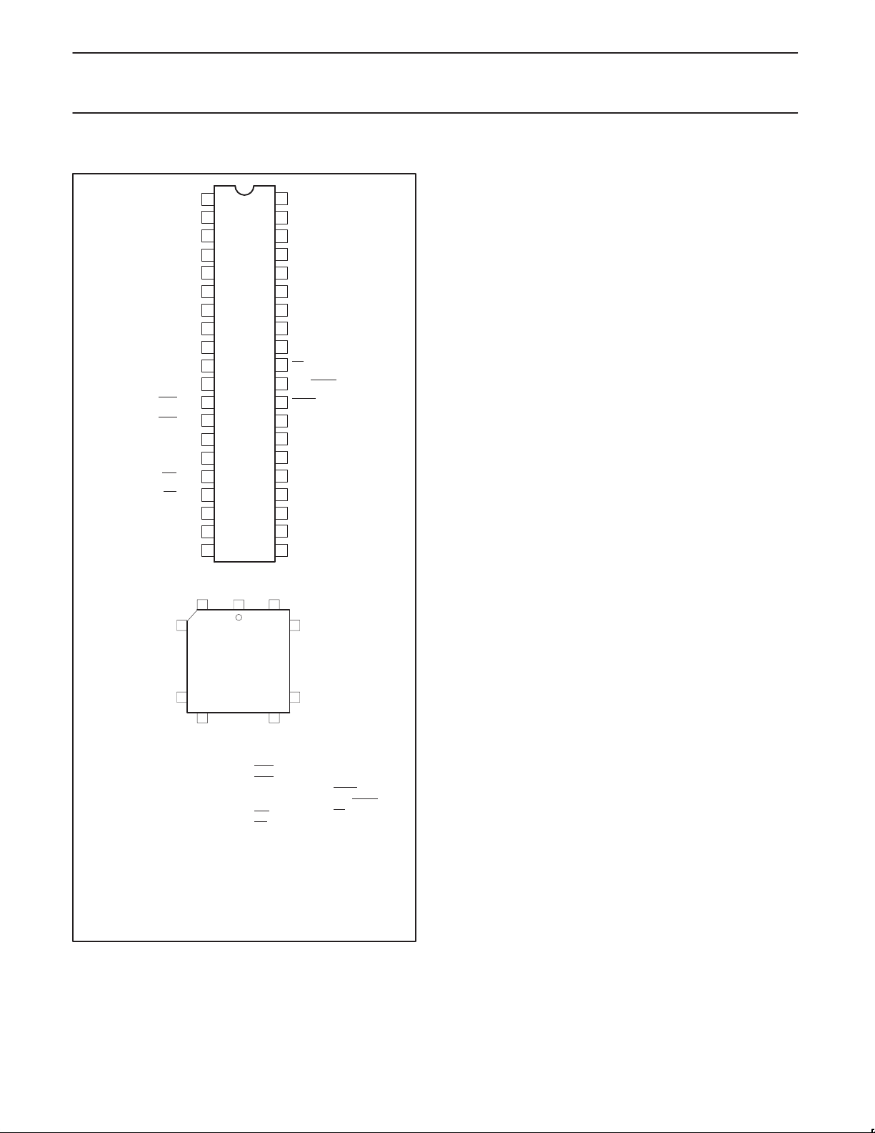
PIN CONFIGURATIONS
40
AVCC/Vref+
/Vref–
AV
SS
P1.0/ADC0
P1.1/ADC1
P1.2/ADC2
P1.3/ADC3
P1.4/ADC4
P1.5/ADC5
RST
RxD/P3.0
TxD/P3.1
INT0
/P3.2
INT1
/P3.3
T0/P3.4
T1/P3.5
WR
/P3.6
RD
/P3.7
XTAL2
XTAL1
V
1
2
3
4
5
6
7
8
9
PLASTIC
DUAL
10
IN-LINE
PACKAGE
11
12
13
14
15
16
17
18
19
20
SS
V
39
P0.0/AD0
38
P0.1/AD1
37
P0.2/AD2
36
P0.3/AD3
35
P0.4/AD4
34
P0.5/AD5
33
P0.6/AD6
32
P0.7/AD7
31
EA/V
30
ALE/PROG
29
PSEN
28
P2.7/A15
27
P2.6/A14
26
P2.5/A13
25
P2.4/A12
24
P2.3/A11
23
P2.2/A10
22
P2.1/A9
21
P2.0/A8
CC
PP
80C550/83C550/87C550
17
Pin Function
1AV
CC
2 Vref+
3 Vref–
4AV
SS
5 P1.0/ADC0
6 P1.1/ADC1
7 P1.2/ADC2
8 P1.3/ADC3
9 P1.4/ADC4
10 P1.5/ADC5
11 P1.6/ADC6
12 P1.7/ADC7
13 RST
14 P3.0/RxD
15 P3.1/TxD
6140
7
PLASTIC
LEADED
CHIP CARRIER
18 28
Pin Function
16 P3.2/INT0
17 P3.3/INT1
18 P3.4/T0
19 P3.5/T1
20 P3.6/WR
21 P3.7/RD
22 XTAL2
23 XTAL1
24 V
25 P2.0/A8
26 P2.1/A9
27 P2.2/A10
28 P2.3/A11
29 P2.4/A12
30 P2.5/A13
39
29
Pin Function
31 P2.6/A14
32 P2.7/A15
33 PSEN
34 ALE/PROG
35 EA/V
36 P0.7/AD7
37 P0.6/AD6
38 P0.5/AD5
SS
39 P0.4/AD4
40 P0.3/AD3
41 P0.2/AD2
42 P0.1/AD1
43 P0.0/AD0
44 V
PP
CC
SU00196
1998 May 01
4

Philips Semiconductors Product specification
80C51 8-bit microcontroller family
80C550/83C550/87C550
4K/128 OTP/ROM/ROMless, 8 channel 8 bit A/D, watchdog timer
PIN DESCRIPTION
PIN NO.
MNEMONIC DIP LCC TYPE NAME AND FUNCTION
V
SS
V
CC
AV
CC
AV
SS
Vref+
Vref–
P0.0–0.7 39–32 43–36 I/O Port 0: Port 0 is an open-drain, bidirectional I/O port. Port 0 pins that have 1s written to them float
P1.0–P1.7 3–8 5–12 I Port 1: Port 1 is an 8-bit input only port (6-bit in the DIP package; bits P1.6 and P1.7 are not
ADC0–ADC7 3–8 5–12 ADCx: Inputs to the analog multiplexer input of the 8-bit A/D. There are only six A/D inputs in the
P2.0–P2.7 21–28 25–32 I/O Port 2: Port 2 is an 8-bit bidirectional I/O port with internal pull-ups. Port 2 pins that have 1s written
P3.0–P3.7 10–17 14–21 I/O Port 3: Port 3 is an 8-bit bidirectional I/O port with internal pull-ups. Port 3 pins that have 1s written
RST 9 13 I Reset: A high on this pin for two machine cycles while the oscillator is running, resets the device.
ALE/PROG 30 34 I/O Address Latch Enable/Program Pulse: Output pulse for latching the low byte of the address
PSEN 29 33 O Program Store Enable: The read strobe to external program memory. When the device is
EA/V
PP
XTAL1 19 23 I Crystal 1: Input to the inverting oscillator amplifier and input to the internal clock generator circuits.
XTAL2 18 22 O Crystal 2: Output from the inverting oscillator amplifier.
20 24 I Ground: 0V reference.
40 44 I Power Supply: This is the power supply voltage for normal, idle, and power-down operation.
1 1 I Analog Power Supply: Analog supply voltage.
2 4 I Analog Ground: Analog 0V reference.
2
3
IIVref: A/D converter reference level inputs. Note that these references are combined with AVCC and
in the 40-pin DIP package.
AV
SS
and can be used as high-impedance inputs. Port 0 is also the multiplexed low-order address and
data bus during accesses to external program and data memory. In this application, it uses strong
internal pull-ups when emitting 1s. Port 0 also outputs the code bytes during program verification in
the S87C550. External pull-ups are required during program verification.
implemented). Port 1 digital input can be read out any time.
DIP package.
to them are pulled high by the internal pull-ups and can be used as inputs. As inputs, port 2 pins that
are externally being pulled low will source current because of the internal pull-ups. (See DC
Electrical Characteristics: I
program memory and during accesses to external data memory that use 16-bit addresses (MOVX
). Port 2 emits the high-order address byte during fetches from external
IL
@DPTR). In this application, it uses strong internal pull-ups when emitting 1s. During accesses to
external data memory that use 8-bit addresses (MOV @Ri), port 2 emits the contents of the P2
special function register.
to them are pulled high by the internal pull-ups and can be used as inputs. As inputs, port 3 pins that
are externally being pulled low will source current because of the pull-ups. (See DC Electrical
Characteristics: I
). Port 3 also serves the special features of the SC80C51 family, as listed below:
IL
10 14 I RxD (P3.0): Serial input port
11 15 O TxD (P3.1): Serial output port
12 16 I INT0 (P3.2): External interrupt
13 17 I INT1 (P3.3): External interrupt
14 18 I T0 (P3.4): Timer 0 external input
15 19 I T1 (P3.5): Timer 1 external input
16 20 O WR (P3.6): External data memory write strobe
17 21 O RD (P3.7): External data memory read strobe
An internal diffused resistor to V
.
V
CC
permits a power-on reset using only an external capacitor to
SS
during an access to external memory. In normal operation, ALE is emitted at a constant rate of 1/6
the oscillator frequency , and can be used for external timing or clocking. Note that one ALE pulse is
skipped during each access to external data memory. This pin is also the program pulse input
(PROG
) during EPROM programming.
executing code from the external program memory, PSEN
except that two PSEN
activations are skipped during each access to external data memory. PSEN
is activated twice each machine cycle,
is not activated during fetches from internal program memory.
31 35 I External Access Enable/Programming Supply Voltage: EA must be externally held low to enable
the device to fetch code from external program memory locations 0000H to 0FFFH. If EA
is held
high, the device executes from internal program memory unless the program counter contains an
address greater than 0FFFH. For the 80C550 ROMless part, EA
operate properly . This pin also receives the 12.75V programming supply voltage (V
EPROM programming.
must be held low for the part to
) during
PP
1998 May 01
5
Philips Semiconductors Product specification
80C51 8-bit microcontroller family
80C550/83C550/87C550
4K/128 OTP/ROM/ROMless, 8 channel 8 bit A/D, watchdog timer
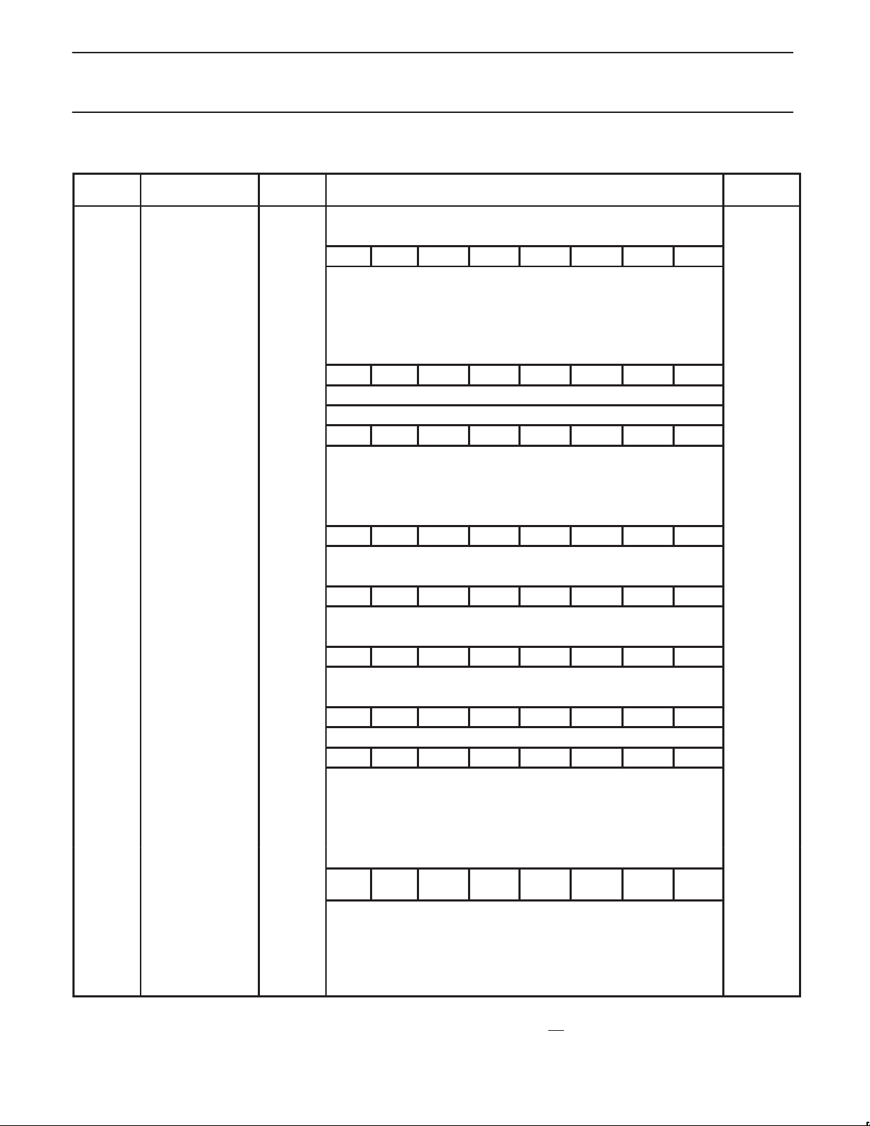
Table 1. 8XC550 Special Function Registers
SYMBOL DESCRIPTION
ACC* Accumulator E0H E7 E6 E5 E4 E3 E2 E1 E0 00H
ADAT# A/D result C6H xxH
ADCON# A/D control C5H – – – ADCI ADCS AADR2 AADR1 AADR0 xxx00000B
B* B register F0H F7 F6 F5 F4 F3 F2 F1 F0 00H
DPTR:
DPH
DPL
IP*# Interrupt priority B8H – PWD PAD PS PT1 PX1 PT0 PX0 x0000000B
IE*# Interrupt enable A8H EA EWD EAD ES ET1 EX1 ET0 EX0 00H
P0* Port 0 80H 87 86 85 84 83 82 81 80 FFH
P1* Port 1 90H 97 96 95 94 93 92 91 90 FFH
P2* Port 2 A0H A7 A6 A5 A4 A3 A2 A1 A0 FFH
P3* Port 3 B0H B7 B6 B5 B4 B3 B2 B1 B 0 FFH
PCON# Power control 87H SMOD SIDL – – GF1 GF0 PD IDL 00xx0000B
Data pointer
(2 bytes):
High byte
Low byte
DIRECT
ADDRESS
83H
82H
BIT ADDRESS, SYMBOL, OR ALTERNATIVE PORT FUNCTION
MSB LSB
BF BE BD BC BB BA B9 B8
AF AE AD AC AB AA A9 A8
RESET
VALUE
00H
00H
D7 D6 D5 D4 D3 D2 D1 D0
PSW* Program status word D0H CY AC F0 RS1 RS0 OV – P 00H
SBUF Serial data buffer 99H xxH
9F 9E 9D 9C 9B 9A 99 98
SCON* Serial port control 98H SM0 SM1 SM2 REN TB8 RB8 TI RI 00H
SP Stack pointer 81H 07H
8F 8E 8D 8C 8B 8A 89 88 00H
TCON* Timer counter/control 88H TF1 TR1 TF0 TR0 IE1 IT1 IE0 IT0 00H
TMOD Timer/counter mode 89H GATE C/T M1 M0 GATE C/T M1 M0 00H
TH0 Timer 0 high byte 8CH 00H
TH1 Timer 1 high byte 8DH 00H
TL0 Timer 0 low byte 8AH 00H
TL1 Timer 1 low byte 8BH 00H
C7 C6 C5 C4 C3 C2 C1 C0
WDCON*# Watchdog timer
control
WDL# Watchdog timer
reload
WFEED1# Watchdog timer
feed 1
WFEED2# Watchdog timer
feed 2
* SFRs are bit addressable.
# SFRs are modified from or added to the 80C51 SFRs.
**This value is not valid for a masked ROM part (83C550) when running from internal memory (EA
C0H PRE2 PRE1 PRE0 – –
C1H FFH**
C2H xxH
C3H xxH
WDRUN WDTOF
= 1). See data sheet for details.
WDMOD
000xx000B**
1998 May 01
6

Philips Semiconductors Product specification
80C51 8-bit microcontroller family
4K/128 OTP/ROM/ROMless, 8 channel 8 bit A/D, watchdog timer
SMOD SIDL X
BIT SYMBOL FUNCTION
PCON.7 SMOD Double baud rate
PCON.6 SIDL Serial port idle
PCON.5 X Reserved for future use
PCON.4 X Reserved for future use
PCON.3 GF1 General purpose flag bit
PCON.2 GF0 General purpose flag bit
PCON.1 PD Power down bit
PCON.0 IDL Idle mode bit
NOTE:
The PCON register is at SFR byte address 87H. Its contents following a reset are 00XX0000.
Figure 1. Power Control Register (PCON)
X GF1 GF0 PD IDL
80C550/83C550/87C550
LSBMSB
SU00197
LSBMSB
XXX
INPUT CHANNEL SELECTION
ADDR2 ADDR1 ADDR0 INPUT PIN
0 0 0 ADC0
0 0 1 ADC1
0 1 0 ADC2
0 1 1 ADC3
1 0 0 ADC4
1 0 1 ADC5
1 1 0 ADC6
1 1 1 ADC7
BIT SYMBOL FUNCTION
ADCON.7 — Not used
ADCON.6 — Not used
ADCON.5 — Not used
ADCON.4 ADCI ADC Interrupt flag.
This flag is set when an ADC conversion result is ready to be read. An interrupt is invoked if the
A/D interrupt is enabled. The flag must be cleared by software. It cannot be set by software.
ADCON.3 ADCS ADC Start and Status.
Setting this flag starts an A/D conversion. The ADC logic insures that this signal is high while the
ADC is busy. On completion of the conversion, ADCS is reset at the same time the interrupt flag
ADCI is set. ADCS cannot be reset by software.
ADCON.2 ADDR2 Analog Input Select 2
ADCON.1 ADDR1 Analog Input Select 1
ADCON.0 ADDR0 Analog Input Select 0
ADCI ADCS AADR2 AADR1 AADR0
SU00198
1998 May 01
Figure 2. A/D Control Register (ADCON)
7

Philips Semiconductors Product specification
80C51 8-bit microcontroller family
4K/128 OTP/ROM/ROMless, 8 channel 8 bit A/D, watchdog timer
A/D CONVERTER
The analog input circuitry consists of an 8-input analog multiplexer
and an analog-to-digital converter with 8-bit resolution. In the LCC
package, the analog reference voltage and analog power supplies
are connected via separate input pins; in the DIP package, Vref+ is
combined with AV
inputs are alternate functions to port 1, which is an input only port.
Digital input to port 1 can be read any time during an A/D
conversion. Care should be exercised in mixing analog and digital
signals on port 1, because cross talk from the digital input signals
can degrade the A/D conversion accuracy of the analog input. An
A/D conversion requires 40 machine cycles.
The A/D converter is controlled by the ADCON special function
register. The input channel to be converted is selected by the analog
multiplexer by setting ADCON register bits, ADDR2–ADDR0 (see
Figure 2). These bits can only be changed when ADCI and ADCS
are both low.
The completion of the 8-bit ADC conversion is flagged by ADCI in
the ADCON register and the result is stored in the special function
register ADAT.
An ADC conversion in progress is unaffected by a software ADC
start. The result of a completed conversion remains unaffected
provided ADCI remains at a logic 1. While ADCS is a logic 1 or
ADCI is a logic 1, a new ADC START will be blocked and
consequently lost. An A/D conversion in progress will be aborted
when the idle or power-down mode is entered. The result of a
completed conversion (ADCI = logic 1) remains unaffected when
entering the idle mode, but will be lost if power-down mode is
entered. See Figure 3 for the A/D input equivalent circuit.
The analog input pins ADC0-ADC7 may still be used as digital
inputs. The analog input channel that is selected by the
ADDR2-ADDR0 bits in ADCON cannot be used as a digital input.
Reading the selected A/D channel as a digital input will always
return a 1. The unselected A/D inputs may always be used as digital
inputs.
On RESET the A/D port pins are set to the Digital mode and will
work as a normal port and need no further initialization. To use the
A/D converter a single byte should be written to ADCON which
selects the A/D mux and concurrently sets the ADCS bit to start the
A/D conversion. The 40 machine cycles of the A/D conversion
include time for signal settling after the mux is selected and before
the Sample and Hold procedure is completed.
The circuitry which disables the digital buffer from the port pin is
updated at the start of an A/D conversion by setting the ADCS bit in
ADCON. After powerup, problems will occur the first time that
ADCON is written to if ADCS is not set; in this case, the digital
signal disable registers contain random data and some o the 8 port
pins will have their digital buffers disabled. When read, these
disabled buffers will ignore their input and only return a 1. This
condition will be corrected by writing a 1 to ADCS in ADCON which
starts and A/D conversion.
Thus, there are two operating modes:
1. DIGITAL ONLY - No Analog inputs are used and ADCON is
never written to. In this case pins ADC0-ADC7 are configured as
digital inputs.
2. A/D CONVERTER USED - The input multiplexer select field
must be written to and ADCS must be set in ADCON. This allows
unselected A/D inputs to be used as digital inputs.
and Vref– is combined with AVSS. The analog
CC
ADCON Register
ADCI ADCS Operation
*Not present on 40-pin DIP versions.
Symbol Position Function
ADCI ADCON.4 ADC interrupt flag. This flag is set when an
ADCS ADCON.3 ADC start and status. Setting this bit starts an
AADR2 ADCON.2 Analog input selects.
AADR1 ADCON.1 Binary coded address
AADR0 ADCON.0 selects one of the five analog input port pins of
80C550/83C550/87C550
MSB LSB
X X ADCI SDCS AADR2 AADR1 AADR0
X
0 0 ADC not busy, a conversion can be started.
0 1 ADC busy, start of a new conversion is blocked.
1 0 Conversion completed, start of a new is blocked.
1 1 Not possible.
INPUT CHANNEL SELECTION
ADDR2 ADDR1 ADDR0 INPUT PIN
0
0
0
0
1
1
1
1
0
0
1
1
0
0
1
1
ADC conversion is complete. If IE.5 = 1, an
interrupt is requested when ADCI = 1. The
ADCI flag must be cleared by software after
A/D data is read, before the next conversion
can begin.
A/D conversion. Once set, ADCS remains high
throughout the conversion cycle. On
completion of the conversion, it is reset at the
same time the ADCI interrupt flag is set. ADCS
cannot be reset by software.
P1 to be input to the converter. It can only be
changed when ADCI and ADCS are both l ow.
AADR2 is the most significant bit.
0
1
0
1
0
1
0
1
P1.0
P1.1
P1.2
P1.3
P1.4
P1.5
P1.6*
P1.7*
1998 May 01
8
Philips Semiconductors Product specification
80C51 8-bit microcontroller family
4K/128 OTP/ROM/ROMless, 8 channel 8 bit A/D, watchdog timer
Sample A/D Routines
The following routines demonstrate two methods of operating the
A/D converter. The first method uses polling to determine when the
A/D conversion is complete. The second method uses the A/D
interrupt to flag the end of conversion.
The routine ReadAD will start a read of the A/D channel identified by
R7, and wait for the conversion to complete, polling the A/D interrupt
flag. The result is returned in the accumulator.
ReadAD:MOV A,#08h ;Basic A/D start command.
ORL A,R7 ;Add channel # to be read.
MOV ADCON,A; ;Start A/D.
ADLoop: MOV A,ADCON ;Get A/D status.
JNB ACC.4,ADLoop;Wait for ADCI (A/D ;finished).
MOV A,ADAT ;Get conversion result
MOV ADCON,#0 ;Clear ADCI.
RET
The routine StartAD will start a read of the A/D channel identified by
R7 and exit back to the calling program. When the conversion is
complete, the A/D interrupt occurs, calling the A/D interrupt service
routine. The result of the conversion is returned in register R6.
StartAD: MOV A,#08h ;Basic A/D start command.
ADInt: MOV R6,ADAT ;Get conversion result.
80C550/83C550/87C550
ORL A,R7 ;Add channel # to be read.
MOV ADCON,A ;Start A/D.
RET
.
.
.
ORG 2Bh ;A/D interrupt address.
MOV ADCON,#0 ;Clear ADCI.
RETI
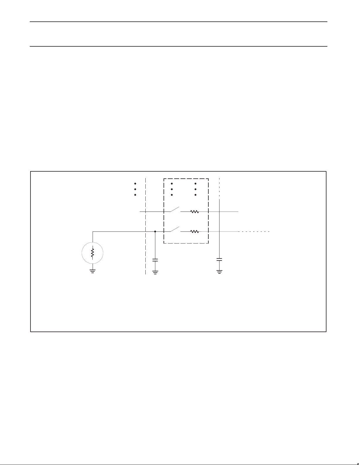
I
Sm
N+1
I
N
+
R
S
V
ANALOG
INPUT
Sm
C
S
N+1
N
Multiplexer
Rm
Rm
N+1
N
To Comparator
C
C
Rm = 0.5 - 3 kΩ
CS + CC = 15pF maximum
RS = Recommended < 9.6 kΩ for 1 LSB @ 12MHz
NOTE:
Because the analog to digital converter has a sampled-data comparator, the input looks capacitive to a source. When a conversion
is initiated, switch Sm closes for 8tcy (8µs @ 12MHz crystal frequency) during which time capacitance Cs + Cc is charged. It should
be noted that the sampling causes the analog input to present a varying load to an analog source.
SU00199
Figure 3. A/D Input: Equivalent Circuit
1998 May 01
9
 Loading...