

Philips 83c453, 87c453 DATASHEETS

INTEGRATED CIRCUITS
83C453/87C453
80C51 8-bit microcontroller family
8K/256 OTP/ROM, expanded I/O
Preliminary specification
Supersedes data of 1997 Dec 29
IC20 Data Handbook
1998 Apr 23

Philips Semiconductors Preliminary specification
80C51 8-bit microcontroller family
8K/256 OTP/ROM, expanded I/O
DESCRIPTION
The Philips 8XC453 is an I/O expanded single-chip microcontroller
fabricated with Philips high-density CMOS technology. Philips
epitaxial substrate minimizes latch-up sensitivity.
The 8XC453 is a functional extension of the 87C51 microcontroller
with three additional I/O ports and four I/O control lines. The 8XC453
is available in 68-pin LCC packages. Four control lines associated
with port 6 facilitate high-speed asynchronous I/O functions.
The 87C453 includes an 8k × 8 EPROM, a 256 × 8 RAM, 56 I/O
lines, two 16-bit timer/counters, a seven source, two priority level,
nested interrupt structure, a serial I/O port for either a full duplex
UART, I/O expansion, or multi-processor communications, and
on-chip oscillator and clock circuits.
The 87C453 has two software selectable modes of reduced activity
for further power reduction; idle mode and power-down mode. Idle
mode freezes the CPU while allowing the RAM, timers, serial port,
and interrupt system to continue functioning. Power-down mode
freezes the oscillator, causing all other chip functions to be
inoperative while maintaining the RAM contents.
83C453/87C453
FEA TURES
•80C51 based architecture
•Seven 8-bit I/O ports
•Port 6 features:
– Eight data pins
– Four control pins
– Direct MPU bus interface
– ISA Bus Interface
– Parallel printer interface
– IBF and OBF
– A flag latch on host write
•On the microcontroller:
– 8k × 8 EPROM
Quick pulse programming algorithm
Two-level program security system
– 256 × 8 RAM
– Two 16-bit counter/timers
– Two external interrupts
•External memory addressing capability
– 64k ROM and 64k RAM
•Low power consumption:
– Normal operation: less than 24mA at 5V , 16MHz
– Idle mode
– Power-down mode
•Reduced EMI
•Full-duplex enhanced UART
– Framing error detection
– Automatic address recognition
interrupts
ORDERING INFORMATION
1
EPROM
P87C453EBAA OTP P83C453EBAA 68–Pin Plastic Leaded Chip Carrier, 0 to +70 3.5 to 16 SOT188-3
NOTE:
1. OTP = One-Time Programmable EPROM.
1998 Apr 23
ROM TEMPERATURE °C AND PACKAGE
2
FREQ.
(MHz)
PKG. DWG
#
Philips Semiconductors Preliminary specification
80C51 8-bit microcontroller family
8K/256 OTP/ROM, expanded I/O
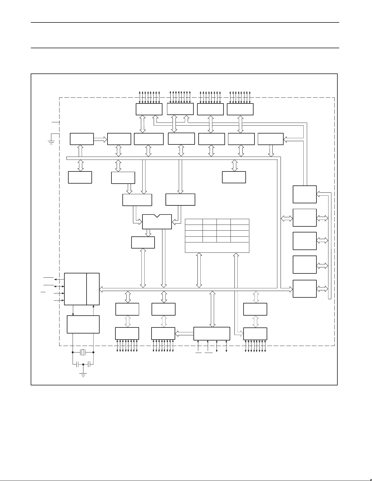
BLOCK DIAGRAM
P0.0–P0.7
PORT 0
DRIVERS
V
CC
V
SS
RAM ADDR
REGISTER
B
REGISTER
256 BYTES
RAM
ACC
TMP2
PORT 0
LATCH
P2.0–P2.7
PORT 2
DRIVERS
PORT 2
LATCH
TMP1
P4.0–P4.7
PORT 4
DRIVERS
PORT 4
LATCH
P5.0–5.7
PORT 5
DRIVERS
PORT 5
LATCH
STACK
POINTER
83C453/87C453
8K x 8
EPROM
PROGRAM
ADDRESS
REGISTER
PSEN
ALE/PROG
EAV
PP
RST
TIMING
AND
CONTROL
OSCILLATOR
XTAL1 XTAL2
INSTRUCTION
PD
REGISTER
PORT 1
LATCH
PORT 1
DRIVERS
P1.0–P1.7
PSW
ALU
PORT 6
LATCH
PORT 6
DRIVERS
P6.0–P6.7
PCON SCON TMOD TCON
TH0 TL0 TH1
PSW
TL1
DPH DPL AUXR
SBUF IE IP
CSR
INTERRUPT, SERIAL
PORT AND TIMER BLOCKS
PORT 6
CONTROL/STATUS
IDS ODS
AFLAG
BFLAG
PORT 3
LATCH
PORT 3
DRIVERS
P3.0–P3.7
BUFFER
PC
INCRE-
MENTER
PROGRAM
COUNTER
DPTR
SU00158
1998 Apr 23
3
Philips Semiconductors Preliminary specification
80C51 8-bit microcontroller family
8K/256 OTP/ROM, expanded I/O
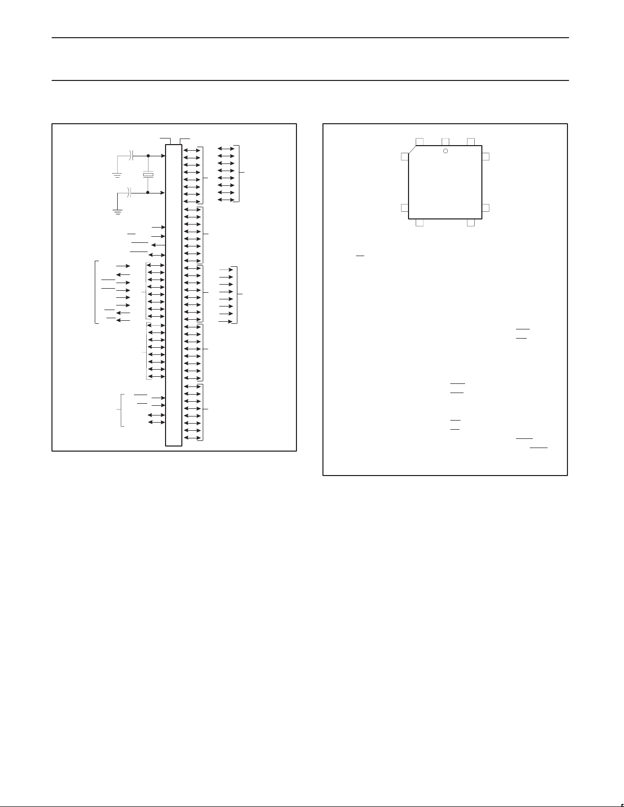
LOGIC SYMBOL
V
V
SS
CC
XTAL1
ADDRESS AND
PORT 0
XTAL2
RST
/V
EA
RxD
TxD
INT0
INT1
T0
T1
WR
RD
SECONDARY FUNCTIONS
PORT 6 CONTROL
PSEN
ALE/PROG
PORT 3
PORT 6
ODS
IDS
BFLAG
AFLAG
PP
PORT 1PORT 2
ADDRESS BUS
PORT 4
PORT 5
DATA BUS
SU00085
LCC PIN FUNCTIONS
10
26
27 43
Pin Function
/V
1EA
PP
2 P2.0/A8
3 P2.1/A9
4 P2.2/A10
5 P2.3/A11
6 P2.4/A12
7 P2.5/A13
8 P2.6/A14
9 P2.7/A15
10 P0.7/AD7
11 P0.6/AD6
12 P0.5/AD5
13 P0.4/AD4
14 P0.3/AD3
15 P0.2/AD2
16 P0.1/AD1
17 P0.0/AD0
18 V
CC
19 P4.7
20 P4.6
21 P4.5
22 P4.4
23 P4.3
Pin Function
24 P4.2
25 P4.1
26 P4.0
27 P1.0
28 P1.1
29 P1.2
30 P1.3
31 P1.4
32 P1.5
33 P1.6
34 P1.7
35 RST
36 P3.0/RxD
37 P3.1/TxD
38 P3.2/INTO
39 P3.3/INT1
40 P3.4/T0
41 P3.5/T1
42 P3.6/WR
43 P3.7/RD
44 P5.0
45 P5.1
46 P5.2
83C453/87C453
9161
LCC
60
44
Pin Function
47 P5.3
48 P5.4
49 P5.5
50 P5.6
51 P5.7
52 XTAL2
53 XTAL1
54 V
SS
55 ODS
56 IDS
57 BFLAG
58 AFLAG
59 P6.0
60 P6.1
61 P6.2
62 P6.3
63 P6.4
64 P6.5
65 P6.6
66 P6.7
67 PSEN
68 ALE/PROG
SU00157
1998 Apr 23
4

Philips Semiconductors Preliminary specification
80C51 8-bit microcontroller family
83C453/87C453
8K/256 OTP/ROM, expanded I/O
PIN DESCRIPTION
MNEMONIC
V
SS
V
CC
P0.0–0.7 17-10 I/O Port 0: Port 0 is an open-drain, bidirectional I/O port. Port 0 is also the multiplexed data and low-order
P1.0–P1.7 27-34 I/O Port 1: Port 1 is an 8-bit bidirectional I/O port with internal pull-ups. Port 1 receives the low-order address
P2.0–P2.7 2-9 I/O Port 2: Port 2 is an 8-bit bidirectional I/O port with internal pull-ups. Port 2 emits the high-order address
P3.0–P3.7 36-43 I/O Port 3: Port 3 is an 8-bit bidirectional I/O port with internal pull-ups. Port 3 can sink/source three LS TTL
P4.0–P4.3
P4.0–P4.7 26-19
P5.0–P5.7 44-51 I/O Port 5: Port 5 is an 8-bit bidirectional I/O port with internal pull-ups. Port 5 can sink/source three LS TTL
P6.0–P6.7 59-66 I/O Port 6: Port 6 is a specialized 8-bit bidirectional I/O port with internal pull-ups. This special port can
ODS 55 I ODS: Output data strobe
IDS 56 I IDS: Input data strobe
BFLAG 57 I/O BFLAG: Bidirectional I/O pin with internal pull-ups
AFLAG 58 I/O AFLAG: Bidirectional I/O pin with internal pull-ups
RST 35 I Reset: A high on this pin for two machine cycles while the oscillator is running, resets the device. An
ALE/PROG 68 I/O Address Latch Enable/Program Pulse: Output pulse for latching the low byte of the address during an
PSEN 67 O Program Store Enable: The read strobe to external program memory. PSEN is activated twice each
EA/V
PP
XTAL1 53 I Crystal 1: Input to the inverting oscillator amplifier that forms the oscillator. This input receives the external
XTAL2 52 O Crystal 2: An output of the inverting amplifier that forms the oscillator. This pin should be floated when an
PIN NO.
TYPE NAME AND FUNCTION
54 I Ground: 0V reference.
18 I Power Supply: This is the power supply voltage for normal, idle, and power-down operation.
address bus during accesses to external memory. External pull-ups are required during program
verification. Port 0 can sink/source eight LS TTL inputs.
bytes during program memory verification. Port 1 can sink/source three LS TTL inputs, and drive CMOS
inputs without external pull-ups.
bytes during access to external memory and receives the high-order address bits and control signals
during program verification. Port 2 can sink/source three LS TTL inputs, and drive CMOS inputs without
external pull-ups.
inputs, and drive CMOS inputs without external pull-ups. Port 3 also serves the special functions listed
below:
36 I RxD (P3.0): Serial input port
37 O TxD (P3.1): Serial output port
38 I INT0 (P3.2): External interrupt
39 I INT1 (P3.3): External interrupt
40 I T0 (P3.4): Timer 0 external input
41 I T1 (P3.5): Timer 1 external input
42 O WR (P3.6): External data memory write strobe
43 O RD (P3.7): External data memory read strobe
I/O
Port 4: Port 4 is an 8-bit bidirectional I/O port with internal pull-ups. Port 4 can sink/source three LS TTL
I/O
inputs and drive CMOS inputs without external pull-ups.
inputs and drive CMOS inputs without external pull-ups.
sink/source three LS TTL inputs and drive CMOS inputs without external pull-ups. Port 6 can be used in a
strobed or non-strobed mode of operation. Port 6 works in conjunction with four control pins that serve the
functions listed below:
internal pull-down resistor permits a power-on reset using only an external capacitor connected to VCC.
access to external memory. ALE is activated at a constant rate of 1/6 the oscillator frequency except during
an external data memory access, at which time one ALE is skipped. ALE can sink/source three LS TTL
inputs and drive CMOS inputs without external pull-ups. This pin is also the program pulse during EPROM
programming.
machine cycle during fetches from external program memory. However, when executing out of external
program memory, two activations of PSEN
PSEN
is not activated during fetches from internal program memory. PSEN can sink/source eight LS TTL
inputs and drive CMOS inputs without an external pull-up. This pin should be tied low during programming.
1 I Instruction Execution Control/Programming Supply Voltage: When EA is held high, the CPU executes
out of internal program memory, unless the program counter exceeds 1FFFH. When EA is held low, the
CPU executes out of external program memory. EA
the 12.75V programming supply voltage (V
oscillator when an external oscillator is used.
external oscillator is used.
are skipped during each access to external program memory.
must never be allowed to float. This pin also receives
) during EPROM programming.
PP
1998 Apr 23
5
Philips Semiconductors Preliminary specification
80C51 8-bit microcontroller family
83C453/87C453
8K/256 OTP/ROM, expanded I/O
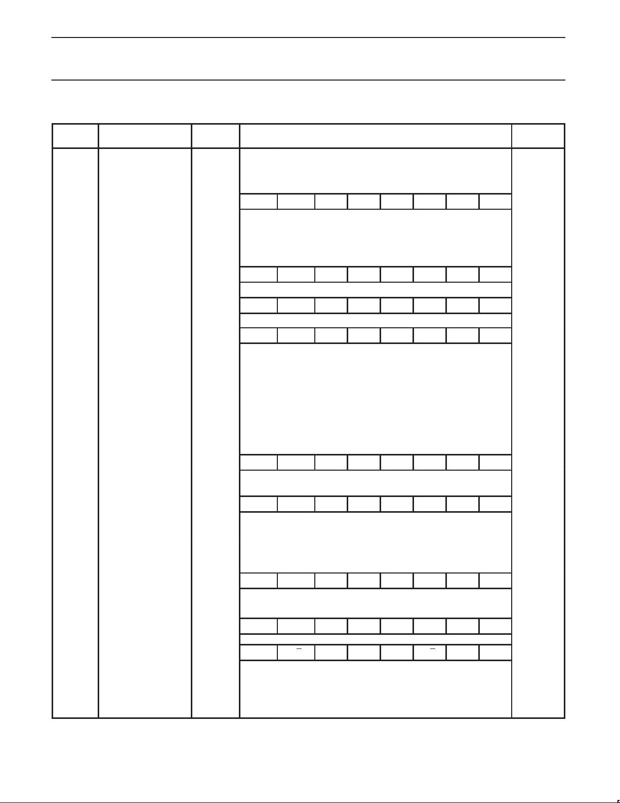
Table 1. 87C453 Special Function Registers
SYMBOL DESCRIPTION
ACC* Accumulator E0H E7 E6 E5 E4 E3 E2 E1 E0 00H
B* B register F0H F7 F6 F5 F4 F3 F2 F1 F0 00H
CSR*# Port 6 command/status E8H MB1 MB0 MA1 MA0 OBFC IDSM OBF IBF FCH
DPTR Data pointer (2 bytes)
DPH Data pointer high 83H 00H
DPL Data pointer low 82H 00H
IP* Interrupt priority B8H – POB PIB PS PT1 PX1 PT0 PX0 x0000000B
AUXR# Auxiliary register 8EH – – – – – – AF AO x0000000B
IE* Interrupt enable A8H EA IOB IIB ES ET1 EX1 ET0 EX0 00000000B
P0* Port 0 80H 87 B6 85 84 83 82 81 80 FFH
P1* Port 1 90H 97 96 95 94 93 92 91 90 FFH
P2* Port 2 A0H A7 A6 A5 A4 A3 A2 A1 A0 FFH
P3* Port 3 B0H B7 B6 B5 B4 B3 B2 B1 B0 FFH
P4*# Port 4 C0H C7 C6 C5 C4 C3 C2 C1 C0 FFH
P5*# Port 5 C8H CF CE CD CC CB CA C9 C8 FFH
P6*# Port 6 D8H DF DE DD DC DB DA D9 D8 FFH
DIRECT
ADDRESS
BIT NAMES AND ADDRESSES
MSB LSB
EF EE ED EC EB EA E9 E8
BF BE BD BC BB BA B9 B8
AF AE AD AC AB AA A9 A8
RESET
VALUE
PCON Power control 87H SMOD1 SMOD0 – POF1GF1 GF0 PD IDL 00xx0000B
D7 D6 D5 D4 D3 D2 D1 D0
PSW* Program status word D0H CY AC F0 RS1 RS0 OV – P 00H
SADDR# Slave Address A9H 00H
SADEN# Slave Address Mask B9H 00H
SBUF Serial data buffer 99H xxxxxxxxB
9F 9E 9D 9C 9B 9A 99 98
SCON* Serial port control 98H SM0 SM1 SM2 REN TB8 RB8 TI RI 00H
SP Stack pointer 81H 07H
8F 8E 8D 8C 8B 8A 89 88
TCON* Timer/counter control 88H TF1 TR1 TF0 TR0 IE1 IT1 IE0 IT0 00H
TMOD Timer/counter mode 89H GATE C/T M1 M0 GATE C/T M1 M0 00H
TH0 Timer 0 high byte 8CH 00H
TH1 Timer 1 high byte 8DH 00H
TL0 Timer 0 low byte 8AH 00H
TL1 Timer 1 low byte 8BH 00H
NOTES:
* SFRs are bit addressable.
# SFRs are modified from or added to the 80C51 SFRs.
1. REset value depends on reset source.
1998 Apr 23
6

Philips Semiconductors Preliminary specification
80C51 8-bit microcontroller family
8K/256 OTP/ROM, expanded I/O
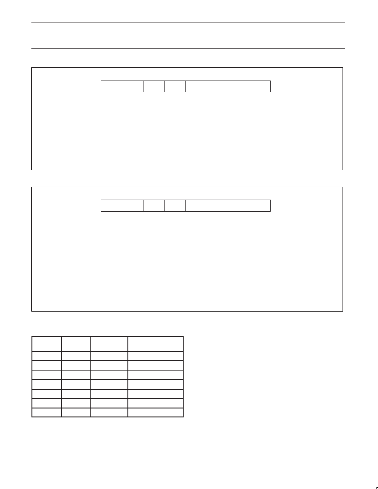
IE REGISTER IP REGISTER
INT0
TF0
INT1
TF1
RI
TI
0
IT0
1
0
IT1
1
IE.0
IE.1
IE.2
IE.3
IE.4
83C453/87C453
HIGH PRIORITY
INTERRUPT
INTERRUPT
POLLING
SEQUENCE
IBF
OBF
IE.5
IE.6
INDIVIDUAL
ENABLES
GLOBAL
DISABLE
Figure 1. 8XC453 Interrupt Control System
LSBMSB
ET0EX1ET1ESIIBIOBEA
EX0
BIT SYMBOL FUNCTION
IE.7 EA Disables all interrupts. If EA=0, no interrupt will be acknowledged. If EA=1, each interrupt
source is individually enabled or disabled by setting or clearing its enable bit.
IE.6 IOB Enables or disables the Output Buffer Full (OBF) interrupt. If IOB=0, the interrupt is disabled,
If IOB=1, an interrupt will occur if EA is set and data has been read from the output buffer
register through Port 6 by the external host pulsing ODS low.
IE.5 IIB Enables or disables the Input Buffer Full (IBF) interrupt. If IIB=0, the interrupt is disabled. If
IIB=1, an interrupt will occur if EA is set and data has been written into the Port 6 Input Data
Buffer by the host strobing IDS low .
IE.4 ES Enables or disables the Serial Port Interrupt. If ES=0, the Serial Port Interrupt. If ES=0, the
Serial Port interrupt is disabled.
IE.3 ET1 Enables or disables the Timer 1 Overflow interrupt. If ET1=0, the Timer 1 interrupt is disabled.
IE.2 EX1 Enables or disables External Interrupt 1. If EX1=0, External Interrupt 1 is disabled.
IE.1 ET0 Enables or disables the Timer 0 Overflow interrupt. If ET0=0, the Timer 0 interrupt is disabled.
IE.0 EX0 Enables or disables External Interrupt 0. If EX0=0, external Interrupt 0 is disabled.
Figure 2. 8XC453 Interrupt Enable (IE) Register
SU00563
LOW PRIORITY
INTERRUPT
SU00562
1998 Apr 23
7
Philips Semiconductors Preliminary specification
80C51 8-bit microcontroller family
83C453/87C453
8K/256 OTP/ROM, expanded I/O
LSBMSB
PT0PX1PT1PSPIBPOB—
BIT SYMBOL FUNCTION
IP.7 — Reserved.
IP.6 POB Defines the Output Buffer Full interrupt (IOB) priority level. POB=1 programs it to the higher priority level.
IP.5 PIB Defines the Input Buffer Full interrupt (IIB) priority level. PIB=1 programs it to the higher priority level.
IP.4 PS Defines the Serial Port interrupt priority level. PS=1 programs it to the higher priority level.
IP.3 PT1 Defines the Timer 1 interrupt priority level. PT1=1 programs it to the higher priority level.
IP.2 PX1 Defines the External Interrupt 1 priority level. PX1=1 programs it to the higher priority level.
IP.1 PT0 Enables or disables the Timer 0 interrupt priority level. PT0=1 programs it to the higher priority level.
IP.0 PX0 Defines the External Interrupt 0 priority level. PX0=1 programs it to the higher priority level.
Figure 3. 8XC453 Interrupt Priority (IP) Register
PDGF0GF1POF—SMOD2SMOD1
PX0
01234567
IDLPCON (87H)
SU00564
BIT SYMBOL FUNCTION
PCON.7 SMOD1 Double Baud rate bit. When set to a 1 and Timer 1 is used to generate baud rate, and the Serial Port
PCON.6 SMOD0 If set to 1, SCON.7 will be the Framing Error bit (FE). If PCON.6 is cleared, SCON.7 will be SM0.
PCON.5 — Reserved.
PCON.4 POF Power Off Flag is set during power on of V
PCON.3 GF1 General-purpose flag bit.
PCON.2 GF0 General-purpose flag bit.
PCON.1 PD Power-Down bit. Setting this bit activates power-down mode. It can only be set if input EW is high.
PCON.0 IDL Idle mode bit. Setting this bit activates the idle mode.
If logic 1s are written to PD and IDL at the same time, PD takes precedence.
is used in modes 1, 2, or 3.
if a warm start has occurred.
Figure 4. Power Control Register (PCON)
Table 2. Interrupt Table
POLLING
PRIORITY
1 INTO IE0 03H highest priority
2 Timer0 TF0 0BH
3 INT1 IE1 13H
4 Timer1 TF1 1BH
5 Port 6 OBF 33H
6 Serial I/O RI,TI 23H
7 Port 6 IBF 2BH lowest priority
SOURCE
REQUEST
BITS/FLAG
VECTOR
ADDRESS
. If then cleared by software, it can be used to determine
CC
SU00565
1998 Apr 23
8
 Loading...