

Philips 80c451, 83c451, 87c451 DATASHEETS

INTEGRATED CIRCUITS
80C451/83C451/87C451
80C51 8-bit microcontroller family
4K/128 OTP/ROM/ROMless, expanded I/O
Product specification
Supersedes data of 1998 Jan 19
IC20 Data Handbook
1998 May 01

Philips Semiconductors Product specification
80C51 8-bit microcontroller family
4K/128 OTP/ROM/ROMless, expanded I/O
DESCRIPTION
The Philips 8XC451 is an I/O expanded single-chip microcontroller
fabricated with Philips high-density CMOS technology. Philips
epitaxial substrate minimizes latch-up sensitivity.
The 8XC451 (includes the 80C451, 87C451 and 83C451) is a
functional extension of the 87C51 microcontroller with three
additional I/O ports and four I/O control lines for a total of 68 pins.
Four control lines associated with port 6 facilitate high-speed
asynchronous I/O functions.
The 8XC451 includes a 4k × 8 ROM (83C451) EPROM (87C451), a
128 × 8 RAM, 56 I/O, two 16-bit timer/counters, a five source, two
priority level, nested interrupt structure, a serial I/O port for either a
full duplex UART, I/O expansion, or multi-processor
communications, and on-chip oscillator and clock circuits. The
80C451 ROMless version includes all of the 83C451 features except
the on-board 4k × 8 ROM.
The 87C451 has 4k of EPROM on-chip as program memory and is
otherwise identical to the 83C451.
The 8XC451 has two software selectable modes of reduced activity
for further power reduction; idle mode and power-down mode. Idle
mode freezes the CPU while allowing the RAM, timers, serial port,
and interrupt system to continue functioning. Power-down mode
freezes the oscillator, causing all other chip functions to be
inoperative while maintaining the RAM contents.
FEA TURES
•80C51 based architecture
•Seven 8-bit I/O ports
•Port 6 features:
– Eight data pins
– Four control pins
– Direct MPU bus interface
– Parallel printer interface
•On the microcontroller:
– 4k × 8 ROM (83C451)
4k × 8 EPROM (87C451)
ROMless version (80C451)
– 128 × 8 RAM
– Two 16-bit counter/timers
– Two external interrupts
•External memory addressing capability
– 64k ROM and 64k RAM
•Low power consumption:
– Normal operation: less than 24mA at 5V , 12MHz
– Idle mode
– Power-down mode
80C451/83C451/87C451
PIN CONFIGURATION
9161
10
26
27 43
Pin Function
1EA
/V
PP
2 P2.0/A8
3 P2.1/A9
4 P2.2/A10
5 P2.3/A11
6 P2.4/A12
7 P2.5/A13
8 P2.6/A14
9 P2.7/A15
10 P0.7/AD7
11 P0.6/AD6
12 P0.5/AD5
13 P0.4/AD4
14 P0.3/AD3
15 P0.2/AD2
16 P0.1/AD1
17 P0.0/AD0
18 V
CC
19 P4.7
20 P4.6
21 P4.5
22 P4.4
23 P4.3
Pin Function
LCC
24 P4.2
25 P4.1
26 P4.0
27 P1.0
28 P1.1
29 P1.2
30 P1.3
31 P1.4
32 P1.5
33 P1.6
34 P1.7
35 RST
36 P3.0/RxD
37 P3.1/TxD
38 P3.2/INT0
39 P3.3/INT1
40 P3.4/T0
41 P3.5/T1
42 P3.6/WR
43 P3.7/RD
44 P5.0
45 P5.1
46 P5.2
60
44
Pin Function
47 P5.3
48 P5.4
49 P5.5
50 P5.6
51 P5.7
52 XTAL2
53 XTAL1
54 V
SS
55 ODS
56 IDS
57 BFLAG
58 AFLAG
59 P6.0
60 P6.1
61 P6.2
62 P6.3
63 P6.4
64 P6.5
65 P6.6
66 P6.7
67 PSEN
68 ALE/PROG
SU00084A
1998 May 01 853-0830 19327
2
Philips Semiconductors Product specification
80C51 8-bit microcontroller family
4K/128 OTP/ROM/ROMless, expanded I/O
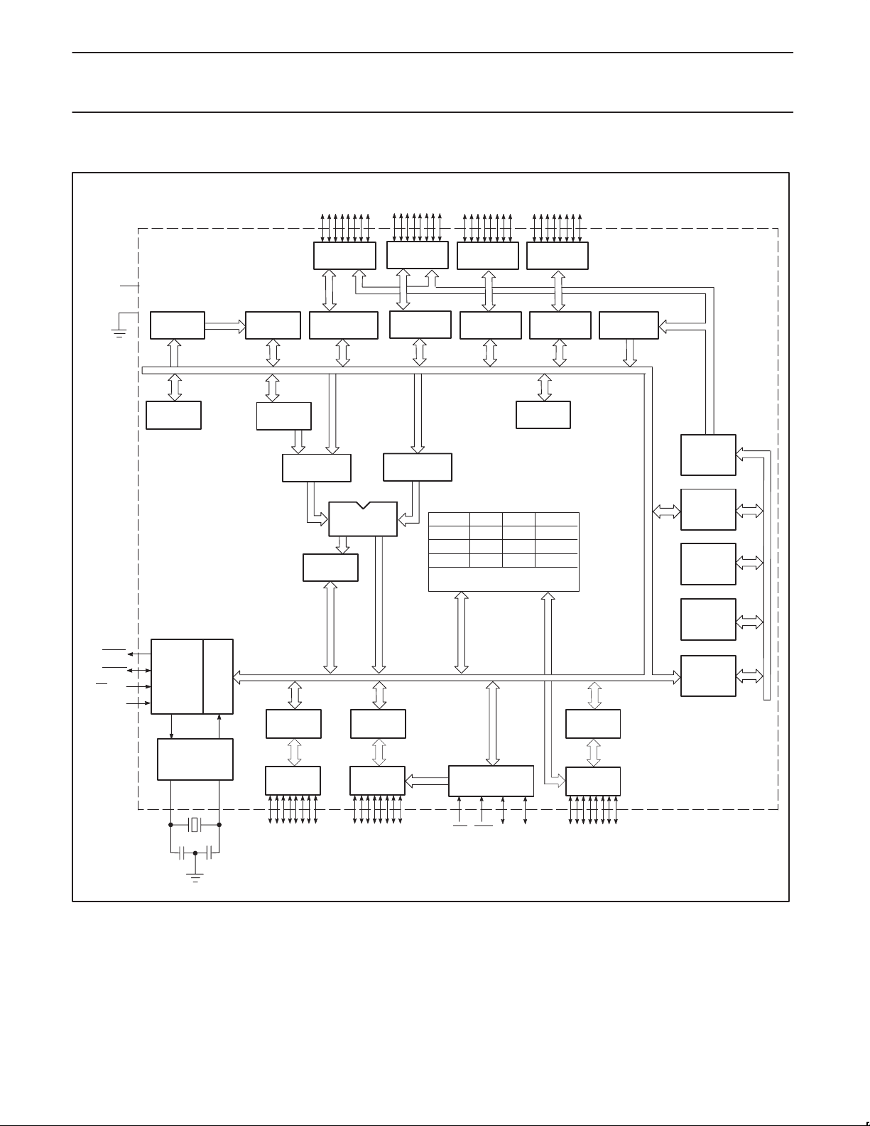
BLOCK DIAGRAM
P0.0–P0.7
PORT 0
DRIVERS
V
CC
V
SS
RAM ADDR
REGISTER
B
REGISTER
RAM
ACC
TMP2
PORT 0
LATCH
P2.0–P2.7
PORT 2
DRIVERS
PORT 2
LATCH
TMP1
P4.0–P4.7
PORT 4
DRIVERS
PORT 4
LATCH
80C451/83C451/87C451
P5.0–5.7
PORT 5
DRIVERS
PORT 5
LATCH
STACK
POINTER
4K x 8
ROM/EPROM
PROGRAM
ADDRESS
REGISTER
PSEN
ALE/PROG
EAV
PP
RST
TIMING
AND
CONTROL
OSCILLATOR
XTAL1 XTAL2
INSTRUCTION
PD
REGISTER
PORT 1
LATCH
PORT 1
DRIVERS
P1.0–P1.7
PSW
ALU
PORT 6
LATCH
PORT 6
DRIVERS
P6.0–P6.7
PCON SCON TMOD TCON
TH0 TL0 TH1
TL1
SBUF IE IP
INTERRUPT, SERIAL
PORT AND TIMER BLOCKS
PORT 6
CONTROL/STATUS
IDS ODS
AFLAG
BFLAG
PORT 3
LATCH
PORT 3
DRIVERS
P3.0–P3.7
BUFFER
PC
INCRE-
MENTER
PROGRAM
COUNTER
DPTR
SU00086
1998 May 01
3
Philips Semiconductors Product specification
80C51 8-bit microcontroller family
80C451/83C451/87C451
4K/128 OTP/ROM/ROMless, expanded I/O
ORDERING INFORMATION
ROMless ROM EPROM
1
TEMPERATURE RANGE °C
AND PACKAGE
SC80C451CCA68 SC83C451CCA68 SC87C451CCA68 OTP 0 to +70, Plastic Leaded Chip Carrier, 3.5 to 12 SOT188-3
SC80C451CGA68 SC83C451CGA68 SC87C451CGA68 OTP 0 to +70, Plastic Leaded Chip Carrier 3.5 to 16 SOT188-3
NOTE:
1. OTP = One Time Programmable
LOGIC SYMBOL
V
V
SS
CC
XTAL1
ADDRESS AND
DATA BUS
ADDRESS BUS
ALE/PROG
RxD
TxD
INT0
INT1
T0
T1
WR
RD
SECONDARY FUNCTIONS
EA
XTAL2
RST
/V
PSEN
PORT 3
PORT 0
PP
PORT 1PORT 2
FREQ
MHz
DRAWING
NUMBER
PORT 6 CONTROL
ODS
IDS
BFLAG
AFLAG
PORT 6
PORT 4
PORT 5
SU00085
1998 May 01
4
Philips Semiconductors Product specification
80C51 8-bit microcontroller family
80C451/83C451/87C451
4K/128 OTP/ROM/ROMless, expanded I/O
PIN DESCRIPTION
MNEMONIC
V
SS
V
CC
P0.0–0.7 17-10 I/O Port 0: Port 0 is an open-drain, bidirectional I/O port. Port 0 is also the multiplexed data and low-order
P1.0–P1.7 27-34 I/O Port 1: Port 1 is an 8-bit bidirectional I/O port with internal pull-ups. Port 1 receives the low-order
P2.0–P2.7 2-9 I/O Port 2: Port 2 is an 8-bit bidirectional I/O port with internal pull-ups. Port 2 emits the high-order address
P3.0–P3.7 36-43 I/O Port 3: Port 3 is an 8-bit bidirectional I/O port with internal pull-ups. Port 3 can sink/source three LS
P4.0–P4.7 26-19 I/O Port 4: Port 4 is a 8-bit (LCC) bidirectional I/O port with internal pull-ups. Port 4 can sink/source three
P5.0–P5.7 44-51 I/O Port 5: Port 5 is a 8-bit (LCC) bidirectional I/O port with internal pull-ups. Port 5 can sink/source three
P6.0–P6.7 59-66 I/O Port 6: Port 6 is a specialized 8-bit bidirectional I/O port with internal pull-ups. This special port can
ODS 55 I ODS: Output data strobe
IDS 56 I IDS: Input data strobe
BFLAG 57 I/O BFLAG: Bidirectional I/O pin with internal pull-ups
AFLAG 58 I/O AFLAG: Bidirectional I/O pin with internal pull-ups
RST 35 I Reset: A high on this pin for two machine cycles while the oscillator is running, resets the device. An
ALE/PROG 68 I/O Address Latch Enable/Program Pulse: Output pulse for latching the low byte of the address during
PSEN 67 O Program Store Enable: The read strobe to external program memory. PSEN is activated twice each
EA/V
PP
XTAL1 53 I Crystal 1: Input to the inverting oscillator amplifier that forms the oscillator. This input receives the
XTAL2 52 O Crystal 2: An output of the inverting amplifier that forms the oscillator. This pin should be floated when
PIN
NO.
TYPE NAME AND FUNCTION
54 I Ground: 0V reference.
18 I Power Supply: This is the power supply voltage for normal, idle, and power-down operation.
address bus during accesses to external memory. External pull-ups are required during program
verification. Port 0 can sink/source eight LS TTL inputs.
address bytes during program memory verification. Port 1 can sink/source three LS TTL inputs, and
drive CMOS inputs without external pull-ups.
bytes during access to external memory and receives the high-order address bits and control signals
during program verification. Port 2 can sink/source three LS TTL inputs, and drive CMOS inputs without
external pull-ups.
TTL inputs, and drive CMOS inputs without external pull-ups. Port 3 also serves the special functions
listed below:
36 I RxD (P3.0): Serial input port
37 O TxD (P3.1): Serial output port
38 I INT0 (P3.2): External interrupt
39 I INT1 (P3.3): External interrupt
40 I T0 (P3.4): Timer 0 external input
41 I T1 (P3.5): Timer 1 external input
42 O WR (P3.6): External data memory write strobe
43 O RD (P3.7): External data memory read strobe
LS TTL inputs and drive CMOS inputs without external pull-ups.
LS TTL inputs and drive CMOS inputs without external pull-ups.
sink/source three LS TTL inputs and drive CMOS inputs without external pull-ups. Port 6 can be used in
a strobed or non-strobed mode of operation. Port 6 works in conjunction with four control pins that
serve the functions listed below:
internal pull-down resistor permits a power-on reset using only an external capacitor connected to VCC.
an access to external memory. ALE is activated at a constant rate of 1/6 the oscillator frequency except
during an external data memory access, at which time one ALE is skipped. ALE can sink/source three
LS TTL inputs and drive CMOS inputs without external pull-ups. This pin is also the program pulse
during EPROM programming.
machine cycle during fetches from external program memory. However, when executing out of external
program memory, two activations of PSEN
memory. PSEN
eight LS TTL inputs and drive CMOS inputs without an external pull-up. This pin should be tied low
during programming.
1 I Instruction Execution Control/Programming Supply Voltage: When EA is held high, the CPU
executes out of internal program memory, unless the program counter exceeds 0FFFH. When EA is
held low, the CPU executes out of external program memory. EA
pin also receives the 12.75V programming supply voltage (V
external oscillator when an external oscillator is used.
an external oscillator is used.
is not activated during fetches from internal program memory. PSEN can sink/source
are skipped during each access to external program
must never be allowed to float. This
) during EPROM programming.
PP
1998 May 01
5

Philips Semiconductors Product specification
80C51 8-bit microcontroller family
4K/128 OTP/ROM/ROMless, expanded I/O
I/O Port Structure
The 8XC451 has a total of seven parallel I/O ports. The first four
ports, P0 through P3, are identical in function to those present on
the 80C51 family. The added ports 4 and 5 are identical in function
to port 1; that is, they are standard quasi-bidirectional ports with no
alternate functions and the standard output drive characteristics.
Port 6 is a specialized 8-bit bidirectional I/O port with internal
pullups.
Ports 4 and 5
Ports 4 and 5 are bidirectional I/O ports with internal pull-ups. Port 4
is an 8-bit port. Port 4 and port 5 pins with ones written to them, are
pulled high by the internal pull-ups, and in that state can be used as
inputs. Port 4 and 5 are addressed at the special function register
addresses shown in Table 1.
Port 6
Port 6 is a special 8-bit bidirectional I/O port with internal pull-ups
(see Figure 1). This special port can sink/source three LS TTL
inputs and drive CMOS inputs without external pullups. The flexibility
of this port facilitates high-speed parallel data communications. This
port can be used as a standard I/O port, or in strobed modes of
operation in conjunction with four special control lines: ODS
AFLAG, and BFLAG. Port 6 operating modes are controlled by the
port 6 control status register (CSR). Port 6 and the CSR are
addressed at the special function register addresses shown in Table
1. The following four control pins are used in conjunction with port 6:
ODS
– Output data strobe (Active Low) for port 6. ODS can be
programmed to control the port 6 output drivers and the output
buffer full flag (OBF), or to clear only the OBF flag bit in the CSR
(output-always mode). ODS
the OBF flag can be programmed to be cleared on the negative or
positive edge of ODS
IDS – Input data strobe (Active Low) for port 6. IDS is used to
control the port 6 input latch and input buffer full flag (IBF) bit in the
CSR. The input data latch can be programmed to be transparent
when IDS
latch only on the positive transition of IDS
flag is set on the negative or positive transition of IDS
BFLAG – BFLAG is a bidirectional I/O pin which can be
programmed to be an output, set high or low under program control,
or to output the state of the input buffer full flag. BFLAG can also be
programmed to input an enable signal for port 6. When BFLAG is
used as an enable input, port 6 output drivers are in the
high-impedance state, and the input latch does not respond to the
IDS
BFLAG is low. This feature facilitates the use of the SC8XC451 in
bused multiprocessor systems.
AFLAG – AFLAG is a bidirectional I/O pin which can be
programmed to be an output set high or low under program control,
or to output the state of the output buffer full flag. AFLAG can also
be programmed to be an input which selects whether the contents of
the output buffer, or the contents of the port 6 control status register
will output on port 6. This feature grants complete port 6 status to
external devices.
Port 6 can be used in a number of different ways to facilitate data
communication. It can be used as a processor bus interface, as a
standard quasi-bidirectional I/O port, or as a parallel printer port
(either polled or interrupt driven).
is low and latched on the positive transition of IDS, or to
strobe when BFLAG is high. Both features are enabled when
is active low for output driver control.
.
. Correspondingly , the IBF
, IDS,
.
80C451/83C451/87C451
Processor Bus Interface
Port 6 allows the use of an 8XC451 as an element on a
microprocessor type bus. The host processor could be a general
purpose MPU or the data bus of a microcontroller like the 8XC451
itself. Setting up the 8XC451 as a processor bus interface allows
single or multiple microcontrollers to be used on a bus as flexible
peripheral processing elements. Applications can include: keyboard
scanners, serial I/O controllers, servo controllers, etc.
On reset, port 6 is programmed correctly (that is, Special Function
registers CSR and P6) for use as a bus interface. This prevents the
interface from disrupting data on the bus of a host processor during
power-up.
Standard Quasi-bidirectional I/O Port
To use port 6 as a common I/O port, all of the control pins should be
tied to ground. On hardware reset, bits 2-7 of the CSR are set to
one. With the control pins grounded, the port’s operation and
electrical characteristics will be identical to port 1 on the 80C51. No
further software initialization is required.
Parallel Printer Port
The 8XC451 has the capacity to permit all of the intelligent features
of a common printer to be handled by a single chip. The features of
port 6 allow a parallel port to be designed with only line driving and
receiving chips required as additional hardware. The onboard UART
allows RS232 interfacing with only level shifting chips added. The
8-bit parallel ports 0 to 6 are ample to drive onboard control
functions, even when ports are used for external memory access,
interrupts, and other functions. The RAM addressing ability of ports
0 to 2 can be used to address up to 64k bytes of a hardware
buffer/spooler.
In addition, either end of a parallel interface can be implemented
using port 6, and the interfaces can be interrupt driven or polled in
either case. For more detailed information on port 6 usage, refer to
the application notes entitled “80C451 Operation of Port 6” and
“256k Centronics Printer Buffer Using the SC87C451
Microcontroller.”
CONTROL STATUS REGISTER
The control status register (CSR) establishes the mode of operation
for port 6 and indicates the current status of port 6 I/O registers. All
control status register bits can be read and written by the CPU,
except bits 0 and 1, which are read only. Reset writes ones to bits 2
through 7, and writes zeros to bits 0 and 1 (see Table 3).
CSR.0 Input Buffer Full Flag (IBF) (Read Only) – The IBF bit is
set to a logic 1 when port 6 data is loaded into the input buffer under
control of IDS
IDS
, as determined by CSR.2 IBF is cleared when the CPU reads
the input buffer register.
CSR.1 Output Buffer Full Flag (OBF) (Read Only) – The OBF flag
is set to a logic 1 when the CPU writes to the port 6 output data
buffer . OBF is cleared by the positive or negative edge of ODS
determined by CSR.3.
CSR.2 IDS Mode Select (IDSM) – When CSR.2 = 0, a low-to-high
transition on the IDS
loaded on the IDS
transition on the IDS
transparent when IDS
. This can occur on the negative or positive edge of
, as
pin sets the IBF flag. The Port 6 input buffer is
positive edge. When CSR.2 = 1, a high-to-low
pin sets the IBF flag. Port 6 input buffer is
is low, and latched when IDS is high.
1998 May 01
6

Philips Semiconductors Product specification
80C51 8-bit microcontroller family
80C451/83C451/87C451
4K/128 OTP/ROM/ROMless, expanded I/O
CSR.3 Output Buffer Full Flag Clear Mode (OBFC) – When
CSR.3 = 1, the positive edge of the ODS
When CSR.3 = 0, the negative edge of the ODS
input clears the OBF flag.
input clears the
OBF flag.
CSR.4, CSR.5 AFLAG Mode Select
(MA0, MA1) – Bits 4 and 5 select the mode of operation for the
AFLAG pin as follows:
MA1 MA0 AFLAG Function
0 0 Logic 0 output
0 1 Logic 1 output
1 0 OBF flag output (CSR.1)
1 1 Select (SEL) input mode
The select (SEL) input mode is used to determine whether the port 6
data register or the control status register is output on port 6. When
the select feature is enabled, the AFLAG input controls the source of
port 6 output data. A logic 0 on AFLAG input selects the port 6 data
register, and a logic 1 on AFLAG input selects the control status
register.
Table 1. Special Function Register Addresses
REGISTER ADDRESS BIT ADDRESS
NAME SYMBOL ADDRESS MSB LSB
Port 4 P4 C0 C7 C6 C5 C4 C3 C2 C1 C0
Port 5 P5 C8 CF CE CD CC CB CA C9 C8
Port 6 data P6 D8 DF DE DD DC DB DA D9 D8
Port 6 control status CSR E8 EF EE ED EC EB EA E9 E8
CSR.6, CSR.7 BFLAG Mode Select
(MB0, MB1) – Bits 6 and 7 select the mode operation as follows:
MB1 MB0 BFLAG Function
0 0 Logic 0 output
0 1 Logic 1 output
1 0 IBF flag output (CSR.0)
1 1 Port enable (PE
In the port enable mode, IDS
)
and ODS inputs are disabled when
BFLAG input is high. When the BFLAG input is low, the port is
enabled for I/O.
SPECIAL FUNCTION REGISTER ADDRESSES
The SFRs are identical to those of the standard 80C51 with the
exception of four registers that have been added to allow control of
the three additional I/O ports P4, P5, and P6. The additional
registers are P4, P5, P6, and CSR. Registers P4, P5, and P6
function as port latches for ports 4, 5, and 6, respectively. These
registers operate identically to those for ports 0 through 3 of the
80C51.
AFLAG
MODE
(CSR.4/.5)
OUTPUT BUFFER
FULL (CSR.1)
ODSBFLAGAFLAG
BFLAG/ODS
MODE
(CSR.6/.7)
INPUT BUFFER
FULL (CSR.0)
CONTROL/STATUS
REGISTER (CSR)
PORT 6
OUTPUT
DRIVERS
MUX
OUTPUT BUFFER
(P6 WRITE)
INTERNAL BUS
INPUT
BUFFER
(P6 READ)
Figure 1. Port 6 Block Diagram
IDS
IDS
MODE
EDGE/LEVEL
SELECT (CSR.2)
SU00087
1998 May 01
7
 Loading...