

Philips 74HCT4511U, 74HCT4511N, 74HCT4511D, 74HC4511U, 74HC4511N Datasheet
...
DATA SH EET
Product specification
File under Integrated Circuits, IC06
December 1990
INTEGRATED CIRCUITS
74HC/HCT4511
BCD to 7-segment
latch/decoder/driver
For a complete data sheet, please also download:
•The IC06 74HC/HCT/HCU/HCMOS Logic Family Specifications
•The IC06 74HC/HCT/HCU/HCMOS Logic Package Information
•The IC06 74HC/HCT/HCU/HCMOS Logic Package Outlines
December 1990 2
Philips Semiconductors Product specification
BCD to 7-segment latch/decoder/driver 74HC/HCT4511
FEATURES
• Latch storage of BCD inputs
• Blanking input
• Lamp test input
• Driving common cathode LED displays
• Guaranteed 10 mA drive capability per output
• Output capability: non-standard
• ICC category: MSI
GENERAL DESCRIPTION
The 74HC/HCT4511 are high-speed Si-gate CMOS
devices and are pin compatible with “4511” of the “4000B”
series. They are specified in compliance with JEDEC
standard no. 7A.
The 74HC/HCT4511 are BCD to 7-segment
latch/decoder/drivers with four address inputs (D
1
to D4),
an active LOW latch enable input (LE), an active LOW
ripple blanking input (BI), an active LOW lamp test input
(LT), and seven active HIGH segment outputs (Qa to Qg).
When LE is LOW, the state of the segment outputs (Qa to
Qg) is determined by the data on D1 to D4.
When LE goes HIGH, the last data present on D1 to D4 are
stored in the latches and the segment outputs remain
stable.
When LT is LOW, all the segment outputs are HIGH
independent of all other input conditions. With LT HIGH, a
LOW onBI forces all segment outputs LOW. The inputsLT
and BI do not affect the latch circuit.
APPLICATIONS
• Driving LED displays
• Driving incandescent displays
• Driving fluorescent displays
• Driving LCD displays
• Driving gas discharge displays
QUICK REFERENCE DATA
GND = 0 V; T
amb
=25°C; tr=tf= 6 ns
Notes
1. C
PD
is used to determine the dynamic power dissipation (PD in µW):
PD=CPD× V
CC
2
× fi+∑(CL× V
CC
2
× fo) where:
fi= input frequency in MHz
fo= output frequency in MHz
∑ (CL× V
CC
2
× fo) = sum of outputs
CL= output load capacitance in pF
VCC= supply voltage in V
2. For HC the condition is VI= GND to V
CC
For HCT the condition is VI= GND to VCC− 1.5 V
SYMBOL PARAMETER CONDITIONS
TYPICAL
UNIT
HC HCT
t
PHL
/ t
PLH
propagation delay CL= 15 pF; VCC=5 V
D
n
to Q
n
24 24 ns
LE to Q
n
23 24 ns
BI to Q
n
19 20 ns
LT to Q
n
12 13 ns
C
I
input capacitance 3.5 3.5 pF
C
PD
power dissipation capacitance per latch notes 1 and 2 64 64 pF
December 1990 3
Philips Semiconductors Product specification
BCD to 7-segment latch/decoder/driver 74HC/HCT4511
ORDERING INFORMATION
See
“74HC/HCT/HCU/HCMOS Logic Package Information”
.
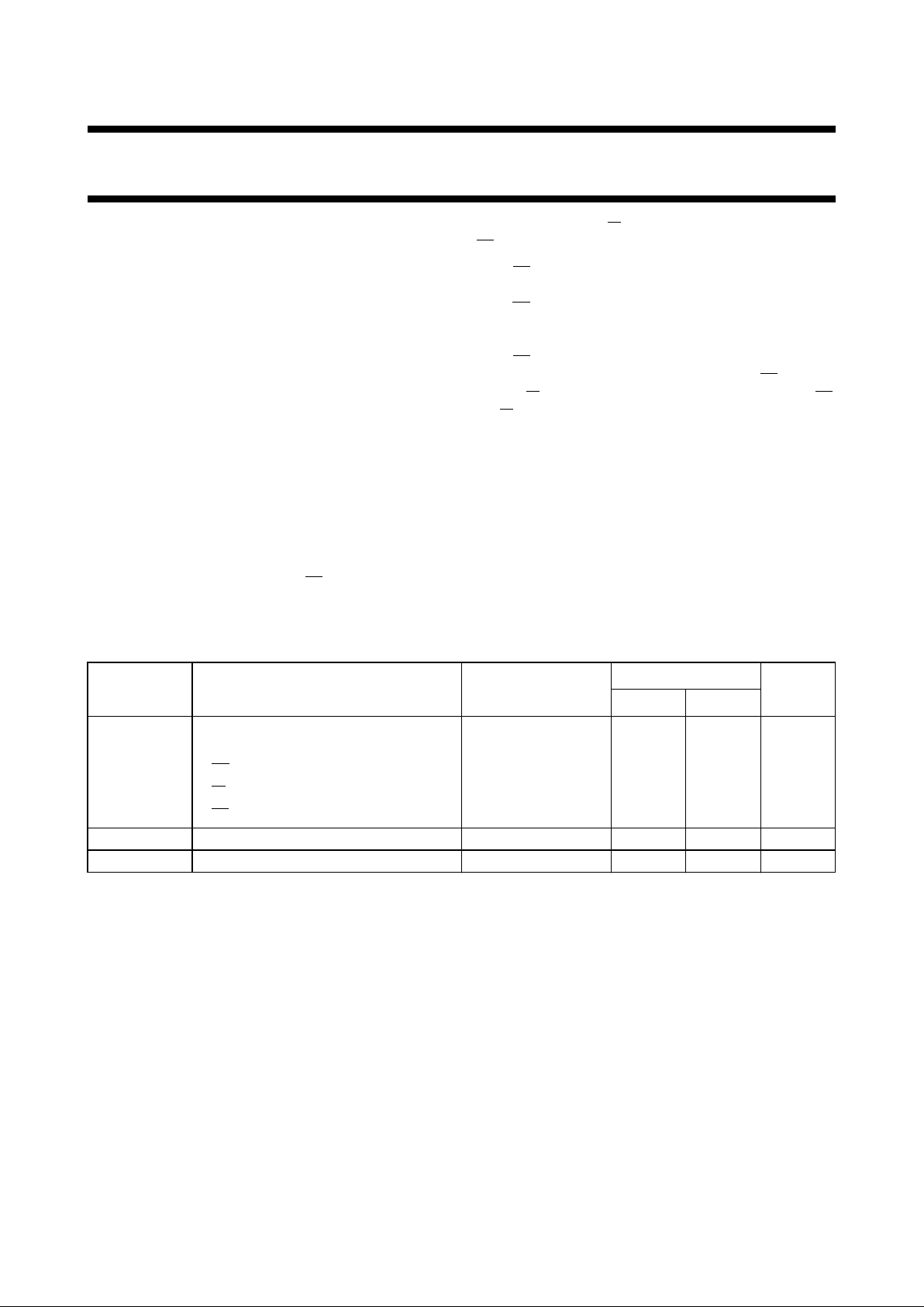
PIN DESCRIPTION
PIN NO. SYMBOL NAME AND FUNCTION
3
LT lamp test input (active LOW)
4
BI ripple blanking input (active LOW)
5
LE latch enable input (active LOW)
7, 1, 2, 6 D
1
to D
4
BCD address inputs
8 GND ground (0 V)
13, 12, 11, 10, 9, 15, 14 Q
a
to Q
g
segments outputs
16 V
CC
positive supply voltage
Fig.1 Pin configuration. Fig.2 Logic symbol. Fig.3 IEC logic symbol.
December 1990 4
Philips Semiconductors Product specification
BCD to 7-segment latch/decoder/driver 74HC/HCT4511
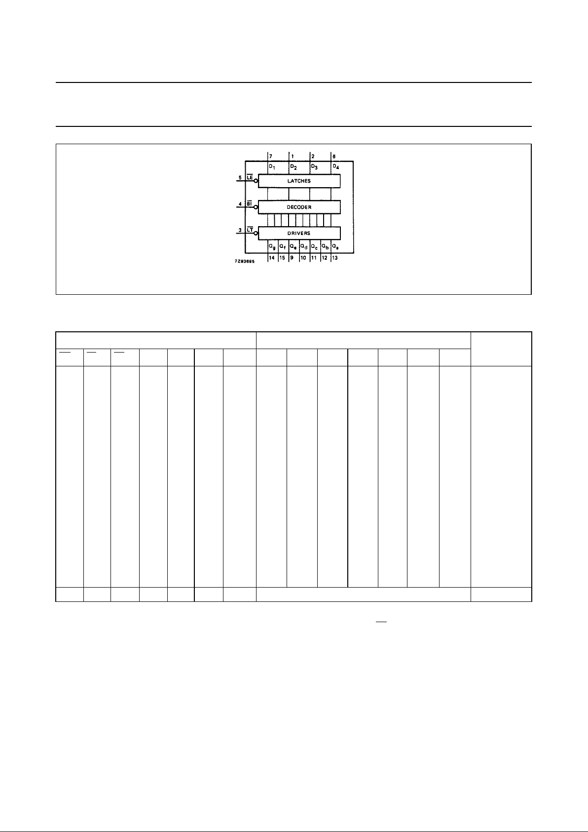
FUNCTION TABLE
Note
1. Depends upon the BCD-code applied during the LOW-to-HIGH transition of
LE.
H = HIGH voltage level
L = LOW voltage level
X = don’t care
INPUTS OUTPUTS
DISPLAY
LE BI LTD4D3D2D1QaQbQcQdQeQfQ
g
XXLXXXX HHHHHH H8
XLHXXXX LLLLLLLblank
L
L
L
L
H
H
H
H
H
H
H
H
L
L
L
L
L
L
L
L
L
L
H
H
L
H
L
H
H
L
H
H
H
H
H
H
H
H
L
H
H
L
H
H
H
L
H
L
H
L
L
L
L
L
H
H
0
1
2
3
L
L
L
L
H
H
H
H
H
H
H
H
L
L
L
L
H
H
H
H
L
L
H
H
L
H
L
H
L
H
L
H
H
L
L
H
H
H
H
H
L
H
H
L
L
L
H
L
H
H
H
L
H
H
H
L
4
5
6
7
L
L
L
L
H
H
H
H
H
H
H
H
H
H
H
H
L
L
L
L
L
L
H
H
L
H
L
H
H
H
L
L
H
H
L
L
H
H
L
L
H
L
L
L
H
L
L
L
H
H
L
L
H
H
L
L
8
9
blank
blank
L
L
L
L
H
H
H
H
H
H
H
H
H
H
H
H
H
H
H
H
L
L
H
H
L
H
L
H
L
L
L
L
L
L
L
L
L
L
L
L
L
L
L
L
L
L
L
L
L
L
L
L
L
L
L
L
blank
blank
blank
blank
HHHXXXX
(1) (1)
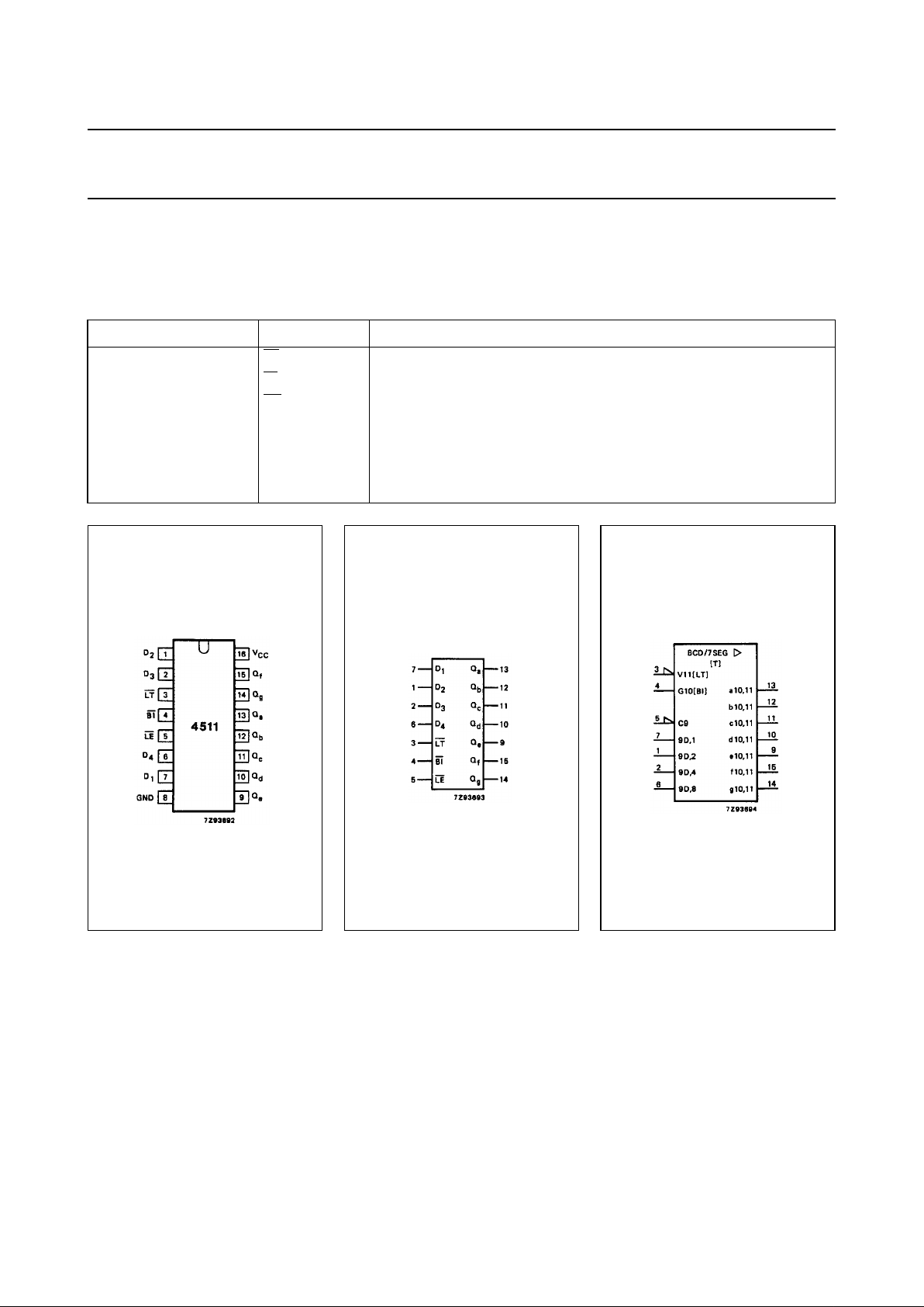
Fig.4 Functional diagram.
 Loading...