

Philips 74HCT393DB, 74HCT393D, 74HCT393U, 74HCT393PW, 74HCT393NB Datasheet
...
DATA SH EET
Product specification
File under Integrated Circuits, IC06
December 1990
INTEGRATED CIRCUITS
74HC/HCT393
Dual 4-bit binary ripple counter
For a complete data sheet, please also download:
•The IC06 74HC/HCT/HCU/HCMOS Logic Family Specifications
•The IC06 74HC/HCT/HCU/HCMOS Logic Package Information
•The IC06 74HC/HCT/HCU/HCMOS Logic Package Outlines
December 1990 2
Philips Semiconductors Product specification
Dual 4-bit binary ripple counter 74HC/HCT393
FEATURES
• Two 4-bit binary counters with individual clocks
• Divide-by any binary module up to 28 in one package
• Two master resets to clear each 4-bit counter
individually
• Output capability: standard
• ICC category: MSI
GENERAL DESCRIPTION
The 74HC/HCT393 are high-speed Si-gate CMOS devices
and are pin compatible with low power Schottky TTL
(LSTTL). They are specified in compliance with JEDEC
standard no. 7A.
The 74HC/HCT393 are 4-bit binary ripple counters with
separate clocks (1
CP and 2 CP) and master reset (1MR
and 2MR) inputs to each counter. The operation of each
half of the “393” is the same as the “93” except no external
clock connections are required.
The counters are triggered by a HIGH-to-LOW transition of
the clock inputs. The counter outputs are internally
connected to provide clock inputs to succeeding stages.
The outputs of the ripple counter do not change
synchronously and should not be used for high-speed
address decoding.
The master resets are active-HIGH asynchronous inputs
to each 4-bit counter identified by the “1” and “2” in the pin
description.
A HIGH level on the nMR input overrides the clock and
sets the outputs LOW.
QUICK REFERENCE DATA
GND = 0 V; T
amb
= 25 °C; tr= tf= 6 ns
Notes
1. C
PD
is used to determine the dynamic power dissipation (PDin µW):
PD= CPD× V
CC
2
× fi+∑(CL× V
CC
2
× fo) where:
fi= input frequency in MHz
fo= output frequency in MHz
∑ (CL× V
CC
2
× fo) = sum of outputs
CL= output load capacitance in pF
VCC= supply voltage in V
2. For HC the condition is VI= GND to V
CC
For HCT the condition is VI= GND to VCC− 1.5 V
ORDERING INFORMATION
See
“74HC/HCT/HCU/HCMOS Logic Package Information”
.
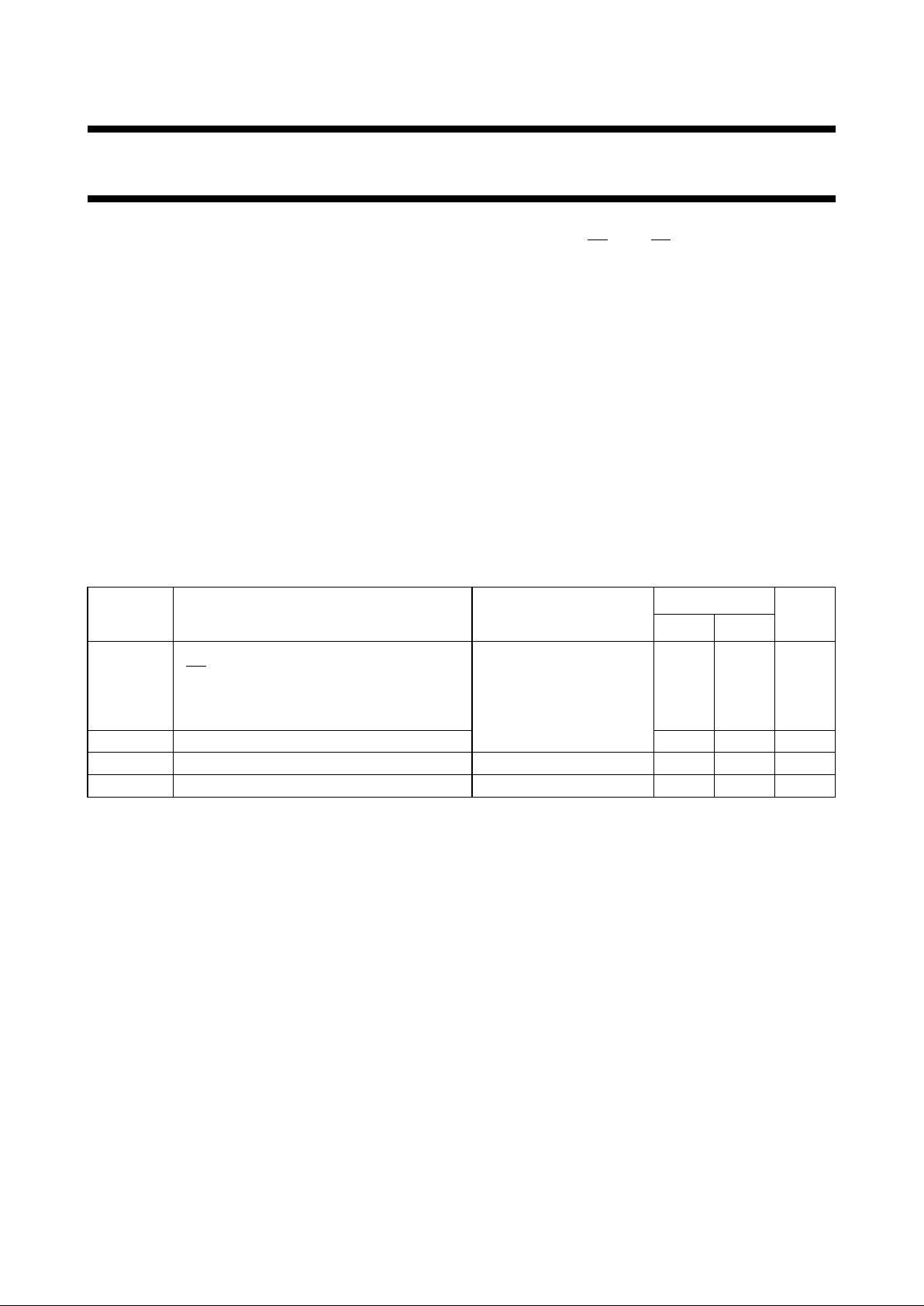
SYMBOL PARAMETER CONDITIONS
TYPICAL
UNIT
HC HCT
t
PHL
/ t
PLH
propagation delay CL= 15 pF; VCC= 5 V
n
CP to nQ
0
12 20 ns
nQ to nQ
n+1
56ns
nMR to nQ
n
11 15 ns
f
max
maximum clock frequency 99 53 MHz
C
I
input capacitance 3.5 3.5 pF
C
PD
power dissipation capacitance per counter notes 1 and 2 23 25 pF
December 1990 3
Philips Semiconductors Product specification
Dual 4-bit binary ripple counter 74HC/HCT393
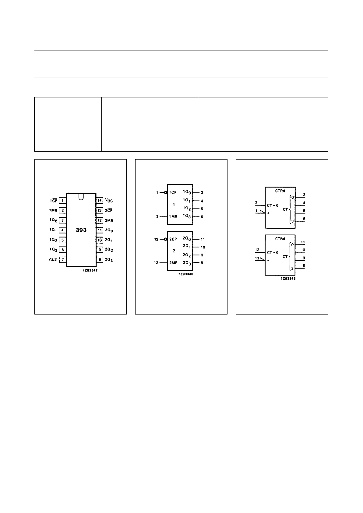
PIN DESCRIPTION
PIN NO. SYMBOL NAME AND FUNCTION
1, 13 1
CP, 2CP clock inputs (HIGH-to-LOW, edge-triggered)
2, 12 1MR, 2MR asynchronous master reset inputs (active HIGH)
3, 4, 5, 6, 11, 10, 9, 8 1Q
0
to 1Q3, 2Q0to 2Q
3
flip-flop outputs
7 GND ground (0 V)
14 V
CC
positive supply voltage
Fig.1 Pin configuration. Fig.2 Logic symbol. Fig.3 IEC logic symbol.
 Loading...