

Philips 74HCT390U, 74HCT390N, 74HCT390DB, 74HCT390D, 74HC390U Datasheet
...
DATA SH EET
Product specification
File under Integrated Circuits, IC06
December 1990
INTEGRATED CIRCUITS
74HC/HCT390
Dual decade ripple counter
For a complete data sheet, please also download:
•The IC06 74HC/HCT/HCU/HCMOS Logic Family Specifications
•The IC06 74HC/HCT/HCU/HCMOS Logic Package Information
•The IC06 74HC/HCT/HCU/HCMOS Logic Package Outlines
December 1990 2
Philips Semiconductors Product specification
Dual decade ripple counter 74HC/HCT390
FEATURES
• Two BCD decade or bi-quinary counters
• One package can be configured to divide-by-2, 4, 5, 10,
20, 25, 50 or 100
• Two master reset inputs to clear each decade counter
individually
• Output capability: standard
• ICC category: MSI
GENERAL DESCRIPTION
The 74HC/HCT390 are high-speed Si-gate CMOS devices
and are pin compatible with low power Schottky TTL
(LSTTL). They are specified in compliance with JEDEC
standard no. 7A.
The 74HC/HCT390 are dual 4-bit decade ripple counters
divided into four separately clocked sections. The counters
have two divide-by-2 sections and two divide-by-5
sections. These sections are normally used in a BCD
decade or bi-quinary configuration, since they share a
common master reset input (nMR). If the two master reset
inputs (1MR and 2MR) are used to simultaneously clear all
8 bits of the counter, a number of counting configurations
are possible within one package. The separate clocks
(n
CP0and nCP1) of each section allow ripple counter or
frequency division applications of divide-by-2, 4, 5, 10, 20,
25, 50 or 100.
Each section is triggered by the HIGH-to-LOW transition of
the clock inputs (nCP0and nCP1). For BCD decade
operation, the nQ0output is connected to the nCP1 input
of, the divide-by-5 section. For bi-quinary decade
operation, the nQ3 output is connected to the nCP0input
and nQ0becomes the decade output.
The master reset inputs (1MR and 2MR) are active HIGH
asynchronous inputs to each decade counter which
operates on the portion of the counter identified by the “1”
and “2” prefixes in the pin configuration. A HIGH level on
the nMR input overrides the clocks and sets the four
outputs LOW.
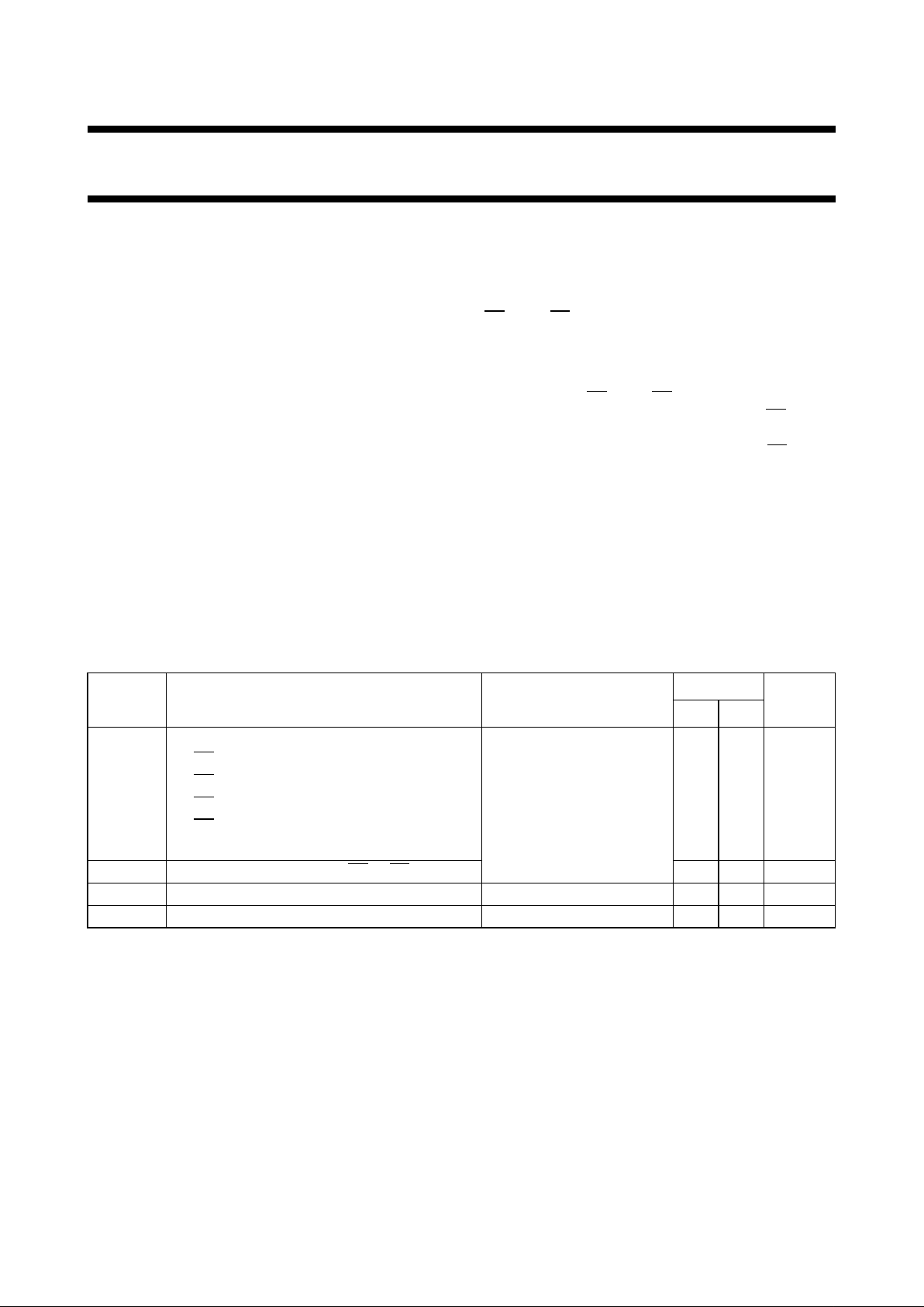
QUICK REFERENCE DATA
GND = 0 V; T
amb
=25°C; tr=tf= 6 ns
Notes
1. C
PD
is used to determine the dynamic power dissipation (PD in µW):
PD=CPD× V
CC
2
× fi+∑ (CL× V
CC
2
× fo) where:
fi= input frequency in MHz
fo= output frequency in MHz
∑ (CL× V
CC
2
× fo) = sum of outputs
CL= output load capacitance in pF
VCC= supply voltage in V
2. For HC the condition is VI= GND to V
CC
For HCT the condition is VI= GND to VCC−1.5 V
SYMBOL PARAMETER CONDITIONS
TYPICAL
UNIT
HC HCT
t
PHL
/ t
PLH
propagation delay CL= 15 pF; VCC=5V
n
CP0 to nQ
0
14 18 ns
n
CP1 to nQ
1
15 19 ns
n
CP1to nQ
2
23 26 ns
n
CP1to nQ
3
15 19 ns
nMR to Q
n
16 18 ns
f
max
maximum clock frequency nCP0,nCP
1
66 61 MHz
C
I
input capacitance 3.5 3.5 pF
C
PD
power dissipation capacitance per counter notes 1 and 2 20 21 pF
December 1990 3
Philips Semiconductors Product specification
Dual decade ripple counter 74HC/HCT390
ORDERING INFORMATION
See
“74HC/HCT/HCU/HCMOS Logic Package Information”
.
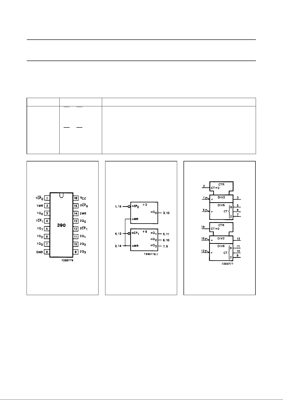
PIN DESCRIPTION
PIN NO. SYMBOL NAME AND FUNCTION
1, 15 1
CP0, 2CP
0
clock input divide-by-2 section (HIGH-to-LOW, edge-triggered)
2, 14 1MR, 2MR asynchronous master reset inputs (active HIGH)
3, 5, 6, 7 1Q
0
to 1Q
3
flip-flop outputs
4, 12 1
CP1, 2CP
1
clock input divide-by-5 section (HIGH-to-LOW, edge triggered)
8 GND ground (0 V)
13, 11, 10, 9 2Q
0
to 2Q
3
flip-flop outputs
16 V
CC
positive supply voltage
Fig.1 Pin configuration. Fig.2 Logic symbol. Fig.3 IEC logic symbol.
 Loading...