

Philips 74abt5074 DATASHEETS
Philips Semiconductors Advanced BiCMOS Products Product specification
74ABT5074
Synchronizing dual D-type flip-flop
with metastable immune characteristics
1
December 15, 1994 853-1775 14470
FEATURES
•Metastable immune characteristics
•Pin compatible with 74F74 and 74F5074
•Typical f
MAX
= 200MHz
•Output skew guaranteed less than 2.0ns
•High source current (I
OH
= 15mA) ideal for clock driver
applications
•Output capability: +20mA/–15mA
•Latch-up protection exceeds 500mA per Jedec JC40.2 Std 17
•ESD protection exceeds 2000V per MIL STD 883 Method 3015
and 200V per Machine Model
DESCRIPTION
The 74ABT5074 is a dual positive edge-triggered D-type flip-flop
featuring individual data, clock, set and reset inputs; also true and
complementary outputs.
Set (S
Dn) and reset (RDn) are asynchronous active low inputs and
operate independently of the clock (CPn) input. Data must be stable
just one setup time prior to the low-to-high transition of the clock for
guaranteed propagation delays.
Clock triggering occurs at a voltage level and is not directly related
to the transition time of the positive-going pulse. Following the hold
time interval, data at the Dn input may be changed without affecting
the levels of the output.
The 74ABT5074 is designed so that the outputs can never display a
metastable state due to setup and hold time violations. If setup time
and hold time are violated the propagation delays may be extended
beyond the specifications but the outputs will not glitch or display a
metastable state. Typical metastability parameters for the
74ABT5074 are:
τ ≅ 94ps and T
o
≅ 1.3 × 10
7
sec
where τ represents a function of the rate at which a latch in a
metastable state resolves that condition and T
0
represents a
function of the measurement of the propensity of a latch to enter a
metastable state.
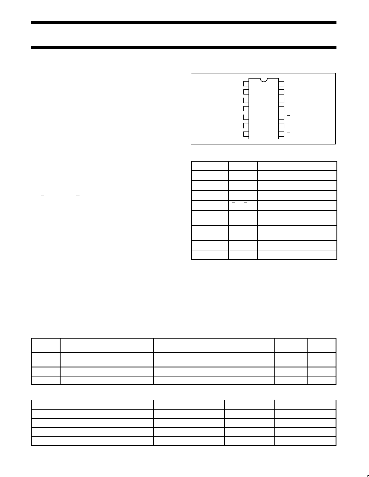
PIN CONFIGURATION
14
13
12
11
10
9
87
6
5
4
3
2
1
GND
V
CC
SD1
Q1
Q1
CP1
R
D1
D1
R
D0
D0
Q
0
CP0
SD0
Q0
SA00001
PIN DESCRIPTION
PIN NUMBER SYMBOL NAME AND FUNCTION
2, 12 D0, D1 Data inputs
3, 11 CP0, CP1 Clock inputs (active rising edge)
4, 10 SD0, SD1 Set inputs (active-Low)
1, 13 RD0, RD1 Reset inputs (active-Low)
5, 9 Q0, Q1
Data outputs (active-Low),
non-inverting
6, 8 Q0, Q1
Data outputs (active-Low),
inverting
7 GND Ground (0V)
14 V
CC
Positive supply voltage
QUICK REFERENCE DATA
SYMBOL PARAMETER
CONDITIONS
T
amb
= 25°C; GND = 0V
TYPICAL UNIT
t
PLH
t
PHL
Propagation delay
CPn to Qn or Qn
CL = 50pF; VCC = 5V
2.8
2.4
ns
C
IN
Input capacitance VI = 0V or V
CC
3 pF
I
CC
Total supply current Outputs disabled; VCC =5.5V 2 µA
ORDERING INFORMATION
PACKAGES TEMPERATURE RANGE ORDER CODE DRAWING NUMBER
14-pin plastic DIP –40°C to +85°C 74ABT5074N SOT27-1
14-pin plastic SOL –40°C to +85°C 74ABT5074D SOT108-1
14-pin plastic shrink small outline SSOP Type II –40°C to +85°C 74ABT5074DB SOT337-1
14-pin plastic thin shrink small outline (TSSOP) Type I –40°C to +85°C 74ABT5074PW SOT402-1
Philips Semiconductors Advanced BiCMOS Products Product specification
74ABT5074
Synchronizing dual D-type flip-flop
with metastable immune characteristics
December 15, 1994
2
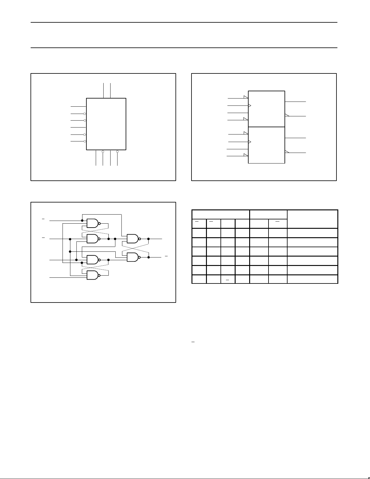
LOGIC SYMBOL
Q0 Q0 Q1 Q1
5 6 9 8
VCC = Pin 14
GND = Pin 7
3
4
1
11
10
13
CP0
SD0
RD0
CP1
SD1
RD1
D0 D1
2 12
SA00002
IEC/IEEE SYMBOL
4
3
2
1
10
11
12
13
5
6
9
8
S
S
C1
C2
R
1D
2D
R
SA00003
LOGIC DIAGRAM
VCC = Pin 14
GND = Pin 7
5, 9
6, 8
Q
Q
4, 10
1, 13
3, 11
2, 12
S
D
R
D
CP
D
SF00048
FUNCTION TABLE
INPUTS OUTPUTS
OPERATING
SD RD CP D Q Q
L H X X H L Asynchronous set
H L X X L H Asynchronous reset
L L X X L H Undetermined*
H H ↑ h H L Load ”1”
H H ↑ l L H Load ”0”
H H ↑ X NC NC Hold
NOTES:
H = High voltage level
h = High voltage level one setup time prior to low-to-high clock
transition
L = Low voltage level
l = Low voltage level one setup time prior to low-to-high clock
transition
NC= No change from the previous setup
X = Don’t care
↑ = Low-to-high clock transition
↑
= Not low-to-high clock transition
* = This setup is unstable and will change when either set or
reset return to the high level
MODE
Philips Semiconductors Advanced BiCMOS Products Product specification
74ABT5074
Synchronizing dual D-type flip-flop
with metastable immune characteristics
December 15, 1994
3
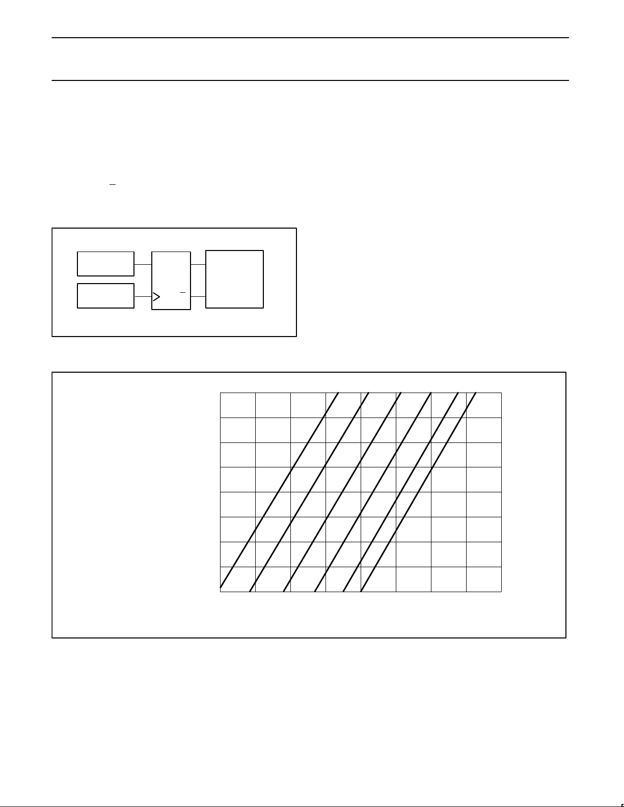
METASTABLE IMMUNE CHARACTERISTICS
Philips Semiconductors uses the term ‘metastable immune’ to
describe characteristics of some of the products in its family. By
running two independent signal generators (see Figure 1) at nearly
the same frequency (in this case 10MHz clock and 10.02MHz data)
the device-under-test can often be driven into a metastable state. If
the Q output is then used to trigger a digital scope set to infinite
persistence the Q
output will build a waveform. An experiment was
run by continuously operating the devices in the region where
metastability will occur.
D Q
Q
CP
TRIGGER
DIGITAL
SCOPE
INPUT
SIGNAL
GENERATOR
SA00004
SIGNAL
GENERATOR
E6 E8 E10 E12 E14 E15 = fc*fi
E13
E12
E11
E10
E9
E8
E7
E6
E5
10,000 YEARS
100 YEARS
ONE YEAR
ONE WEEK
MTBF
(SECONDS)
t’ (NANOSECONDS)
4 5 6 7 8
MTBF = e
(t’/τ)
/TO*fC*f
I
SA00005
VCC = 5V, T
amb
= 25°C, τ =94ps, To = 1.3x10⁷ sec
Figure 1. Test Setup
After determining the T
between failures (MTBF) is simple. Suppose a designer wants to
use the 74ABT5074 for synchronizing asynchronous data that is
arriving at 10MHz (as measured by a frequency counter), has a
clock frequency of 50MHz, and has decided that he would like to
sample the output of the 74ABT5074 7 nanoseconds after the clock
edge. He simply plugs his number into the following equation:
MTBF = e
In this formula, fC is the frequency of the clock, fI is the average
input event frequency, and t’ is the time after the clock pulse that the
output is sampled (t’ > h, h being the normal propagation delay). In
this situation the f
because input events consist of both of low and high transitions.
Multiplying f
by fC gives an answer of 10
I
clear that the MTBF is greater than 10
formula the actual MTBF is 1.69 × 10
and τ of the flop, calculating the mean time
0
(t’/τ)
/ TO*fC*f
I
will be twice the data frequency of 20 MHz
I
15
Hz2. From Figure 2 it is
10
seconds. Using the above
10
seconds or about 535 years.
Figure 2. Mean Time Between Failures (MTBF) versus t’
 Loading...