

Philips 74ABT2244PW, 74ABT2244N, 74ABT2244DB, 74ABT2244D Datasheet

INTEGRATED CIRCUITS
74ABT2244
Octal buffer/line driver with 30Ω series
termination resistors (3-State)
Product specification
Supersedes data of 1996 Oct 23
IC23 Data Handbook
1998 Jan 16

Philips Semiconductors Product specification
Octal buffer/line driver with 30Ω series
termination resistors (3-State)
FEA TURES
•Octal bus interface
•3-State buffers
•Live insertion/extraction permitted
•Outputs include series resistance of 30Ω, making external
termination resistors unnecessary
•Output capability: +5mA/–32mA
•Latch-up protection exceeds 500mA per Jedec Std 17
•ESD protection exceeds 2000 V per MIL STD 883 Method 3015
and 200 V per Machine Model
•Power-up 3-State
•Same part as 74ABT244-1
•Inputs are disabled during 3-State mode
QUICK REFERENCE DATA
SYMBOL PARAMETER
C
t
PLH
t
PHL
C
OUT
I
CCZ
IN
Propagation delay
An to Yn
CL = 50pF; VCC = 5V
Input capacitance VI = 0V or V
Output capacitance Outputs disabled; VO = 0V or V
Total supply current Outputs disabled; VCC = 5.5V 50 µA
74ABT2244
DESCRIPTION
The 74ABT2244 high-performance BiCMOS device combines low
static and dynamic power dissipation with high speed.
The 74ABT2244 device is an octal buffer that is ideal for driving bus
lines. The device features two Output Enables (1OE
controlling four of the 3-State outputs.
The 74ABT2244 is designed with 30Ω series resistance in both the
High and Low states of the output. This design reduces line noise in
applications such as memory address drivers, clock drivers and bus
receivers/transmitters.
The 74ABT2244 is the same as the 74ABT244-1. The part number
has been changed to reflect industry standards.
CONDITIONS
T
= 25°C; GND = 0V
amb
TYPICAL UNIT
2.8
3.9
CC
CC
, 2OE), each
4 pF
7 pF
ns
ORDERING INFORMATION
PACKAGES TEMPERATURE RANGE OUTSIDE NORTH AMERICA NORTH AMERICA DWG NUMBER
20-Pin Plastic DIP –40°C to +85°C 74ABT2244 N 74ABT2244 N SOT146-1
20-Pin plastic SO –40°C to +85°C 74ABT2244 D 74ABT2244 D SOT163-1
20-Pin Plastic SSOP Type II –40°C to +85°C 74ABT2244 DB 74ABT2244 DB SOT339-1
20-Pin Plastic TSSOP Type I –40°C to +85°C 74ABT2244 PW 7ABT2244PW DH SOT360-1
PIN CONFIGURATION
1
1OE
2
1A0
3
2Y0
4
1A1
5
2Y1
6
1A2
7
2Y2
8
1A3
9
2Y3 1Y3
10 11
GND
20
V
CC
2OE
19
1Y0
18
2A0
17
1Y1
16
2A1
15
1Y2
14
2A2
13
12
2A3
PIN DESCRIPTION
PIN NUMBER SYMBOL NAME AND FUNCTION
2, 4, 6, 8 1A0 – 1A3 Data inputs
11, 13, 15, 17 2A0 – 2A3 Data inputs
18, 16, 14, 12 1Y0 – 1Y3 Data outputs
9, 7, 5, 3 2Y0 – 2Y3 Data outputs
1, 19 1OE, 2OE Output enables
10 GND Ground (0V)
20 V
CC
Positive supply voltage
SA00148
1998 Jan 16 853-1627 18867
2
Philips Semiconductors Product specification
Octal buffer/line driver with 30Ω series
termination resistors (3-State)
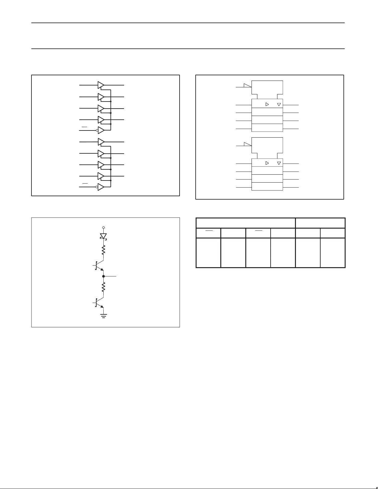
LOGIC SYMBOL
1A0
2
1A1
4
1A2
6
1A3
8
1OE
1
2A3
11
2A2
13
2A1
15
2A0
17
2OE
19
1Y0
1Y1
1Y2
1Y3
2Y3
2Y2
2Y1
2Y0
SA00149
18
16
14
12
9
7
5
3
LOGIC SYMBOL (IEEE/IEC)
1
2
4
6
8
19
11 9
13 7
15 5
17
EN
EN
74ABT2244
18
16
14
12
3
SA00150
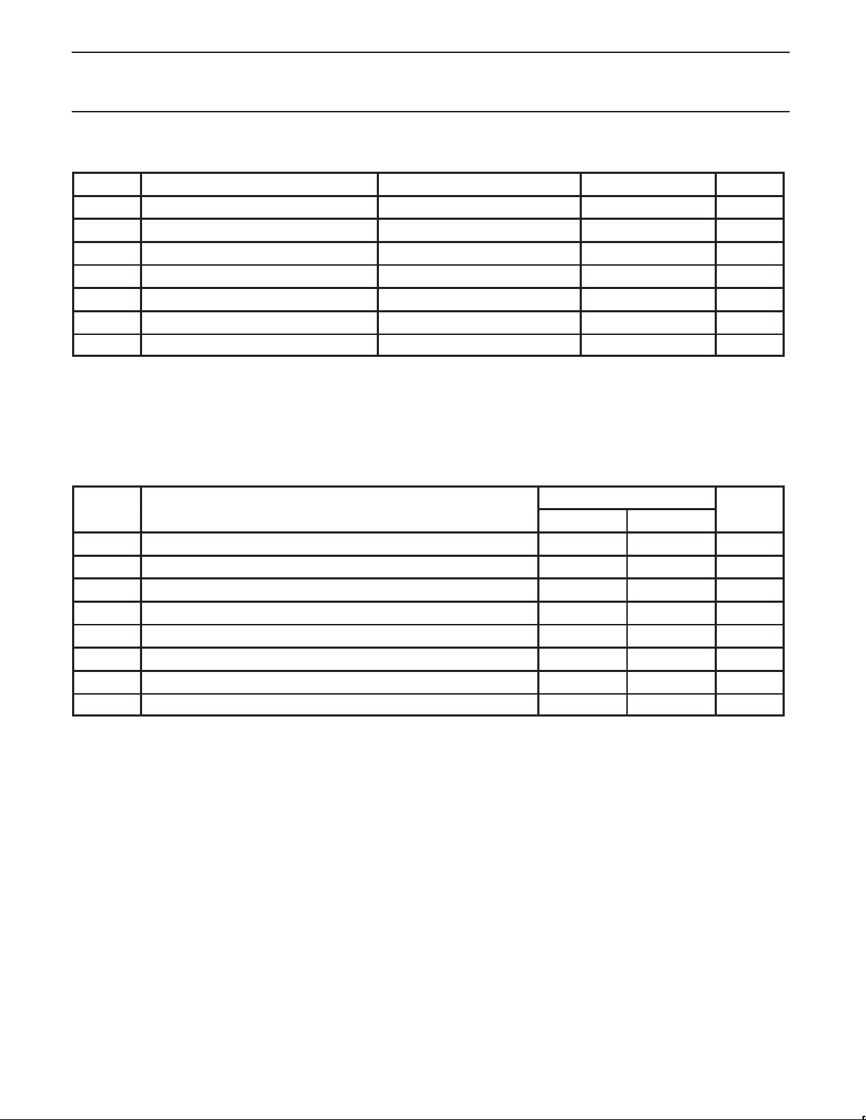
SCHEMATIC OF EACH OUTPUT
V
CC
SA00237
OUTPUT
FUNCTION TABLE
INPUTS OUTPUTS
1OE 1An 2OE 2An 1Yn 2Yn
L L L L L L
L H L H H H
H X H X Z Z
H = High voltage level
L = Low voltage level
X = Don’t care
Z = High impedance “off” state
1998 Jan 16
3
Philips Semiconductors Product specification
SYMBOL
PARAMETER
UNIT
Octal buffer/line driver with 30Ω series
termination resistors (3-State)
ABSOLUTE MAXIMUM RATINGS
SYMBOL
V
V
I
CC
I
IK
V
I
OK
OUT
OUT
T
stg
DC supply voltage –0.5 to +7.0 V
DC input diode current VI < 0 –18 mA
DC input voltage
I
DC output diode current VO < 0 –50 mA
DC output voltage
DC output current output in Low state 128 mA
Storage temperature range –65 to 150 °C
NOTES:
1. Stresses beyond those listed may cause permanent damage to the device. These are stress ratings only and functional operation of the
device at these or any other conditions beyond those indicated under “recommended operating conditions” is not implied. Exposure to
absolute-maximum-rated conditions for extended periods may affect device reliability .
2. The performance capability of a high-performance integrated circuit in conjunction with its thermal environment can create ju nction
temperatures which are detrimental to reliability. The maximum junction temperature of this integrated circuit should not exceed 150°C.
3. The input and output voltage ratings may be exceeded if the input and output current ratings are observed.
PARAMETER CONDITIONS RATING UNIT
3
3
RECOMMENDED OPERATING CONDITIONS
V
CC
V
V
V
I
OH
I
OL
∆t/∆v Input transition rise or fall rate 0 5 ns/V
T
amb
DC supply voltage 4.5 5.5 V
Input voltage 0 V
I
High-level input voltage 2.0 V
IH
Low-level Input voltage 0.8 V
IL
High-level output current –32 mA
Low-level output current 12 mA
Operating free-air temperature range –40 +85 °C
1, 2
–1.2 to +7.0 V
output in Off or High state –0.5 to +5.5 V
LIMITS
Min Max
74ABT2244
CC
V
1998 Jan 16
4
 Loading...