

Philips 74ABT16952 Technical data

查询74ABT16952DGG供应商
INTEGRATED CIRCUITS
74ABT16952
74ABTH16952
16-bit registered transceiver (3-State)
Product specification
Supersedes data of 1995 Sep 28
IC23 Data Handbook
1998 Feb 25
Philips Semiconductors Product specification
Quiescent su ly current
16-bit registered transceiver (3-State)
FEA TURES
•Two 8-bit registered transceivers
•Live insertion/extraction permitted
•Power-up 3-State
•74ABTH16952 incorporates bus-hold data inputs which eliminate
the need for external pull-up resistors to hold unused inputs
•Power-up reset
•Multiple V
•Independent registers for A and B buses
•Output capability: +64mA/–32mA
•Latch-up protection exceeds 500mA per Jedec Std 17
•ESD protection exceeds 2000V per MIL STD 883 Method 3015
and 200V per Machine Model
•Bus-hold data inputs eliminate the need for external pull-up
resistors to hold unused inputs
QUICK REFERENCE DATA
SYMBOL PARAMETER
and GND pins minimize switching noise
CC
t
PLH
t
PHL
C
C
I
CCZ
I
CCL
IN
I/O
Propagation delay
nCPBA to nAx or
nCPAB to nBx
Input capacitance VI = 0V or V
I/O capacitance VO = 0V or VCC; 3-State 7 pF
pp
CL = 50pF; VCC = 5V
Outputs disabled; VCC = 5.5V 500 µA
Outputs LOW; VCC = 5.5V 8 mA
74ABT16952
74ABTH16952
DESCRIPTION
The 74ABT16952 high-performance BiCMOS device combines low
static and dynamic power dissipation with high speed and high
output drive.
The 74ABT16952 is a dual octal registered transceiver. Two 8-bit
registers store data flowing in both directions between two
bidirectional buses. Data applied to the inputs is entered and stored
on the rising edge of the Clock (nCPXX) provided that the Clock
Enable (nCEXX
output buffers, but is only accessible when the Output Enable
(nOEXX) is Low. Data flow from A inputs to B outputs is the same as
for B inputs to A outputs.
Two options are available, 74ABT16952 which does not have the
bus-hold feature and 74ABTH16952 which incorporates the
bus-hold feature.
CONDITIONS
T
= 25°C; GND = 0V
amb
CC
) is Low. The data is then present at the 3-State
TYPICAL UNIT
2.8
2.3
4 pF
ns
ORDERING INFORMATION
PACKAGES TEMPERATURE RANGE OUTSIDE NORTH AMERICA NORTH AMERICA DWG NUMBER
56-Pin Plastic SSOP Type III –40°C to +85°C 74ABT16952 DL BT16952 DL SOT371-1
56-Pin Plastic TSSOP Type II –40°C to +85°C 74ABT16952 DGG BT16952 DGG SOT364-1
56-Pin Plastic SSOP Type III –40°C to +85°C 74ABTH16952 DL BH16952 DL SOT371-1
56-Pin Plastic TSSOP Type II –40°C to +85°C 74ABTH16952 DGG BH16952 DGG SOT364-1
PIN DESCRIPTION
PIN NUMBER SYMBOL NAME AND FUNCTION
2, 55
18, 22
3, 54,
26, 31
52, 51, 49, 48, 47, 45, 44, 43
42, 41, 40, 38, 37, 36, 34, 33
1, 56
8, 29
4, 11, 18, 25, 32, 39, 45, 53
4, 17, 30, 43 GND Ground (0V)
7, 22, 35, 50 V
1CPAB / 1CPBA
2CPAB / 2CPBA
1CEAB / 1CEBA
2CEAB / 2CEBA
1A0 – 1A7
2A0 – 2A7
1B0 – 1B7
2B0 – 2B7
1OEAB / 1OEBA
2OEAB / 2OEBA
CC
Clock input A to B / Clock input B to A
Clock enable input A to B / Clock enable input B to A
Data inputs/outputs (A side)
Data inputs/outputs (B side)
Output enable inputs
Positive supply voltage
1998 Feb 25 853-1814 19018
2

Philips Semiconductors Product specification
16-bit registered transceiver (3-State)
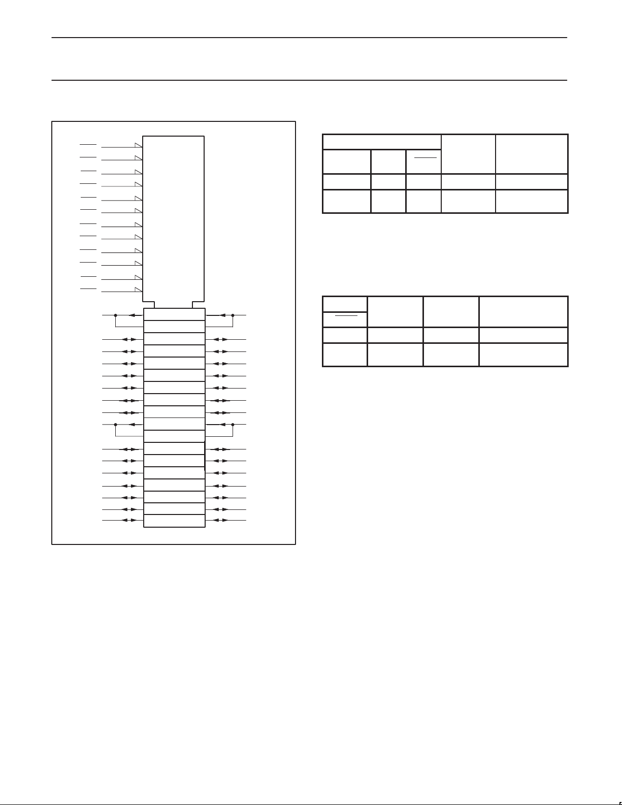
PIN CONFIGURATION
1OEAB
1CPAB
1CEAB
GND
1A0
1A1
V
CC
1A2
1A3
1A4
GND
1A5
1A6
1A7
2A0
2A1
2A2
GND
2A3
2A4
2A5
V
CC
2A6
2A7
GND
2CEAB
2CPAB
2OEAB
1
2
3
4
5
6
7
8
9
10
11
12
13
14
15
16
17
18
19
20
21
22
23
24
25
26
27
28
SH00070
56
1OEBA
55
1CPBA
1CEBA
54
GND
53
1B0
52
1B1
51
50
V
CC
49
1B2
1B3
48
1B4
47
GND
46
1B5
45
1B6
44
1B7
43
2B0
42
41
2B1
2B2
40
GND
39
2B3
38
37
2B4
36
2B5
35
V
CC
34
2B6
33
2B7
32
GND
31
2CEBA
30
2CPBA
29
2OEBA
LOGIC SYMBOL
568910121314
1A0 1A1 1A2 1A3 1A4 1A5 1A6 1A7
2
1CPAB
3
1CEAB
55
1CPBA
54
1CEBA
1B0 1B1 1B2 1B3 1B4 1B5 1B6 1B7
52 51 49 48 47 45 44 43
15 16 17 19 20 21 23 24
2A0 2A1 2A2 2A3 2A4 2A5 2A6 2A7
27
2CPAB
26
2CEAB
30
2CPBA
31
2CEBA
2B0 2B1 2B2 2B3 2B4 2B5 2B6 2B7
42 41 40 38 37 36 34 33
74ABT16952
74ABTH16952
561OEBA
11OEAB
292OEBA
282OEAB
SH00071
1998 Feb 25
3
Philips Semiconductors Product specification
16-bit registered transceiver (3-State)
LOGIC SYMBOL (IEEE/IEC)
1OEBA
1CEBA
1LPBA
1OEAB
1LEAB
1CPAB
2OEBA
2CEBA
2CPBA
2OEAB
2LEAB
2CPAB
1A0
1A1
1A2
1A3
1A4
1A5
1A6
1A7
2A0
2A1
2A2
2A3
2A4
2A5
2A6
2A7
56
54
55
1
3
2
29
31
30
28
26
27
5
6
8
9
10
12
13
14
15
16
17
19
20
21
23
24
1EN3
G1
1C5
EN4
G2
2C6
EN9
G7
7C11
EN10
G8
8C12
∇3
6D 4 ∇
∇911D
12D
5D
10 ∇
52
1B0
51
1B1
49
1B2
48
1B3
47
1B4
45
1B5
44
1B6
43
1B7
42
2B0
41
2B1
40
2B2
38
2B3
37
2B4
36
2B5
34
2B6
33
2B7
74ABT16952
74ABTH16952
FUNCTION TABLE for Register nAx or nBx
INPUTS INTERNAL OPERATING
nAx or
nBx
X X H NC Hold data
L
H
H =High voltage level
L =Low voltage level
↑ =Low-to-High transition
X = Don’t care
XX= AB or BA
NC=No change
FUNCTION TABLE for Output Enable
INPUTS INTERNAL nAx or nBx OPERATING
nOEXX Q OUTPUTS MODE
H X Z Disable outputs
L
L
H =High voltage level
L =Low voltage level
X = Don’t care
XX= AB or BA
Z =High impedance ”off” state
nCPXX nCEXX Q MODE
↑
↑
L
L
L
H
L
H
L
H
Load data
Enable outputs
1998 Feb 25
SH00086
4
 Loading...