

Page 1

Service Manual
43” LCD TV
chassis PL17.03
Contents
43PFL4902/F7 PHILIPS (Serial No.: ME1, ME2)
43PFL5602/F7 PHILIPS (Serial No.: ME1)
43PFL5922/F7 PHILIPS (Serial No.: ME1)
43PFL4902/F8 PHILIPS (Serial No.: FM1)
43PFL5602/F8 PHILIPS (Serial No.: FM1)
This service manual contains information of different types of models.
Make sure to refer to the section describing your model.
© 2017 Funai Electric Co., Ltd.
All rights reserved. No part of this manual may be reproduced, copied, transmitted, disseminated, transcribed,
downloaded or stored in any storage medium, in any form or for any purpose without the express prior written
consent of Funai. Furthermore, any unauthorized commercial distribution of this manual or any revision hereto
is strictly prohibited.
Information in this document is subject to change without notice. Funai reserves the right to change the content
herein without the obligation to notify any person or organization of such changes.
with the design is a registered trademark of Funai Electric Co., Ltd and may not be used in any way
without the express written consent of Funai. All other trademarks used herein remain the exclusive property of
their respective owners. Nothing contained in this manual should be construed as granting, by implication or
otherwise, any license or right to use any of the trademarks displayed herein. Misuse of any trademarks or any
other content in this manual is strictly prohibited. Funai shall aggressively enforce its intellectual property rights
to the fullest extent of the law.
170525
Page 2

IMPORTANT SAFETY NOTICE
The LCD panel is manufactured to provide many years of useful life.
Occasionally a few non active pixels may appear as a tiny spec of color.
This is not to be considered a defect in the LCD screen.
Proper service and repair is important to the safe, reliable operation of all
P&F Equipment. The service procedures recommended by P&F and
described in this service manual are effective methods of performing
service operations. Some of these service special tools should be used
when and as recommended.
It is important to note that this service manual contains various CAUTIONS
and NOTICES which should be carefully read in order to minimize the risk
of personal injury to service personnel. The possibility exists that improper
service methods may damage the equipment. It also is important to
understand that these CAUTIONS and NOTICES ARE NOT EXHAUSTIVE.
P&F could not possibly know, evaluate and advice the service trade of all
conceivable ways in which service might be done or of the possible
hazardous consequences of each way. Consequently, P&F has not
undertaken any such broad evaluation. Accordingly, a servicer who uses a
service procedure or tool which is not recommended by P&F must first use
all precautions thoroughly so that neither his safety nor the safe operation
of the equipment will be jeopardized by the service method selected.
Page 3

TABLE OF CONTENTS
Specifications . . . . . . . . . . . . . . . . . . . . . . . . . . . . . . . . . . . . . . . . . . . . . . . . . . . . . . . . . . . . . . . . . . . . . . . . . . . 1-1
Important Safety Precautions . . . . . . . . . . . . . . . . . . . . . . . . . . . . . . . . . . . . . . . . . . . . . . . . . . . . . . . . . . . . . . . 2-1
Standard Notes for Servicing . . . . . . . . . . . . . . . . . . . . . . . . . . . . . . . . . . . . . . . . . . . . . . . . . . . . . . . . . . . . . . . 3-1
Cabinet Disassembly Instructions . . . . . . . . . . . . . . . . . . . . . . . . . . . . . . . . . . . . . . . . . . . . . . . . . . . . . . . . . . . 4-1
Electrical Adjustment Instructions . . . . . . . . . . . . . . . . . . . . . . . . . . . . . . . . . . . . . . . . . . . . . . . . . . . . . . . . . . . 5-1
How to Initialize the LCD TV . . . . . . . . . . . . . . . . . . . . . . . . . . . . . . . . . . . . . . . . . . . . . . . . . . . . . . . . . . . . . . . . 6-1
Firmware Renewal Mode [55PFL5602/F7] . . . . . . . . . . . . . . . . . . . . . . . . . . . . . . . . . . . . . . . . . . . . . . . . . . . . . 7-1
Firmware Renewal Mode [55PFL5922/F7] . . . . . . . . . . . . . . . . . . . . . . . . . . . . . . . . . . . . . . . . . . . . . . . . . . . . . 7-3
Troubleshooting . . . . . . . . . . . . . . . . . . . . . . . . . . . . . . . . . . . . . . . . . . . . . . . . . . . . . . . . . . . . . . . . . . . . . . . . . 8-1
Block Diagrams . . . . . . . . . . . . . . . . . . . . . . . . . . . . . . . . . . . . . . . . . . . . . . . . . . . . . . . . . . . . . . . . . . . . . . . . . 9-1
Schematic Diagrams / CBA and Test Points. . . . . . . . . . . . . . . . . . . . . . . . . . . . . . . . . . . . . . . . . . . . . . . . . . . 10-1
Wiring Diagram . . . . . . . . . . . . . . . . . . . . . . . . . . . . . . . . . . . . . . . . . . . . . . . . . . . . . . . . . . . . . . . . . . . . . . . . 11-1
Exploded Views. . . . . . . . . . . . . . . . . . . . . . . . . . . . . . . . . . . . . . . . . . . . . . . . . . . . . . . . . . . . . . . . . . . . . . . . . 12-1
Parts List . . . . . . . . . . . . . . . . . . . . . . . . . . . . . . . . . . . . . . . . . . . . . . . . . . . . . . . . . . . . . . . . . . . . . . . . . . . . . . 13-1
Revision History . . . . . . . . . . . . . . . . . . . . . . . . . . . . . . . . . . . . . . . . . . . . . . . . . . . . . . . . . . . . . . . . . . . . . . . . 14-1
Page 4
SPECIFICATIONS
< TUNER / NTSC >
Description Condition Unit Nominal Limit
1. AFT Pull-In Range --- MHz ±2.3 ±2.1
18
18
18
2. Synchronizing Sens.
TV.ch.4
CA.ch.31
CA.ch.87
dBV
dBV
dBV
< TUNER / ATSC >
Description Condition Unit Nominal Limit
1. Received Freq. Range (-28dBm) --- kHz --- ±100
2. ATSC Dynamic Range (min / max)
ch.4
ch.10
ch.41
dBm
dBm
dBm
---
---
---
< LCD PANEL >
Description Condition Unit Nominal Limit
1. Native Pixel Resolution
2. Brightness (w / filter) ---
3. Viewing Angle
Horizontal
Vertical
Horizontal
Vertical
pixels
pixels
cd/m
°
°
3840
2160
2
400 ---
-88 to 88
-88 to 88
20
20
23
-76/0
-76/0
-76/+4
---
---
---
---
< VIDEO >
Description Condition Unit Nominal Limit
1. Over Scan
2. Color Temperature
3. Resolution (composite video)
Horizontal
Vertical
--x
y
<Measurement condition>
Input signal: HDMI1 Raster (40/80IRE) 1080i@60
Measurement point: Screen center
Measuring instrument:
Aging time: 60min. (Retail MODE / 100IRE Raster HDMI
MODE setting of TV: Shipment setting / Retail MODE
Ambient temperature: 25°C ±5°C
Horizontal
Vertical
%
%
°K 12000
Made of KONICA MINOLTA Luminance meter CA310
1080i@60)
line
line
5
5
0.272
0.278
400
350
5±5
5±5
--±3%
±3%
---
---
< AUDIO >
All items are measured across 8 load at speaker output terminal with L.P.F.
Description Condition Unit Nominal Limit
1.
Audio MAX Output (ATSC 0dBfs)
2. Audio Distortion (NTSC) 500mW: Lch/Rch % 0.5/0.5 2.0/2.0
Lch/Rch W 10.0/10.0 9.0/9.0
1-1 PL17.06-A_SP
Page 5
IMPORTANT SAFETY PRECAUTIONS
Prior to shipment from the factory, our products are strictly inspected for recognized product safety and electrical
codes of the countries in which they are to be sold. However, in order to maintain such compliance, it is equally
important to implement the following precautions when a set is being serviced.
Safety Precautions for LCD TV
Circuit
1. Before returning an instrument to the
customer, always make a safety check of the
entire instrument, including, but not limited to, the
following items:
a. Be sure that no built-in protective devices are
defective and have been defeated during
servicing. (1) Protective shields are provided
on this chassis to protect both the technician
and the customer. Correctly replace all missing
protective shields, including any removed for
servicing convenience. (2) When reinstalling
the chassis and/or other assembly in the
cabinet, be sure to put back in place all
protective devices, including but not limited to,
nonmetallic control knobs, insulating
fishpapers, adjustment and compartment
covers/shields, and isolation resistor/capacitor
networks. Do not operate this instrument or
permit it to be operated without all
protective devices correctly installed and
functioning. Servicers who defeat safety
features or fail to perform safety checks
may be liable for any resulting damage.
b. Be sure that there are no cabinet openings
through which an adult or child might be able to
insert their fingers and contact a hazardous
voltage. Such openings include, but are not
limited to, (1) spacing between the Liquid
Crystal Panel and the cabinet mask, (2)
excessively wide cabinet ventilation slots, and
(3) an improperly fitted and/or incorrectly
secured cabinet back cover.
c. Antenna Cold Check - With the instrument AC
plug removed from any AC source, connect an
electrical jumper across the two AC plug
prongs. Place the instrument AC switch in the
on position. Connect one lead of an ohmmeter
to the AC plug prongs tied together and touch
the other ohmmeter lead in turn to each tuner
antenna input exposed terminal screw and, if
applicable, to the coaxial connector. If the
measured resistance is less than 1.0 megohm
or greater than 5.2 megohm, an abnormality
exists that must be corrected before the
instrument is returned to the customer. Repeat
this test with the instrument AC switch in the off
position.
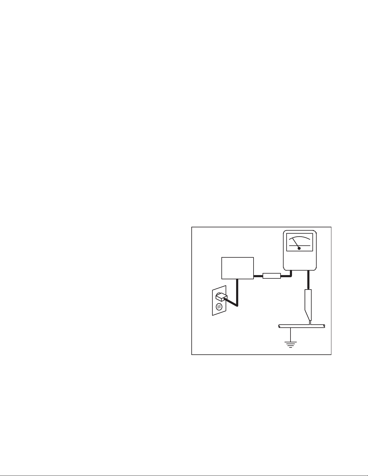
d. Leakage Current Hot Check - With the
instrument completely reassembled, plug the
AC line cord directly into a 120 V AC outlet. (Do
not use an isolation transformer during this
test.) Use a leakage current tester or a
metering system that complies with American
National Standards Institute (ANSI) C101.1
Leakage Current for Appliances and
Underwriters Laboratories (UL) 1410, (50.7).
With the instrument AC switch first in the on
position and then in the off position, measure
from a known earth ground (metal water pipe,
conduit, etc.) to all exposed metal parts of the
instrument (antennas, handle brackets, metal
cabinet, screw heads, metallic overlays, control
shafts, etc.), especially any exposed metal
parts that offer an electrical return path to the
chassis. Any current measured must not
exceed 0.5 milli-ampere. Reverse the
instrument power cord plug in the outlet and
repeat the test.
READING SHOULD
NOT BE ABOVE 0.5 mA
LEAKAGE
DEVICE
BEING
TESTED
TEST ALL EXPOSED
METAL SURFACES
ALSO TEST WITH
PLUG REVERSED
USING AC
ADAPTER PLUG
AS REQUIRED
ANY MEASUREMENTS NOT WITHIN THE
LIMITS SPECIFIED HEREIN INDICATE A
POTENTIAL SHOCK HAZARD THAT MUST
BE ELIMINATED BEFORE RETURNING THE
INSTRUMENT TO THE CUSTOMER OR
BEFORE CONNECTING THE ANTENNA OR
ACCESSORIES.
2. Read and comply with all caution and safety-
related notes on or inside the receiver cabinet, on
the receiver chassis, or on the Liquid Crystal
Panel.
CURRENT
TESTER
+
EARTH
GROUND
_
2-1 LTVN_ISP
Page 6

3. Design Alteration Warning - Do not alter or add
to the mechanical or electrical design of this TV
receiver. Design alterations and additions,
including, but not limited to circuit modifications
and the addition of items such as auxiliary audio
and/or video output connections, might alter the
safety characteristics of this receiver and create a
hazard to the user. Any design alterations or
additions will void the manufacturer's warranty and
may make you, the servicer, responsible for
personal injury or property damage resulting
therefrom.
4. Hot Chassis Warning a. Some TV receiver chassis are electrically
connected directly to one conductor of the AC
power cord and maybe safety-serviced without
an isolation transformer only if the AC power
plug is inserted so that the chassis is
connected to the ground side of the AC power
source. To confirm that the AC power plug is
inserted correctly, with an AC voltmeter,
measure between the chassis and a known
earth ground. If a voltage reading in excess of
1.0 V is obtained, remove and reinsert the AC
power plug in the opposite polarity and again
measure the voltage potential between the
chassis and a known earth ground.
b. Some TV receiver chassis normally have 85V
AC(RMS) between chassis and earth ground
regardless of the AC plug polarity. This chassis
can be safety-serviced only with an isolation
transformer inserted in the power line between
the receiver and the AC power source, for both
personnel and test equipment protection.
c. Some TV receiver chassis have a secondary
ground system in addition to the main chassis
ground. This secondary ground system is not
isolated from the AC power line. The two
ground systems are electrically separated by
insulation material that must not be defeated or
altered.
5. Observe original lead dress. Take extra care to
assure correct lead dress in the following areas: a.
near sharp edges, b. near thermally hot parts-be
sure that leads and components do not touch
thermally hot parts, c. the AC supply, d. high
voltage, and, e. antenna wiring. Always inspect in
all areas for pinched, out of place, or frayed wiring.
Check AC power cord for damage.
6. Components, parts, and/or wiring that appear to
have overheated or are otherwise damaged
should be replaced with components, parts, or
wiring that meet original specifications.
Additionally, determine the cause of overheating
and/or damage and, if necessary, take corrective
action to remove any potential safety hazard.
7. Product Safety Notice - Some electrical and
mechanical parts have special safety-related
characteristics which are often not evident from
visual inspection, nor can the protection they give
necessarily be obtained by replacing them with
components rated for higher voltage, wattage, etc.
Parts that have special safety characteristics are
identified by a # on schematics and in parts lists.
Use of a substitute replacement that does not
have the same safety characteristics as the
recommended replacement part might create
shock, fire, and/or other hazards. The product's
safety is under review continuously and new
instructions are issued whenever appropriate.
Prior to shipment from the factory, our products
are strictly inspected to confirm they comply with
the recognized product safety and electrical codes
of the countries in which they are to be sold.
However, in order to maintain such compliance, it
is equally important to implement the following
precautions when a set is being serviced.
2-2 LTVN_ISP
Page 7

Precautions during Servicing
A. Parts identified by the # symbol are critical for
safety.
Replace only with part number specified.
B. In addition to safety, other parts and assemblies
are specified for conformance with regulations
applying to spurious radiation. These must also be
replaced only with specified replacements.
Examples: RF converters, RF cables, noise
blocking capacitors, and noise blocking filters, etc.
C. Use specified internal wiring. Note especially:
1) Wires covered with PVC tubing
2) Double insulated wires
3) High voltage leads
D. Use specified insulating materials for hazardous
live parts. Note especially:
1) Insulation Tape
2) PVC tubing
3) Spacers
4) Insulators for transistors.
E. When replacing AC primary side components
(transformers, power cord, etc.), wrap ends of
wires securely about the terminals before
soldering.
F. Observe that the wires do not contact heat
producing parts (heat sinks, oxide metal film
resistors, fusible resistors, etc.)
G. Check that replaced wires do not contact sharp
edged or pointed parts.
H. When a power cord has been replaced, check that
11~13 lb (5~6 kg) of force in any direction will not
loosen it.
I. Also check areas surrounding repaired locations.
J. Use care that foreign objects (screws, solder
droplets, etc.) do not remain inside the set.
K. When connecting or disconnecting the internal
connectors, first, disconnect the AC plug from the
AC supply outlet.
L. When installing parts or assembling the cabinet
parts, be sure to use the proper screws and
tighten certainly.
2-3 LTVN_ISP
Page 8
Safety Check after Servicing
Examine the area surrounding the repaired location for damage or deterioration. Observe that screws, parts and
wires have been returned to original positions. Afterwards, perform the following tests and confirm the specified
values in order to verify compliance with safety standards.
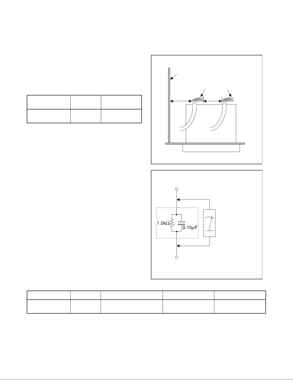
1. Clearance Distance
When replacing primary circuit components, confirm
specified clearance distance (d) and (d') between
soldered terminals, and between terminals and
surrounding metallic parts. (See Fig. 1)
Table 1: Ratings for selected area
Chassis or Secondary Conductor
Primary Circuit
AC Line Voltage Region
110 to 130 V
Note: This table is unofficial and for reference only. Be
sure to confirm the precise values.
U.S.A. or
Canada
Clearance
Distance (d), (d’)
3.2 mm
(0.126 inches)
2. Leakage Current Test
Confirm the specified (or lower) leakage current
between B (earth ground, power cord plug prongs) and
externally exposed accessible parts (RF terminals,
antenna terminals, video and audio input and output
terminals, microphone jacks, earphone jacks, etc.) is
lower than or equal to the specified value in the table
below.
Measuring Method: (Power ON)
Insert load Z between B (earth ground, power cord plug
prongs) and exposed accessible parts. Use an AC
voltmeter to measure across both terminals of load Z.
See Fig. 2 and following table.
d' d
Fig. 1
Exposed Accessible Part
Z
AC Voltmeter
(High Impedance)
Earth Ground
B
Power Cord Plug Prongs
Fig. 2
Table 2: Leakage current ratings for selected areas
AC Line Voltage Region Load Z Leakage Current (i) Earth Ground (B) to:
110 to 130 V
Note: This table is unofficial and for reference only. Be sure to confirm the precise values.
U.S.A. or
Canada
0.15 F CAP. & 1.5 k
RES. Connected in parallel
2-4 LTVN_ISP
i 0.5 mA rms
Exposed accessible
parts
Page 9
STANDARD NOTES FOR SERVICING
To p Vi ew
Out
In
Bottom View
Input
5
10
Pin 1
Pin 1
Circuit Board Indications
1. The output pin of the 3 pin Regulator ICs is
indicated as shown.
2. For other ICs, pin 1 and every fifth pin are
indicated as shown.
3. The 1st pin of every male connector is indicated
as shown.
Pb (Lead) Free Solder
Pb free mark will be found on PCBs which use Pb
free solder. (Refer to figure.) For PCBs with Pb free
mark, be sure to use Pb free solder. For PCBs
without Pb free mark, use standard solder.
Pb free mark
How to Remove / Install Flat Pack-IC
1. Removal
With Hot-Air Flat Pack-IC Desoldering Machine:
1. Prepare the hot-air flat pack-IC desoldering
machine, then apply hot air to the Flat Pack-IC
(about 5 to 6 seconds). (Fig. S-1-1)
Fig. S-1-1
2. Remove the flat pack-IC with tweezers while
applying the hot air.
3. Bottom of the flat pack-IC is fixed with glue to the
CBA; when removing entire flat pack-IC, first apply
soldering iron to center of the flat pack-IC and heat
up. Then remove (glue will be melted). (Fig. S-1-6)
4. Release the flat pack-IC from the CBA using
tweezers. (Fig. S-1-6)
CAUTION:
1. The Flat Pack-IC shape may differ by models. Use
an appropriate hot-air flat pack-IC desoldering
machine, whose shape matches that of the Flat
Pack-IC.
2. Do not supply hot air to the chip parts around the
flat pack-IC for over 6 seconds because damage
to the chip parts may occur. Put masking tape
around the flat pack-IC to protect other parts from
damage. (Fig. S-1-2)
3-1 TVN_SN
Page 10
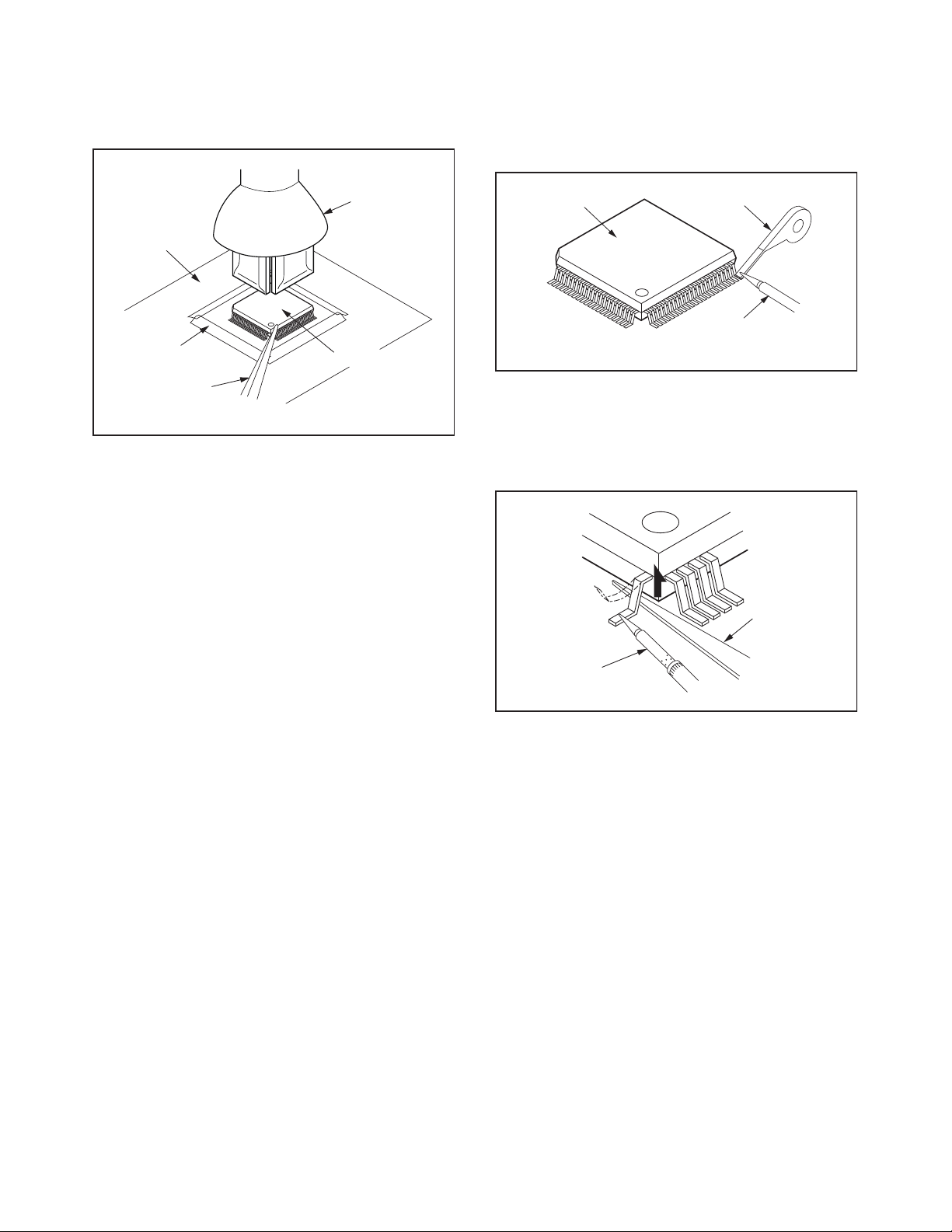
3. The flat pack-IC on the CBA is affixed with glue, so
Hot-air
Flat Pack-IC
Desoldering
Machine
CBA
Flat Pack-IC
Tweezers
Masking
Ta pe
Fig. S-1-2
be careful not to break or damage the foil of each
pin or the solder lands under the IC when
removing it.
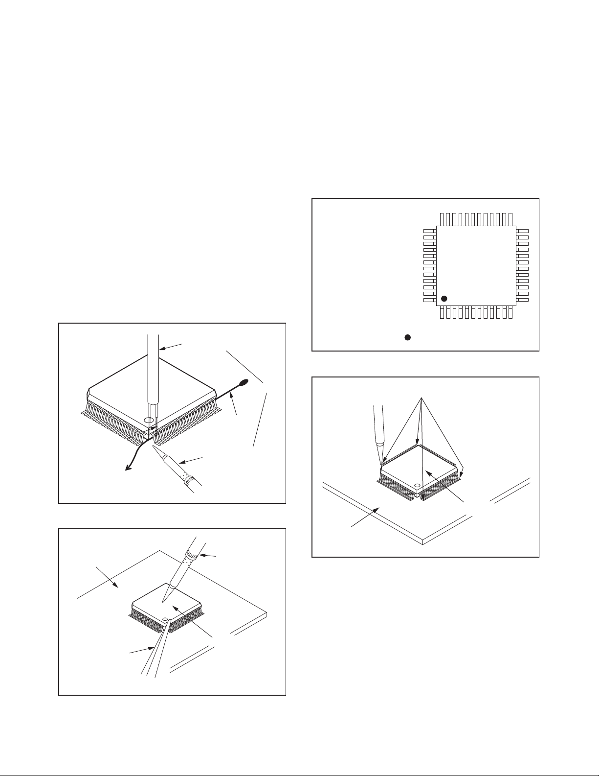
With Soldering Iron:
1. Using desoldering braid, remove the solder from
all pins of the flat pack-IC. When you use solder
flux which is applied to all pins of the flat pack-IC,
you can remove it easily. (Fig. S-1-3)
Flat Pack-IC
Desoldering Braid
Soldering Iron
Fig. S-1-3
2. Lift each lead of the flat pack-IC upward one by
one, using a sharp pin or wire to which solder will
not adhere (iron wire). When heating the pins, use
a fine tip soldering iron or a hot air desoldering
machine. (Fig. S-1-4)
Sharp
Pin
Fine Tip
Soldering Iron
3. Bottom of the flat pack-IC is fixed with glue to the
CBA; when removing entire flat pack-IC, first apply
soldering iron to center of the flat pack-IC and heat
up. Then remove (glue will be melted). (Fig. S-1-6)
4. Release the flat pack-IC from the CBA using
tweezers. (Fig. S-1-6)
Fig. S-1-4
3-2 TVN_SN
Page 11
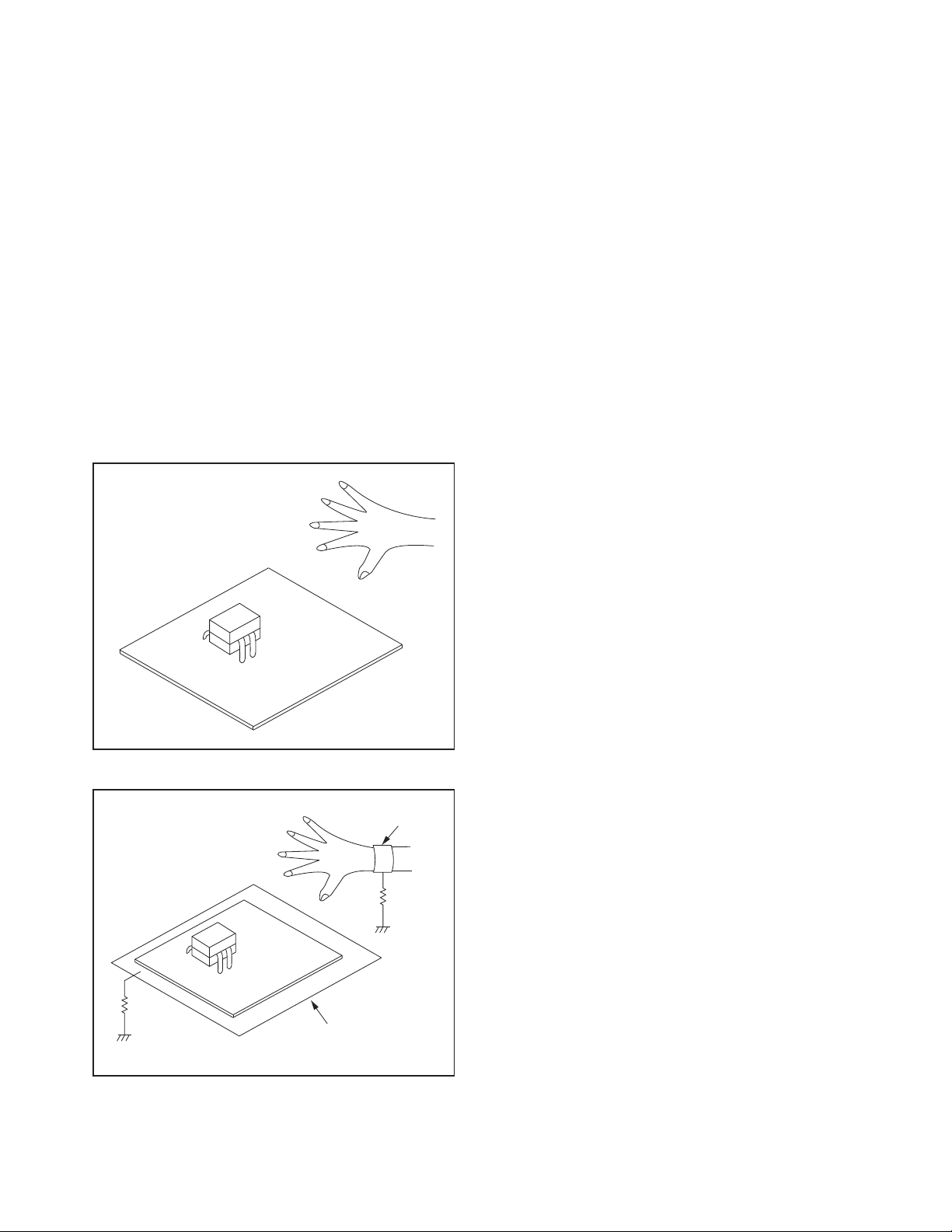
With Iron Wire:
To Solid
Mounting Point
Soldering Iron
Iron Wire
or
Hot Air Blower
Fig. S-1-5
Fine Tip
Soldering Iron
CBA
Flat Pack-IC
Tweezers
Fig. S-1-6
1. Using desoldering braid, remove the solder from
all pins of the flat pack-IC. When you use solder
flux which is applied to all pins of the flat pack-IC,
you can remove it easily. (Fig. S-1-3)
2. Affix the wire to a workbench or solid mounting
point, as shown in Fig. S-1-5.
3. While heating the pins using a fine tip soldering
iron or hot air blower, pull up the wire as the solder
melts so as to lift the IC leads from the CBA
contact pads as shown in Fig. S-1-5.
4. Bottom of the flat pack-IC is fixed with glue to the
CBA; when removing entire flat pack-IC, first apply
soldering iron to center of the flat pack-IC and heat
up. Then remove (glue will be melted). (Fig. S-1-6)
5. Release the flat pack-IC from the CBA using
tweezers. (Fig. S-1-6)
Note: When using a soldering iron, care must be
taken to ensure that the flat pack-IC is not
being held by glue. When the flat pack-IC is
removed from the CBA, handle it gently
because it may be damaged if force is applied.
2. Installation
1. Using desoldering braid, remove the solder from
the foil of each pin of the flat pack-IC on the CBA
so you can install a replacement flat pack-IC more
easily.
2. The “ I ” mark on the flat pack-IC indicates pin 1.
(See Fig. S-1-7.) Be sure this mark matches the
pin 1 on the PCB when positioning for installation.
Then presolder the four corners of the flat pack-IC.
(See Fig. S-1-8.)
3. Solder all pins of the flat pack-IC. Be sure that
none of the pins have solder bridges.
Example :
Pin 1 of the Flat Pack-IC
is indicated by a " " mark.
Fig. S-1-7
Presolder
Flat Pack-IC
CBA
Fig. S-1-8
3-3 TVN_SN
Page 12
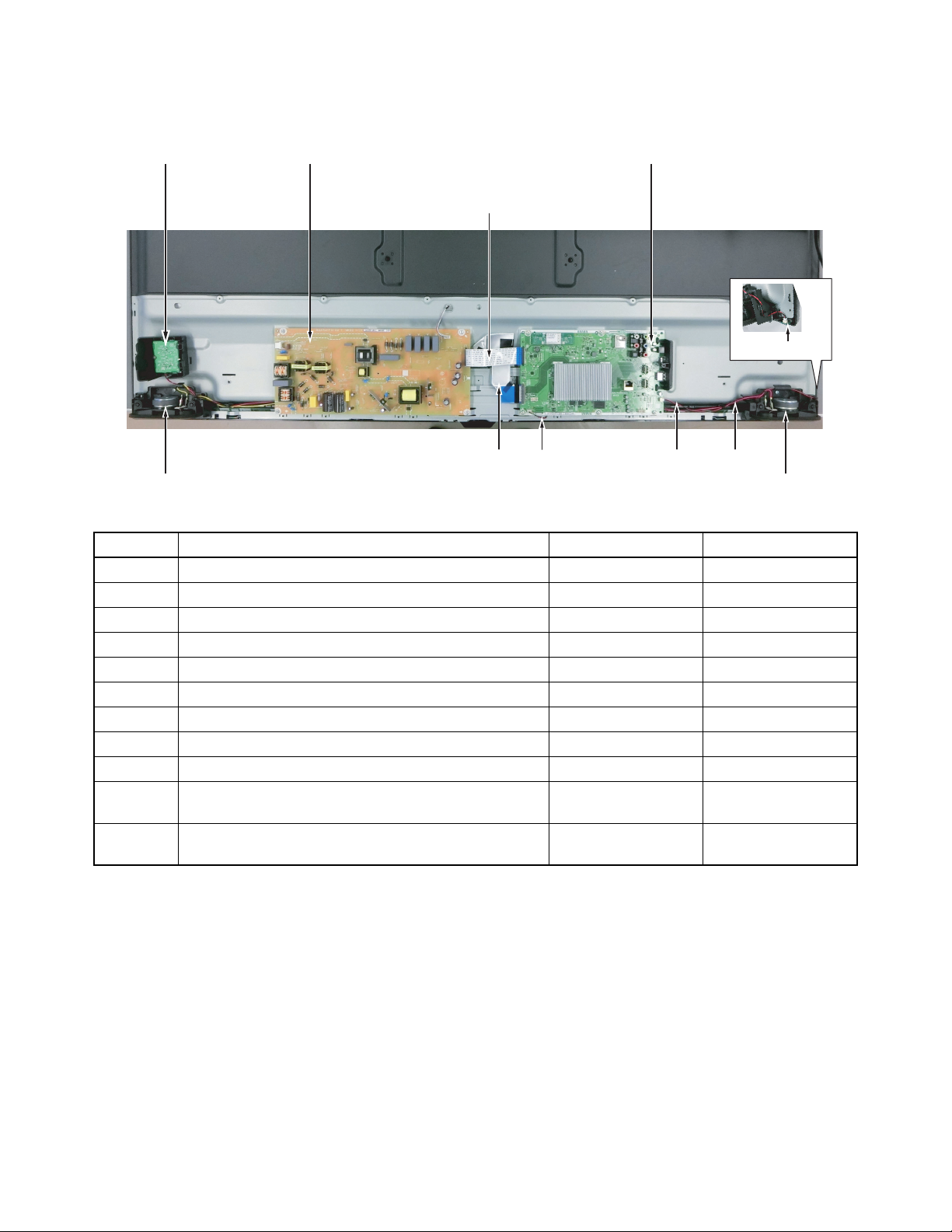
Instructions for Handling Semi-
<Incorrect>
CBA
Grounding Band
Conductive Sheet or
Copper Plate
1MΩ
1MΩ
<Correct>
CBA
conductors
Electrostatic breakdown of the semi-conductors may
occur due to a potential difference caused by
electrostatic charge during unpacking or repair work.
1. Ground for Human Body
Be sure to wear a grounding band (1 M) that is
properly grounded to remove any static electricity that
may be charged on the body.
2. Ground for Workbench
Be sure to place a conductive sheet or copper plate
with proper grounding (1 M) on the workbench or
other surface, where the semi-conductors are to be
placed. Because the static electricity charge on
clothing will not escape through the body grounding
band, be careful to avoid contacting semi-conductors
with your clothing.
3-4 TVN_SN
Page 13
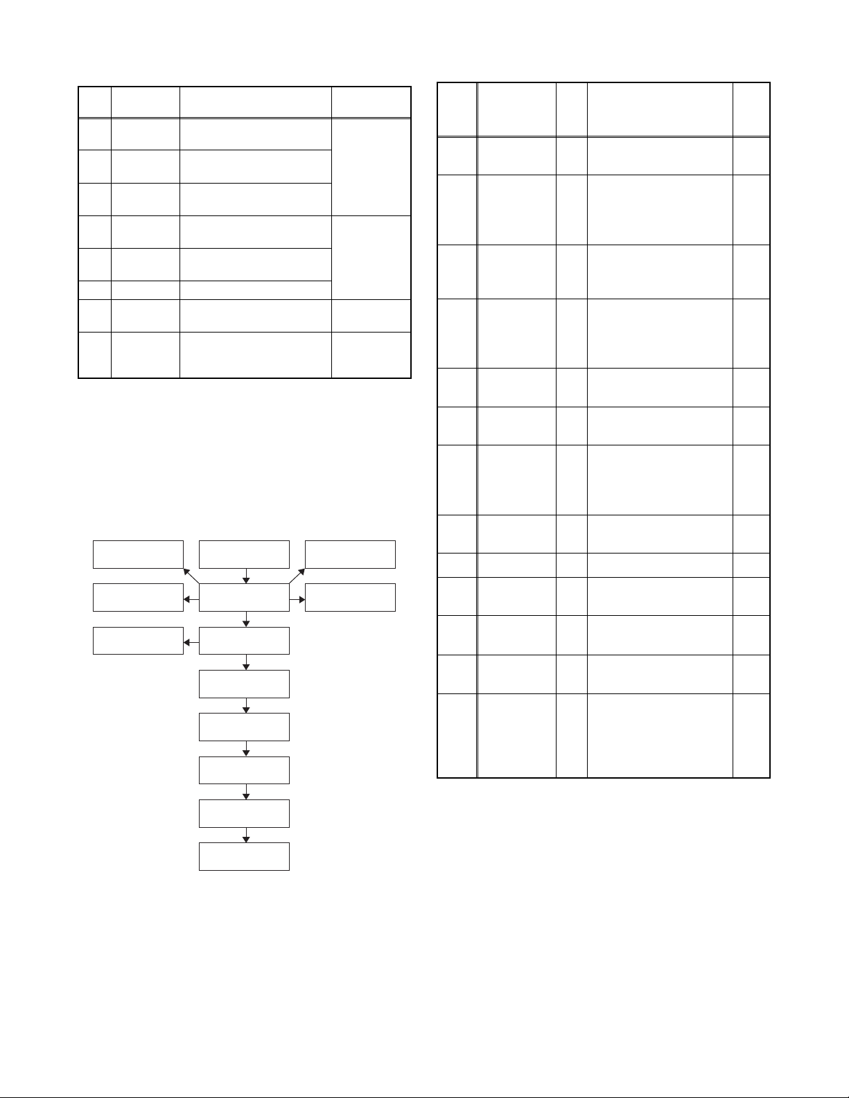
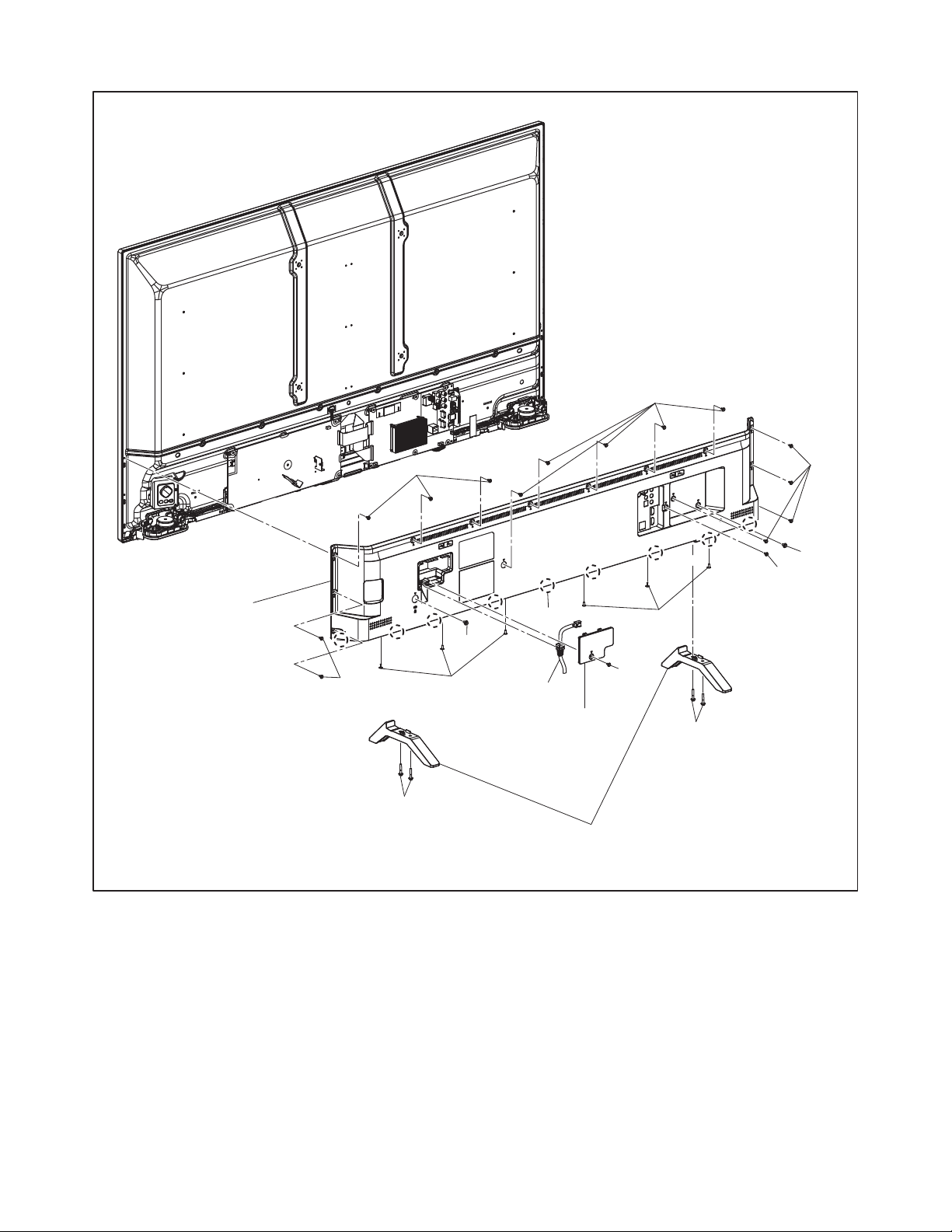
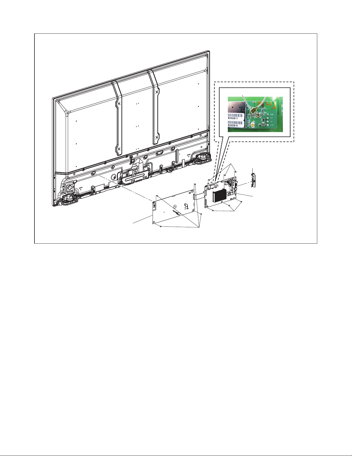
CABINET DISASSEMBLY INSTRUCTIONS
Power Supply CBAFunction CBA Digital Main CBA Unit
CL3601
IR Sensor CBA Unit
CL3901 CL3105
Ref.No. Description Part Number Type
Digital Main CBA Unit AA7R1MMA-001 55PFL5602/F7
Digital Main CBA Unit AA7RZMMA-001 55PFL5922/F7
Function CBA AA7R1MSW-001
IR Sensor CBA Unit AA7R1MJC-001
Power Supply CBA AA7R1MPW-001
CL3103 WIRE ASSEMBLY 3PIN 3PIN/365MM WX1AA7R1T411
CL3105 WIRE ASSEMBLY 2PIN 2PIN/750MM WX1AA7R1T311
CL3601 WIRE ASSEMBLY 27PIN 27PIN/115MM WX1AA7R1T111
CL3801 WIRE ASSEMBLY 4PIN 4PIN/280MM&850MM WX1AA7R1C221
CL3901
SP3801
SP3802
FFC WIRE ASSEMBLY 51PIN(W/SHIELD) 51P/
FFC/SHIELD/251MM
SPEAKER MAGNETIC 8OHM/10W S0411F19 DS08110XQ004
WX1AA7R1T501
CL3103
CL3801
SpeakerSpeaker
4-1 PL17.06-A_DC
Page 14
Screw Torque Specification
2. Disassembly Method
Ref.
No.
L23 GBJS3060
L45 FPH34100
L73 GCHP3100
L83 GCHP3080
L95 2EML00029 SCREW M3X5 LOW HEAD
L128 2EML00041
SSK1 2ESA04123
Part
Number
Part Name
SCREW BIND 3CHROM
+S-TITE M3X6.0
SCREW F-PAN BLACK_NI
+S-TITE M3X8.0
SEMS-SW PAN BLACK_NI
+ M4X10.0
SCREW F-PAN BLACK_NI
+P-TITE M3X10
SCREW F-PAN BLACK_NI
+P-TITE M3X8
SCREW M3X8 WIDTH
LOW HEAD BLACK
STAND SCREW KIT
AA7R1UH (DOUBLE SEMS
SCREW M4X25 +BLK)
Tightening
Torque
6.1±0.9lb·inL28 GCHS3080
5.2±0.9lb·in
6.1±0.9lb·in
(approx.
8.7±0.9lb·in)
*: For reference
1. Disassembly Flowchart
This flowchart indicates the disassembly steps for the
cabinet parts and the CBA in order to gain access to
items to be serviced. When reassembling, follow the
steps in reverse order. Bend, route and dress the
cables as they were.
[7] Function CBA
[1] Stand
Assembly
[8] IR Sensor
CBA Unit
Step/
Loc.
No.
[1]
Part
Stand
Assembly
Fig.
No.
Removal Note
D1 4(S-1) ---
14(S-2), 2(S-3),
D1
[2] Rear Cover
2(S-4), 6(S-5), 9(L-1),
W1
CN601, AC Cord
---
Cover, AC Cord
[3]
Power
Supply
CBA
D2W14(S-6), CN651,
CN1001
---
6(S-7), CN3103,
Digital Main
[4]
CBA UnitD2W1
*
PCB Holder
[5]
B
PCB Holder
[6]
A
CN3105, CN3801,
CN3901, CON1
*4
,
---
Jack Holder
D3 2(S-8) ---
D3 3(S-9) ---
(S-10), Knob Frame,
[7]
Function
CBA
Switch Shield,
D4
Function Knob, Hook,
W1
2
Wire Label
IR Sensor
[8]
CBA UnitD4W1
Sensor Lens, Sensor
Shireld
2
[9] Speaker D4 ---------- ---
[3] Power
Supply CBA
[11] T-CON Holder
[2] Rear Cover
[5] PCB Holder B
[6] PCB Holder A
[9] Speaker
[10] Speaker
Holder L, R
[12] LCD Panel
Assembly
[13] Front Cabinet
[4] Digital Main
CBA Unit
Speaker
[10]
[11]
[12]
Holder L, R
T-CON
Holder
LCD Panel
Assembly
D4 2(S-11) ---
4(S-12), T-CON
D5
Module, FFC Cable
D5 3(S-13) 1
1
Cell Cushion UD, Cell
Cushion LR, Gasket,
D5
Grand Tape U, Grand
Tape S, Decoration
3
[13]
Front
Cabinet
Plate
(1)
(2)
(3)
(4)
(5)
*4: 55PFL5922/F7
Note:
(1) Order of steps in procedure. When reassembling,
follow the steps in reverse order. These numbers
are also used as the Identification (location) No. of
parts in figures.
(2) Parts to be removed or installed.
(3) Fig. No. showing procedure of part location
4-2 PL17.06-A_DC
Page 15

(4) Identification of parts to be removed, unhooked,
unlocked, released, unplugged, unclamped, or
desoldered.
P = Spring, L = Locking Tab, S = Screw,
H = Hex Screw, CN = Connector
e.g. 2(S-2) = two Screws of (S-2),
2(L-2) = two Locking Tabs of (L-2)
(5) Refer to the following “Reference Notes in the
Table.”
Important precautions concerning the
LCD Panel Assembly:
1. When you disassemble/re-assemble the LCD
Panel Assembly.
• Do not pull the FFC Cable and Board Cable
forcefully when you re-assemble.
• Be careful not to scratch the display panel when
assembling.
• Make sure to replace the Decoration Plate to a new
one when replacing the LCD Panel Assembly.
• Make sure the T-CON Module and T-CON Holder
are securely in place when re-assembling.
2. When you disassemble/re-assemble the
Function CBA or the IR Sensor CBA Unit.
• Be careful not to scratch the display panel when
assembling.
• The Function CBA Unit, Function Knob, Switch
Shield and Knob Frame are fixed in place by the
hooks. Make sure these hooks are not damaged.
Make sure the Function CBA Unit, Function Knob
and Knob Frame.
• Make sure the tact switches operate normally after
replacing the Function CBA.
• Make sure the Sensor Shield, Sensor Lens and IR
Sensor CBA Unit are securely in place when reassembling.
3. When you disassemble/re-assemble the Front
Cabinet.
• Be careful not to break the hook. If you pull with too
much force, the hooks may be damaged.
• Make sure to replace the Cell Cushion, Gasket,
Grand Tape and Decoraion Plate to a new one when
replacing the Front Cabinet.
4-3 PL17.06-A_DC
Page 16
(S-1)
(S-1)
(S-2)
(S-2)
(S-3)
(S-3)
(S-4)
(S-5)
(S-5)
(S-4)
(S-2)
(S-2)
AC Cord Cover
AC Cord
[2] Rear Cover
[1] Stand Assembly
(L-1)
Fig. D1
4-4 PL17.06-A_DC
Page 17
[4] Digital Main
CBA Unit
[3] Power Supply CBA
(S-6)
Jack Holder
(S-7)
(S-7)
CON1
55PFL5922/F7
Fig. D2
4-5 PL17.06-A_DC
Page 18
[5] PCB Holder B
[6] PCB Holder A
(S-8)
(S-9)
(S-9)
Fig. D3
4-6 PL17.06-A_DC
Page 19
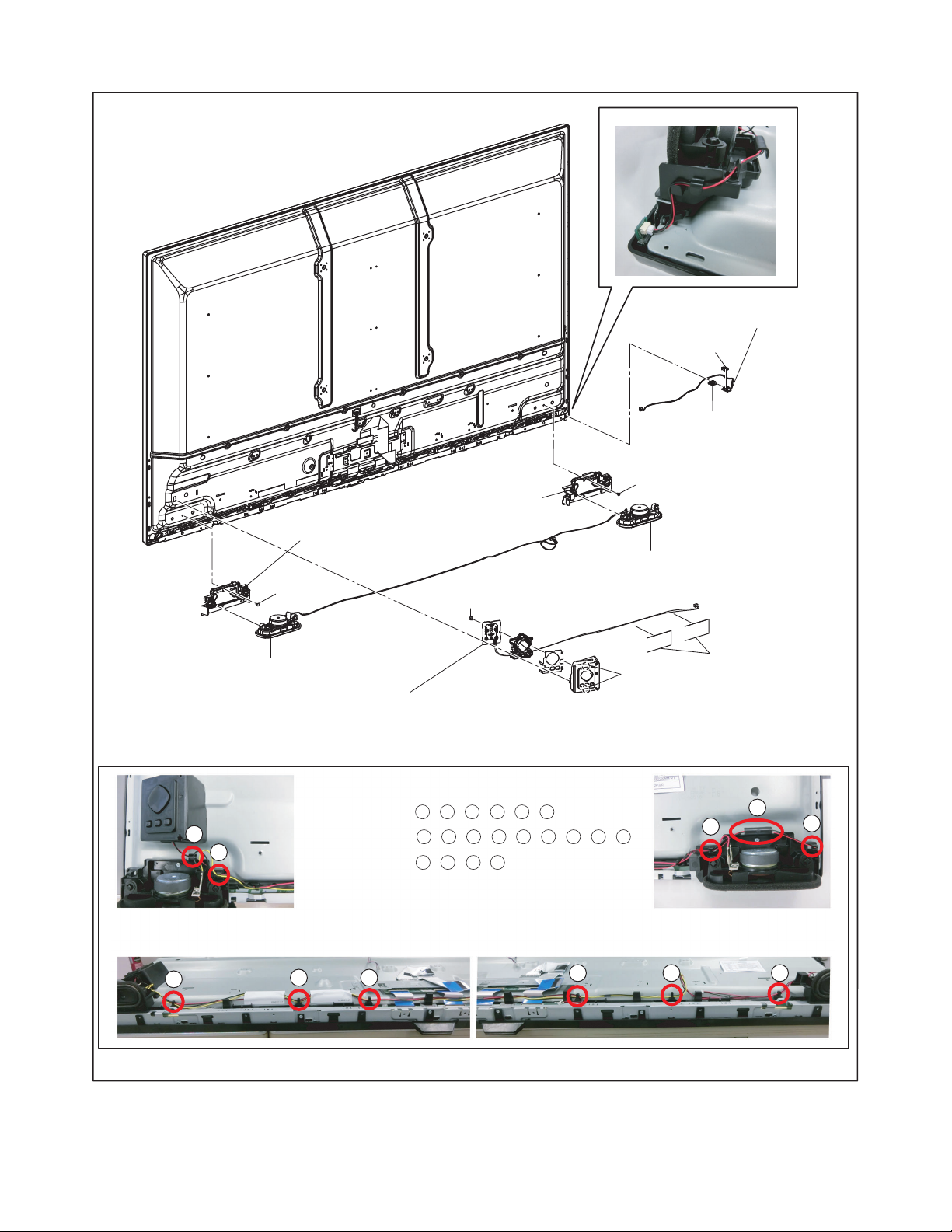
[9] Speaker
(S-10)
(S-11)
(S-11)
Sensor Shield*
2
Wire Label
Sensor Lens*
2
Function Knob*
2
Knob Frame*
2
Switch Shield*
2
[7] Function CBA
*
2
[8] IR Sensor CBA Unit
*
2
Hook*
2
Wire of Function 1 - 2 - 3 - 4 - 5 - 6
[9] Speaker
[10] Speaker Holder L
[10] Speaker Holder R
1
2
3
4 5
6 7 8
9
11
10
Wire of Speaker 1 - 2 - 3 - 4 - 5 - 6 - 7 - 8 - 9
Wire of IR Sensor 8 - 9 - 10 - 11
Fig. D4
*2: Make sure to read all the precautions on page 4-3 when you disassemble/re-assemble
the Function CBA or the IR Sensor CBA Unit.
4-7 PL17.06-A_DC
Page 20
[13] Front Cabinet
*1: Make sure to read all the precautions on page 4-3 when you disassemble/re-assemble
the LCD Panel Assembly.
*3: Make sure to read all the precautions on page 4-3 when you disassemble/re-assemble
the Front Cabinet.
3
Cell Cushion LR
*
3
*
Cell Cushion UD
3
3
Cell Cushion LR
*
*
3
3
*
*
(S-13)
Grand Tape U
Decoration Plate
Grand Tape S
3
*
Gasket
[12] LCD Panel Assembly
3
*
Cell Cushion UD
1
*
(S-13)
3
*
Grand Tape S
*
Gasket
FFC Cable
T-CON Module
3
*
3
(S-12)
1
*
1
*
[11] T-CON Holder
4-8 PL17.06-A_DC
1
*
(S-12)
Fig. D5
Page 21

3. How to Replace the Front Cabinet
In the picture is an assumed jig
When replacing the Front Cabinet the inner
adjunctive equipment such as Cell Cushion must
also be replaced all together.
Disassembly Method
CAUTION #:
• Disassembly MUST be performed in a CR
(Clean Room).
• Some parts become deformed easily by
excessive force.
Handle with care when removing them.
Make sure to perform disassembly operations by
following “2. Disassembly Method”, until Fig. D4
beforehand to remove the CBA units, speakers, etc.
Note: Turning over the unit requires two workers and
a wide flat table.
1. Hold the four corners of the LCD Panel Assembly.
4. Slowly put the LCD Panel Assembly down.
5. Place the jig which indicates the hook positions.
Also, the jig protects the cell.
2. With the X-PCB side down, slowly lift and tilt the
unit until it is in a vertical position.
Note: The bottom of the Front Cabinet is only put
together with 3 screws. Do not turn over
the set by grasping the front cabinet only,
as it may cause damage to the set.
6. Hooks are located: 9 in the top area, 5 each in
both side areas. Unhook in the order that the
arrows show.
Hook position
Order of unhooking
Lift a hook area outward. Do not apply excessive
force for unhooking.
2
1
3. From a vertical position, turn the top of the unit
toward the other side.
Notes:
• Do not lift other areas than the hook area.
• After removing the Front Cabinet, make sure to
check that all inlays are intact. If damage is
found, make sure not to leave fragments inside
the set.
4-9 PL17.06-A_DC
Page 22

Things to Be Careful of When
Cell
Reassembling the Cells
In the case where the cells come off while replacing
the front cabinet, it requires some steps to reassemble
the cells.
Be careful of the following when reassembling the
cells:
• Work with two people.
• Pull the cell outward when assembling.
• Assemble the cells clockwise as shown below.
2
Cell assembling direction (right to left)
Line flowing direction
Cell assembling direction (right to left)
2
Place to hook a cell tab
(e.g.) 24 spots for Descartes 55w
Confirm that the convex parts of the sheet tab are
correctly placed in the hole in the raised part of the
rear frame .
OK
NG
13
4-10 PL17.06-A_DC
Page 23

Assembly method
1. Lightly place the Front Cabinet on the set.
2. Look into the aperture to see the Front Cabinet
inlays are properly inset to the Rear Frame cut
and raised portions.
Positions of Front Cabinet Inlay and
Rear Frame cut and raised portion
5. After assembling, check from the rear of the set
that the inlays are correctly inset.
Front Cabinet
1
Inlay
Cross-section of an inlay
OK
2
Inset the inlays into
the Rear Frame by apply
appropriate force
to the aperture.
Rear Frame
NG
Front Cabinet inlay
OK
Correct View: the pl
Rear Frame cut and raised portions
NG
ate is hidden
Move the Front Cabinet around (horizontally/
vertically) to see if the inlays are correctly inset. If
an inlay is correctly inset, this part of the Front
Cabinet only moves a little. If not, it moves widely.
3. Inset the inlays in the order as shown below.
Insetting in the wrong order will bend the Front
Cabinet, which results that all inlays cannot be
inset correctly.
2 2
1
Rear view of the set
OK
NG
3 3
4. Inset the inlays to the Rear Frame by applying
appropriate force to the aperture.
4-11 PL17.06-A_DC
Page 24

Work Prohibitions
Lift middle part
(same for upper and
lower side) NG
Lift 1 corner only NG Cause colour spots (Diffusing
Rotate to reverse
direction at left and
right
(SET is prone to be
twisted NG)
Cause colour spots (Diffusing
sheet overlap)
At worst, cell can be broken.
sheet overlap)
At worst, cell can be broken.
Cause colour spots (Diffusing
sheet overlap)
At worst, cell can be broken.
When handling
repairing parts (no
rear cabinet), DO
NOT lift middle part
of SET
Bezel reassembly
requires jigs;
otherwise, support
Rear Frame when
screwing so that the
Rear Frame will not
open.
The middle of upper & lower side is
the weakest point for Rear Frame,
can cause it to deform easily
towards opening direction. For that
reason, the following symptoms
may occur.
• Irregularity will appear
(diffusing sheet will come out
from cell guide)
• Light leakage will happen
(CELL will come out)
If a jig is not working effectively, the
following symptoms may occur.
• Rear Frame will deform towards
opening direction
• Diffusing plate will fall off from
Rear Frame
• Irregularity will appear on sheet
(diffusing sheet will come out
from cell guide)
• Cell will be either get between
cell guide or fall off.
4-12 PL17.06-A_DC
Page 25

How to Attach Adjunctive Equipment
㩷
㩷
㩷
㩷
㩷
GRAND㩷 TAPE䈏㊀䈭䈦
䈩䈇䉎䈖䈫㩷
྾ⷺᨒౝ䈮⾍䉍ઃ䈔㩷
ㄝ䈲ᄩㇱ䈪ಽഀ㩷
Two separate Grand Tapes must overlap in
the center of the upper side.
Grand Tapes must
overlap each other.
Apply inside the
square guides.
㩷 㩷
㩷
CELLCUSHION㩷
FRONTCABUNET㐿ญ
ㇱၮḰ⾍䉍ઃ䈔㩷
ㄝ䈲ᄩㇱ䈪ಽഀ㩷
㩷
㩷
㩷
㩷
Two separate Cell Cushions must overlap in
the center of the upper side.
Apply Cell Cushions
according to the
Front Cabinet
opening guides.
㩷
㩷
GASKET㩷
྾ⷺᨒౝ䈮⾍䉍ઃ䈔㩷
㩷
GRANDTAPE䈫ធ⸅䈜䉎
䈖䈫㩷
㩷
Apply Gaskets inside the
square guides.
The Gaskets should
contact the Grand Tapes.
There are no Cell Cushion, etc. attached on the new
Front Cabinet to be replaced with.
Apply adjunctive equipment such as Cell Cushion by
consulting the following, then assemble the Front
Cabinet.
1. Grand Tape
すべて資料未
2. Cell Cushion
3. Gasket
4-13 PL17.06-A_DC
Page 26

TV Cable Wiring Diagram
To LCD Panel
Assembly
CN651
CN3601
CN3901
CN3105
CN3103
CN3801
CN4051
CN1001
CN601
CN4001
To AC Cord
To Speaker
Power Supply CBA
Function CBA
IR Sensor
CBA Unit
To LCD Panel
Assembly
To Bluetooth
CBA
CON1
Digital Main
CBA Unit
55PFL5922/F7
Fig. W1
4-14 PL17.06-A_DC
Page 27

ELECTRICAL ADJUSTMENT INSTRUCTION
Flicker:
Tuner:
HDMI UART:
Touch Sensor:
Press "POWER" key to exit.
[current]
File code:
Total checksum:
Panel-Option code:
***-*****_***_*
Push "0" key
**-***-***-***-***-***
***-***-***-***-***
*****
****
OFF
None/
MAC address:
ESN:
White Balance
USB / WLAN
**:**:**:**:**:**
*****************************
Total Watch Time:
User Watch Time:
System Time:
*****
*****
**:**
"*" differs depending on the models.
General Note: “CBA” is abbreviation for
“Circuit Board Assembly.”
Note: Electrical adjustments are required after
replacing circuit components and certain
mechanical parts. It is important to perform
these adjustments only after all repairs and
replacements have been completed.
Also, do not attempt these adjustments unless
the proper equipment is available.
Test Equipment Required
1. Remote control unit
2. Color Analyzer,
CA-310 (KONICA MINOLTA Luminance meter) or
measuring instrument as good as CA-310.
How to set up the service mode:
Service mode:
1. Turn the power on.
2. Press [0], [6], [2], [5], [9], [8] and [INFO] buttons on
the remote control unit in this order. The following
screen appears.
1. Purity Check Mode
This mode cycles through full-screen displays of red,
green, blue, and white to check for non-active pixels.
1. Enter the service mode.
2. Each time the [7] button on the remote control unit
is pressed, the display changes as follows.
Purity Check Mode
White mode
[7] button
[7] button
Black mode
[7] button
White 50% mode
[7] button
Red, Green, Blue mode
[7] button
V-ramp mode
[7] button
White 20% mode
Note:
When entering this mode, the default setting is White mode.
3. To cancel or to exit from the Purity Check Mode,
press [CH RETURN] or [PREV CH] button.
5-1 PL17.06EA
Page 28

The White Balance Adjustment should be
Color Analyzer
Perpendicularity
To avoid interference from ambient
light, this adjustment should be
performed in a dark room.
performed when replacing the LCD Panel
or Digital Main CBA.
6. Press [MENU] button. The internal Raster signal
appears in the screen. (“Internal (Single)” appears
in the upper right of the screen as shown below.)
2. White Balance Adjustment
Purpose: To mix red and blue beams correctly for
pure white.
Symptom of Misadjustment: White becomes bluish
or reddish.
ITEM SPECIFICATION
Color temperature
Input Signal
Measurement point Screen center
M. EQ.
Aging time
MODE setting of TV
Ambient
temperature
x= 0.272 ± 0.003
y= 0.278 ± 0.003
Internal pattern
(30/50/80% raster)
CA-310 (KONICA MINOLTA
Luminance meter) or
measuring instrument as
good as CA-310.
60min.
(Retail MODE/100IRE Raster
HDMI 1080i@60)
Shipment setting/
Retail MODE
25°C ± 5°C
Internal (Single)
HDB 0
7. Press [CHANNEL UP/DOWN] buttons to adjust
the color temperature becomes 12000°K
(x
=
0.272 / y= 0.278 ± 0.003).
8. Press [1] button to select the “HDR” for High Drive
Red adjustment (“HDR” appears in the screen.)
and press [CHANNEL UP/DOWN] buttons to
adjust the color temperature.
9. If necessary, adjust the “HDB” or “HDR” again
10. Press [6] button to select the “MDB” for Middle
Drive Blue adjustment (“MDB” appears in the
screen.) and press [CHANNEL UP/DOWN]
buttons to adjust the color temperature.
Internal (Single)
1. Operate the unit for more than 30 minutes.
2. Enter the service mode.
3. Press [VOLUME DOWN] button three times on the
remote control unit to select “Drive setting” mode.
“Drive-” appears in the screen.
4. Set the color analyzer at the CHROMA mode and
zero point calibration. Bring the optical receptor
pointing at the center of the LCD-Panel.
Note: The optical receptor must be set
5. Press [3] button to select the “HDB” for High Drive
perpendicularly to the LCD Panel surface.
Blue adjustment. (“HDB” appears in the screen.)
MDB 0
11. Press [4] button to select the “MDR” for Middle
Drive Red adjustment (“MDR” appears in the
screen.) and press [CHANNEL UP/DOWN]
buttons to adjust the color temperature.
12. If necessary, adjust the “MDB” or “MDR” again.
13. Press [9] button to select the “LDB” for Low Drive
Blue adjustment (“LDB” appears in the screen.)
and press [CHANNEL UP/DOWN] buttons to
adjust the color temperature.
Internal (Single)
LDB 0
5-2 PL17.06EA
Page 29

14. Press [7] button to select the “LDR” for Low Drive
Red adjustment (“LDR” appears in the screen.)
and press [CHANNEL UP/DOWN] buttons to
adjust the color temperature.
15. If necessary, adjust the “LDB” or “LDR” again.
16. Press [VOLUME DOWN] button to shift to the
“Debugging Message” mode.
If there is no message under “[WB]” section, this
adjustment completes.
If “Drive settings are NG. Retry again.” is
displayed, repeat above steps from 5. to 15. Then
check “Debugging Message” again. If “Drive
settings are NG. Retry again.” is displayed, replace
the LCD Panel or Digital Main CBA.
17. To cancel or to exit from the White Balance
Adjustment, press [CH RETURN] or [PREV CH]
button.
5-3 PL17.06EA
Page 30

HOW TO INITIALIZE THE LCD TV
The purpose of initialization is to place the set in a new out of box condition. The customer will be prompted to
select a language and program channels after the set has been initialized.
To put the program back at the factory-default, initialize the LCD TV using the following procedure.
Note: Disconnect any device from the USB Port
before you conduct on this procedure.
1. Turn the power on.
2. Enter the service mode.
- To cancel the service mode, press [ ] button on
the remote control unit.
3. Press [BACK] button to enter the Control Panel
Key Confirmation Menu.
4. Press all buttons on the control panel.
5. Press [INFO] button to proceed with the self check
mode.
6. Make sure to confirm the “INITIALIZED: OK”
appears in the green screen.
7. Unplug the AC Cord and plug it back on again.
6-1 PL17.06INT
Page 31

FIRMWARE RENEWAL MODE
"*" differs depending on the models.
Select a file
Software update
Cancel
***-*****_***_*.upg
1 324
[55PFL5602/F7]
Equipment Required
a. USB storage device
b. Remote Control Unit
Firmware Update Procedure
User Upgrade (Filename example: PHL-0T0JU_***_*.upg)
Upgrade the firmware only. The setting values will not be initialized.
Update procedure
1. Plug the AC Cord and turn the power on.
2. Insert the USB storage device to the USB port as
shown below.
Rear Cabinet
(example)
USB port
USB storage
device
Note: To cancel the update mode, select “Cancel”
7. Select the file and press [OK] button.
8. The update will start and the following will appear
in the screen.
Software update
and press the [OK] button.
"*" differs depending on the models.
Current Version
New Version
Are you sure you want to update?
***-*****_***_*
***-*****_***_*
3. Press the [MENU] button on the remote control
unit.
4. Select “Setup” and press the [OK] button to display
the setup menu.
5. Select “Update software” and press the [OK]
button on the remote control unit.
6. Select “USB” and press the [OK] button on the
remote control unit to enter the update mode.
Update file selection screen appears as follows.
(Files included in the USB storage device are
displayed.)
1 324
No Yes
Note: If the above screen isn’t displayed, repeat
from step 1.
9. Select “Yes” and press the [OK] button to update.
Note: Do not remove the USB storage device or
turn the TV off while update is in progress.
10. When the firmware update is completed, the
following will appear in the screen.
"*" differs depending on the models.
Software update
Software update is successful.
Please remove the USB storage device and restart the TV set.
1 324
Remove the USB storage device from the USB
port.
Turn the power off and turn the power on again.
7-1 PL17.06-A_FW
Page 32

11. Updating software is started, the following will
appear in the screen.
Software update
Please do NOT unplug your TV during this process.
Doing so may corrupt the system making your TV inoperable.
Update in progress 100%
12. After finished the updating software, TV set will
automatically reboot.
7-2 PL17.06-A_FW
Page 33

FIRMWARE RENEWAL MODE
"*" differs depending on the models.
Select a file
Software update
Cancel
***-*****_***_*.upg
1 324
[55PFL5922/F7]
Equipment Required
a. USB storage device
b. Remote Control Unit
Firmware Update Procedure
1. Turn the power off and unplug the AC Cord.
2. Insert the USB storage device to the USB port as
shown below.
Rear Cabinet
(example)
USB port
USB storage
device
8. The update will start and the following will appear
in the screen.
"*" differs depending on the models.
Software update
Current Version
New Version
Are you sure you want to update?
1 324
No Yes
Note: If the above screen isn’t displayed, repeat
from step 1.
9. Select “Yes” and press the [OK] button to update.
Update required
Hang on while we fetch the update 100%
***-*****_***_*
***-*****_***_*
3. Plug the AC Cord and turn the power on.
4. Press the [MENU] button on the remote control
unit.
5. Select “Update software” and press the [OK]
button on the remote control unit.
6. Select “USB” and press the [OK] button on the
remote control unit to enter the update mode.
Update file selection screen appears as follows.
(Files included in the USB storage device are
displayed.)
Note: To cancel the update mode, select “Cancel”
7. Select the file and press [OK] button.
Note: Do not remove the USB storage device or
turn the TV off while update is in progress.
10. When the firmware update is completed, the
following will appear in the screen.
Be right back
‘**********’ needs to reboot to apply an update.
Remove the USB storage device from the USB
port.
TV reboots automatically.
and press the [OK] button.
7-3 PL17.06-A_FW
Page 34

11. Updating software is started, the following will
Chromecast built-in TV 100%
Please do NOT unplug your TV during this process.
Doing so may corrupt the system making your TV inoperable.
appear in the screen.
The update will take about 10 minutes.
12. After finished the updating software, TV set will
automatically reboot.
7-4 PL17.06-A_FW
Page 35

[Power Supply Section]
FLOW CHART NO.1
The power cannot be turned on.
TROUBLESHOOTING
Is the fuse (F602) normal?
Ye s
Is normal state restored when once unplugged
power cord is plugged again after several seconds?
Ye s
Is the P-ON+20V line voltage normal?
Ye s
Check each rectifying circuit of the secondary
circuit and repair it if defective.
FLOW CHART NO.2
The fuse blows out.
Check if there is any leak or short-circuit on the
primary circuit component and repair it if defective.
Make sure to repair the primary circuit component before replacing the fuse(F602).
No
No
No
See FLOW CHART No.2 <The fuse blows out.>
Check if there is any leak or short-circuit on the
primary circuit component and repair it if defective.
(C665, D601, D602, D603, D604, D605, D606, D607,
D613, D621A, D623, D664A, IC601, Q601, Q603,
T601, R630, R631)
Check if there is any leak or short-circuit on the
each rectifying circuit component of secondary side
and repair it if defective.
FLOW CHART NO.3
When the output voltage fluctuates.
Does the photocoupler circuit on the
secondary side operate normally?
Ye s
Check D609, D613, D621A, Q601, IC601 and their
periphery circuit. Repair it if defective.
FLOW CHART NO.4
When buzz sound can be heard in the periphery of power circuit.
Check if there is any short-circuit on the rectifying diode and the circuit in each rectifying circuit of the secondary side.
Repair it if defective. (D651, D655A)
No
Check D657, IC602, IC651, Q652 and their
periphery circuit. Repair it if defective.
8-1 PL17.06TR
Page 36

Check if there is any leak or short-circuit on the load
circuit. Repair it if defective.
P-ON+20V is not output.
Is approximately +20V voltage supplied to the
cathode of D651?
No
Ye s
Check C654, C655, C656, C657, D651, R651, R667
and their periphery circuit. Repair it if defective.
FLOW CHART NO.5
8-2 PL17.06TR
Page 37

[Video Signal Section]
No
Is the "L" pulse supplied to Pin(3) of CN4051 when the
infrared remote control activated?
Ye s
Is approximately +3.3V voltage supplied to Pin(1) of
CN4051?
No
FLOW CHART NO.2
Check AL+3.3V line and repair it if defective.
Ye s
Replace the Digital Main CBA Unit.
When pressing each buttons, does the Pin(2) voltage
of CN4001 decrease?
The key operation is not functioning.
FLOW CHART NO.1
Ye s
Replace the Digital Main CBA Unit.
Replace the Function CBA.
Replace the IR Sensor CBA Unit or replace the
remote control unit.
No
No operation is possible from the remote control unit. (Operation is possible from the unit.)
Picture does not appear normally.
FLOW CHART NO.3
Digital Main CBA Unit or LCD Panel Assembly may
be defective.
Check and replace these parts.
Ye s
Is approximately +20V voltage supplied to
Pin(18, 19, 20, 21, 22, 23, 24, 25, 26, 27) of CN651?
See FLOW CHART NO.5 <P-ON+20V is not output.
[Power Supply Section]>
No
8-3 PL17.06TR
Page 38

[Audio Signal Section]
FLOW CHART NO.1
Audio is not output normally.
Is approximately +20V voltage supplied to
Pin(18, 19, 20, 21, 22, 23, 24, 25) of CN651?
Ye s
Are the audio signals output to Pin(1, 2, 3, 4) of CN3801?
Ye s
SP3801, SP3802 or CL3801 may be defective.
Check and replace these parts.
No
No
See FLOW CHART NO.5 <P-ON+20V is not output.
[Power Supply Section]>
Replace the Digital Main CBA Unit.
8-4 PL17.06TR
Page 39

BLOCK DIAGRAMS
IC3001
IC9001
(MAIN MICRO CONTROLLER)
DIGITAL MAIN CBA UNIT
XOUT
XIN
X3101
24MHz
OSC
TO VIDEO/AUDIO
BLOCK DIAGRAM
HP-DET
C1
B1
B4
A4
B2
A2
AM4
R5
HP-DET
SP-MUTE
SP-MUTE
HP-MUTE
HP-MUTE
D14
COMP-DET
COMP-DET
AH5
F10
AB5
AK4
CN3702
CN3701
USB2(-)
USB+5V
TD(-)
USB2(+)
USB2(-)
USB2(+)
TD(+)
RD(-)
RD(+)
TD(-)
TD(+)
RD(-)
RD(+)
ETHERNET
JACK
USB JACK
AK10
AM10
CN3101
USB1(-)
USB1(+)
VOUT
USB1(-)
USB1(+)
WIRELESS
LAN MODULE
TO
POWER SUPPLY
BLOCK DIAGRAM
RESET
P-ON-H2
CN3601
POWER SUPPLY CBA
CN651
P-ON-H2
STB-RESET
P4
D5
F8
E5
F12
R4
TU-SCL
TU-SDA
SCL
SDA
2
3
(DIGITAL/ANALOG TV TUNER)
IC3101
F14
USB-CTL
VIN
/FLAG
3
5
1
AG28
USB0-OCD
EN
4
(HIGH SIDE SWITCH)
P-ON-H2
44
RESET
22
RESET
IC3105, Q3106
F5
RS4051
2
3 3
2
CN3105 CN4001
CN3103 CN4051
KEY SWITCH
KEY-IN1
REMOTE
KEY-IN1
REMOTE
REMOTE
SENSOR
FUNCTION CBA
IR SENSOR CBA UNIT
F4
CN651
CN3601
BACKLIGHT-SW
BACKLIGHT-ADJ
PROTECT3
33
BACKLIGHT-SW
55
BACKLIGHT-ADJ
11
PROTECT3
BACKLIGHT-SW
BACKLIGHT-ADJ
PROTECT3
TO
LED BACKLIGHT DRIVE
BLOCK DIAGRAM
POWER
SW4007
Q3107,Q3108
POWER ON
CONTROL
AL+3.3V
P-ON+5V
1. System Control Block Diagram
9-1
PL17.06BLS
Page 40

DIGITAL
AUDIO OUT
(OPTICAL)
DIGITAL MAIN CBA UNIT
TO SYSTEM CONTROL
BLOCK DIAGRAM
TO DIGITAL
SIGNAL PROCESS
BLOCK DIAGRAM
VIDEO SIGNAL
AUDIO SIGNAL
AUDIO(L)-IN
AUDIO(R)-IN
JK3705
Q3803
MUTE
AUDIO(L)-IN
AUDIO(R)-IN
HP(R)
HP(L)
SPDIF
HP-DET
HP-MUTE
JK3708
HEADPHONE
JACK
Q3805
Q3804
MUTE
MUTE
DRIVE
IC3801 (AUDIO AMP)
SP-MUTE
SP3802
SPEAKER
R-CH
CN3801
SP3801
SPEAKER
L-CH
MCLK
SD ATA
BCLK
LRCLK
4SP(R)+
3SP(R)-
2SP(L)-
1SP(L)+
7
123
8
13
MUTE
DRIVE
DRIVE
PWM
MODULATOR
23
19
DRIVE
DRIVE
4
X4 OVER
SAMPLING
DIGITAL
FILTER
I2S
INTERFACE
DIF-OUT1
DIF-OUT2
IF-AGC
IC9001
102211
IF-AGC
4
OUTPUT
I/F
DSP
/FILTER
PGA ADC
RF AGC
JK9301
ANT-IN
(DIGITAL/ANALOG TV TUNER)
COMP-DET
COMPONENT
-Y/VIDEO-IN
COMPONENT
-Pb-IN
COMPONENT
-Pr-IN
JK3706
JK3704
COM-VIDEO-Y/VIDEO-IN
COM-VIDEO-Pr-IN
COM-VIDEO-Pb-IN
2. Video/Audio Block Diagram
9-2
PL17.06BLVA
Page 41

DIGITAL MAIN CBA UNIT
IC3001 (DIGITAL SIGNAL PROCESS)
DIGITAL
SIGNAL
PROCESS
HDMI-IN3
HDMI-IN1
JK3701
DATA0(+)
ARC
ARC-OUT
DATA0(-)
DATA1(+)
DATA1(-)
DATA2(+)
DATA2(-)
HDMI-DATA
HDMI-CLOCK
71494613
101216
15
79461
3
101216
15
JK3702
CLOCK(+)
CLOCK(-)
AUDIO
DECODER
HDMI
I/F
HDMI SW
TO VIDEO/AUDIO
BLOCK DIAGRAM
VIDEO
DECODER
VIDEO SIGNAL
AUDIO SIGNAL
DATA(0-7)
IC3102
(NAND FLASH MEMORY)
NAND-AD(0-7)
A/D
CONVERTER
SW
COM-VIDEO-Y/VIDEO-IN
DEMODULATOR
/MPEG DECODER
AUDIO I/F
DIF-OUT2
DIF-OUT1
IF-AGC
IF-AGC
LVDS
TX
D-MDQL(0-7), D-MDQU(0-7)
C-MDQL(0-7), C-MDQU(0-7)
CD-MA(0-15)
DATA
ADDESS
IC3402
(DDR3 SDRAM)
DATA
ADDESS
IC3401
(DDR3 SDRAM)
B-MDQL(0-7), B-MDQU(0-7)
A-MDQL(0-7), A-MDQU(0-7)
AB-MA(0-15)
DATA
ADDESS
IC3302
(DDR3 SDRAM)
DATA
ADDESS
IC3301
(DDR3 SDRAM)
CURRENT
LIMITING
POWER
DESTRIBUTION
SWITCH
IC3502, Q3504
BCLK
MCLK
SD ATA
LRCLK
SPDIF
AUDIO(L)-IN
AUDIO(R)-IN
HP(L)
HP(R)
DATA0(+)
DATA0(-)
DATA1(+)
DATA1(-)
DATA2(+)
DATA2(-)
HDMI-DATA
HDMI-CLOCK
CLOCK(+)
CLOCK(-)
AC2
AB3
G6
E8
E6
F6
AF6
AE6
AF4
AF5
A5
P3
POH1-EN
V4
POH1-DET
V5
POH2-EN
Y5
POH2-DET
E9
T3
T2
V2
U1
W2
V3
R2
R1T5R6
M2
L1
N2
M3
P1P2K3
K2
L5
L4
AM2
AL2
AK3
HDMI-IN2
79461
3
101216
15
JK3703
DATA0(+)
DATA0(-)
DATA1(+)
DATA1(-)
DATA2(+)
DATA2(-)
HDMI-DATA
HDMI-CLOCK
CLOCK(+)
CLOCK(-)
G3
G2
H3
H2
J1
J2
G1
F3
K5
J4
AF32
AG31
AG32
AJ32
AJ31
AH30
AH31
AF31
AK31
AK32
AL32
AL30
AK30
AL25
AK24
AL29
AK29
AL31
CN3901
LCD PANEL
ASSEMBLY
242321201817151412
11
98653
2
26
27
RX0(+)
RX0(-)
RX1(+)
RX1(-)
RX2(-)
RX2(+)
RX3(-)
RX3(+)
RX4(-)
RX4(+)
RX5(-)
RX5(+)
RX6(-)
RX6(+)
RX7(-)
LOCKN
RX7(+)
HTPDN
COM-VIDEO-Pb-IN
COM-VIDEO-Pr-IN
AB2
AA3
POH+5V
CURRENT
LIMITING
POWER
DESTRIBUTION
SWITCH
IC3501, Q3505
3. Digital Signal Process Block Diagram
9-3
PL17.06BLD
Page 42

4. LED Backlight Drive Block Diagram
LCD PANEL
ASSEMBLY
ILED24
VLED11
ILED12
VLED23
CN1001
4
567
12
OSC
FEEDBACKPROTECT
DRIVE
IC1001
(LED BACKLIGHT DRIVER)
18
17
14
N1
N2
VLED2
VLED1
LOGIC
BACKLIGHT-SW
PROTECT3
STB
2
PWM
POWER SUPPLY CBA
10
BACKLIGHT-ADJ
P-ON+20V
TO
POWER SUPPLY
BLOCK DIAGRAM
9-4
TO
SYSTEM CONTROL
BLOCK DIAGRAM
PL17.06BLBD
Page 43

5. Power Supply Block Diagram
For continued protection against risk of fire,
replace only with same type 2.5A, 250V fuse.
CAUTION ! :
ATTENTION : Utiliser un fusible de rechange de même type de 2.5A, 250V.
2.5A 250V
AL+3.3V
P-ON+20V
CN3601
18-27
P-ON+20V
18-27
CN651
NOTE:
The voltage for parts in hot circuit is measured using
hot GND as a common terminal.
10
11
2
1
DIGITAL MAIN CBA UNIT
AL+3.3V6 6
9
3
5
8
6
P-ON+20V
SW+20V
Q1004,Q1005,
Q1006
Q651
Q653
IC602
RESET
RESET
ERROR
VOLTAGE DET
14
Q658
TO LED
BACKLIGHT
DRIVE
BLOCK
Q657
Q652
VLED1
DIAGRAM
VLED2
NI
N2
TO SYSTEM
CONTROL
BLOCK
DIAGRAM
RESET
P-ON-H2
POWER SUPPLY CBA
Q692
IC651
SHUNT
REGULATOR
3 2
Q691
HOT CIRCUIT. BE CAREFUL.
BRIDGE
D601-D604
LINE
L601 T601
LINE
L602
F602
2.5A/250V
B
CN601
RECTIFIER
FILTER
FILTER
W
SWITCHING
Q601
2.5A 250V
T1602
IC601
SWITCHING
8
1
Q1602
IC1601
(SWITCHING CONTROL)
3
CS
CONTROL
5
T1601
4
SWITCHING
14
SWITCHING
7
5
OUT
CONTROL
8
1
6
1
VCC
ACMONI
5
4
SWITCHING
Q1601
11
8
2
FB
VCC
T1702
7
8
9
10
T1701
4
5
2
1
1
6
10
2
5
4
IC1602
(ISOLATOR)
14
3 2
HOT COLD
SWITCHING
Q1701
11612
Q1703
SWITCHING
Q1702
Q1704
Q1607
Q1604
AC601
AC CORD
CAUTION !
Fixed voltage (or Auto voltage selectable) power supply circuit is used in this unit.
If Main Fuse (F602) is blown , check to see that all components in the power supply
circuit are not defective before you connect the AC plug to the AC power supply.
Otherwise it may cause some components in the power supply circuit to fail.
9-5
PL17.06BLP
Page 44

SCHEMATIC DIAGRAMS / CBA AND TEST POINTS
Standard Notes
WARNING
Many electrical and mechanical parts in this chassis
have special characteristics. These characteristics
often pass unnoticed and the protection afforded by
them cannot necessarily be obtained by using
replacement components rated for higher voltage,
wattage, etc. Replacement parts that have these
special safety characteristics are identified in this
manual and its supplements; electrical components
having such features are identified by the mark “#” in
the schematic diagram and the parts list. Before
replacing any of these components, read the parts list
in this manual carefully. The use of substitute
replacement parts that do not have the same safety
characteristics as specified in the parts list may create
shock, fire, or other hazards.
Notes:
1. Do not use the part number shown on these
drawings for ordering. The correct part number is
shown in the parts list, and may be slightly
different or amended since these drawings were
prepared.
2. All resistance values are indicated in ohms
(K = 10
3. Resistor wattages are 1/4W or 1/6W unless
otherwise specified.
4. All capacitance values are indicated in F
(P = 10
5. All voltages are DC voltages unless otherwise
specified.
6.
This schematic diagrams are masterized version
that should cover the entire PL17.06 chassis
models.
Thus some parts in detail illustrated on this
schematic diagrams may vary depend on the
model within the PL17.06 chassis.
Please refer to the parts lists for each models.
7. The Circuit Board layout illustrated on this service
manual is the latest version for this chassis at the
moment of making this service manual.
Depend on the mass production date of each
model, the actual layout of each Board may differ
slightly from this version.
3
, M = 106).
-6
F).
10-1 PL17.06SC
Page 45

LIST OF CAUTION, NOTES, AND SYMBOLS USED IN THE SCHEMATIC DIAGRAMS ON
2
3
1
5.0 5.0
Voltage
Indicates that the voltage
is not consistent here.
Power on mode
(Unit: Volt)
1-D3
Distinction Area
Line Number
(1 to 3 digits)
Examples:
1. "1-D3" means that line number "1" goes to the line number
"1" of the area "D3".
2. "1-B1" means that line number "1" goes to the line number
"1" of the area "B1".
3
2
1
ABCD
1-B1
1-D3
AREA D3
AREA B1
: Indicates a test point with a jumper wire across a hole in the PCB.
: Used to indicate a test point with a component lead on foil side.
: Used to indicate a test point with no test pin.
: Used to indicate a test point with a test pin.
THE FOLLOWING PAGES:
1. CAUTION:
CAUTION: FOR CONTINUED PROTECTION AGAINST RISK OF FIRE, REPLACE ONLY WITH SAME
TYPE_A,_V FUSE.
ATTENTION: UTILISER UN FUSIBLE DE RECHANGE DE MÊME TYPE DE_A,_V.
2. CAUTION:
Fixed Voltage (or Auto voltage selectable) power supply circuit is used in this unit.
If Main Fuse (F602) is blown, first check to see that all components in the power supply circuit are not
defective before you connect the AC plug to the AC power supply. Otherwise it may cause some components
in the power supply circuit to fail.
3. Note:
1. Do not use the part number shown on the drawings for ordering. The correct part number is shown in the
parts list, and may be slightly different or amended since the drawings were prepared.
2. To maintain original function and reliability of repaired units, use only original replacement parts which are
listed with their part numbers in the parts list section of the service manual.
4. Voltage indications on the schematics are as shown below:
Plug the TV power cord into a standard AC outlet.:
5. How to read converged lines
6. Test Point Information
The reference number of parts on Schematic Diagrams/CBA can be retrieved
by application search function.
10-2 PL17.06SC
Page 46

Power Supply Schematic Diagram
L602
LINE FILTER
2.5A/250V
F602
3.3K
R662
3.9K
R658
5.1K
R661
18K
R660
180
R655
180
R656
KTC3875S
-Y-RTK/P
Q652
B
CN601
W
0.1
/310V
C604
OPEN
R601
VARISTOR
SA601
1
/310V
C614
L601
LINE FILTER
1N5406BH
D601
1N5406BH
D603
1N5406BH
D602
1N5406BH
D604
22
R608
100P
/2KV
C606
220K
R626
IC651
AS431BNTR
-E1
2.7K
R659
0.1
C659
1500P
/630V
C665
270K
R631
270K
R630
BEAD
BC602
1000P
C607
5
6
7
81
4
3
2
IC601
BM1P062FJ
ACMONI
GND OUT
VCC
NU
VH
CS
FB
150P
C608
OPEN
C610
KDZTR36B
D613
4.7K
R617
RB520SM-30
D609
270
R605
4
32
1
IC602
TLP785F
OPEN
D614
0.1
C611
22K
R628
10K
R671
KTC3875S
-Y-RTK/P
Q653
MM5Z9V1B
D656
10K
R653
D655A
RS1GJTD
22K
R654
KTC3875S
-Y-RTK/P
Q658
KTC3875S
-Y-RTK/P
Q657
22K
R678
1
C663
10K
R679
AC601
AC CORD
2.5A250V
1N5406BH
D607
220K
R625
220K
R624
15K
R627
2.7K
R623
OPEN
D621
OPEN
C625
KTC3875S
-Y-RTK/P
Q603
47K
R620
MM5Z5V6B
D623
47K
R629
0.1
C624
IC624
AS431BNTR
-E1
4700P
C621
5.6K
R657
47K
R663
KTC3875S
-Y-RTK/P
Q651
12 GND
2 RESET
GND7
5 BACKLIGHT-ADJ
3 BACKLIGHT-SW
17 GND
22 P-ON+20V
P-ON-H24
23 P-ON+20V
14 GND
20 P-ON+20V
13 GND
21 P-ON+20V
9 GND
8 GND
11 GND
6 AL+3.3V
16 GND
CN651
1 PROTECT3
15 GND
10 GND
1SS400ST
D657
22P
C1610
0.1
C1611
1200P
C1607
1000P
C1608
750K
R1618
750K
R1613
750K
R1614
47K
R1616
SF38G
D1605
750K
R1605
1000P
C1606
750K
R1612
47
R1625
12K
R1627
750K
R1615
12K
R1623
750K
R1604
750K
R1617
120K
R1606
1200P
C1605
7.5K
R1608
1.8K
R1621
22P
C1609
750K
R1620
750K
R1602
47
R1626
SF38G
D1603
12K
R1610
750K
R1601
13
1
15
14
16
3
6
5
11
4
7
12
10
89
2
IC1601
UCC28063DR
0.22
C1603
5.6K
R1609
750K
R1619
18K
R1622
0.01
C1601
68K
R1645
39K
R1607
2.2
C1604
OPEN
D1610
68
R1653
100
R1611
0.47
/310V
C1612
OPEN
R1629
18
45
T1601
TE2520A7001
18
45
T1602
TE2520A7001
OPEN
R1655
OPEN
R1654
OPEN
R1630
TK5A65D
Q601
G
D
S
Q1602
TK7P60W
G
D
S
Q1601
TK7P60W
G
D
S
4
32
1
IC1602
TLP785F
Q1604
KTC8050S
-D-RTK/P
47
R1634
TFZVTR18B
D1608
180
R1637
2SA1576UBTLQ
Q1607
10K
R1639
4.7
R1656
0.01
C691
330
R692
Q691
KTC3875S
-Y-RTK/P
22K
R693
10K
R691
22K
R669
0.22
/2W
R1624
220P
/630V
C1613A
220P
/630V
C1614A
18K
R1638
RS1KJTD
D664A
100/35V
C615
RS1GJTD
D621A
1000P/250V
C620
33K
R667
4.7
/50V
C1602
10K
R677
0.22
/2W
R618
BEAD
BC1601
BEAD
BC1602
C658
1/50V
3.3K
R1657
270
R616
Q692
KTC3875S
-Y-RTK/P
47K
R695
5.6K
R694
2.2
C693
OPEN
D664
0.1
/310V
C602
1K
R604
10K
R612
0.022
C613
10/50V
C1618
OPEN
C626
OPEN
D610
OPEN
R632
Q609
OPEN
OPEN
R633
100
/400V
C1621
D655
OPEN
OPEN
C660
47K
R680
18K
R1047
5.6K
R1053
2SA1576UBTLQ
Q1004
2.2K
R1046
GP002
OPEN
GP001
OPEN
GP004
OPEN
GP003
OPEN
OPEN
C605
1N4005FB
D606
1N4005FB
D605
10K
R611
10K
R610
10K
R614
3.3K
R1633
680
R1052
TFZVTR16B
D1011
5.6K
R10501
R1051
18
P-ON+20V
19 P-ON+20V
26 P-ON+20V
27 P-ON+20V
24 P-ON+20V
25 P-ON+20V
1
R652
D651
FCH20A20
D652
OPEN
8.2
R651
2200P
/630V
C653
OPEN
D653
C664
OPEN
C657
470
/25V
C656
470
/25V
C655
470
/25V
C654
470
/25V
100
/400V
C1622
T601
POWER TRANS
1
2
3
6
9
8
5
11
10
1000P/250V
C618
100P/250V
C616
1000P/250V
C619
Q1006
KTC8050S
-D-RTK/P
180
R1057
KTC3875S
-Y-RTK/P
Q1005
0.1
C1021
47K
R1049
10K
R1048
MM5Z16B
D1705
1SS400ST
D1013
1SS400ST
D1014
680
R1707
MM5Z20B
D1018
OPEN
C1018
0.01
C1005
OPEN
C1007
10K
R1039
10
R1706
5.1K
R1023
10
R1056
SB3150BH
D1007
47K
R1010
0.01
C1010
100K
R1030
10
R1701
OPEN
C1011
1
C1017
330K
R1013
0.022
/400V
C1703
1SS400ST
D1003
OPEN
D1002
1SS400ST
D1010
OPEN
C1004
2SA1576UBTLQ
Q1704
180K
R1022
180K
R1021
SB3150BH
D1008
1SS400ST
D1009
10
R1705
1/100V
C1022
12K
R1025
2SA1576UBTLQ
Q1703
OPEN
D1015
10K
R1708
1000P
C1006
TK7P60W
Q1701
G
D
S
0
R1012
100K
R1006
10K
R1037
68K
R1017
2
ILED1
100K
R1011
100K
R1016
OPEN
C1013
1K
R1015
MM5Z27B
D1024
27K
R1028
CN1001
1
VLED1
MM5Z27B
D1022
1/100V
C1023
1SS400ST
D1702
OPEN
D1704
C1002
OPEN
SB3150BH
D1006
0.1
C1008
3 VLED2
1/310V
C1015
MM5Z20B
D1017
1/250V
C1014
1SS400ST
D1004
1K
R1005
1K
R1024
10
R1055
680
R1703
4 ILED2
T1702
POWER TRANS
5
4
2
1
7
8
9
10
0.1
C1003
OPEN
R1029
1SS400ST
D1701
5.1K
R1020
180K
R1019
OPEN
R1031
T1701
POWER TRANS
10
6
1
2
5
4
OPEN
R1014
220P
C1009
180K
R1018
8
3
2
10
1
712
6
11
13
4
ADIM
514
15
16
STB
VCC
DRIVE
9
18
17
OSC
GND
PWM
FEEDBACK
LOGIC
PWM
PROTECT
PWM2DC
IC1001
BD9412F-GE2
1/310V
C1019
OPEN
C1702
0.022
C1012
TK7P60W
Q1702
G
D
S
220P
/2KV
C1704
MM5Z27B
D1023
10K
R1038
10K
R1036
MM5Z27B
D1021
OPEN
C652
OPEN
C1701
10K
R1704
10
R1702
OPEN
D1703
1/310V
C1016
OPEN
R1032
1/310V
C1020
SB3150BH
D1005
0.1
R1040
0.091
R1041
0.091
R1042
0.091
R1043
0.1
R1044
10/16V
C999
ERROR
VOLTAGE DET
HOT CIRCUIT. BE CAREFUL.
2.5
0
(SWITCHING)
HOT COLD
0
16.0
353.0
(SWITCHING)
4.6
POWER SUPPLY CBA
13.0
0.9
3.2 160.0
0
18.30
0
0.7
(RESET)
1.0
18.8
19.8
0
(SWITCHING)
(SWITCHING)
0
0
0.6
0
0
0
0 (RESET)
3.3
3.3
3.3
3.3
0
0
0
0
3.2
3.2
0
0
0
(SWITCHING)
ZCDA
0
HVSEN
GDB
PHB
5.9
ZCDB
COMP
GND
VREF
2.6
4.3
VCC
GND
0
0
5.9
16.9
TSET
0
15.8
5.9
VSENSE
5.5
4.0
PWMCNTL
(SWITCHING)
9.9
0
16.5
VINAC CS
1.4
GDA
(SWITCHING)
(SWITCHING CONTROL)
4.6
0
9.9
274.0
275.0
(ISOLATOR)
(SWITCHING)
(SWITCHING)
(SWITCHING)
16.9 18.9
17.5
18.8 18.7
18.1
0
1.0
0
0
2.5
1.8
0
0
3.3
0
0.7
0
SWITCHING
CONTROL
2.5
18.8
0
0
0
1.2
0
0
(SWITCHING)
0
0.7
19.8
(SWITCHING)
19.8
19.1
TO DIGITAL MAIN
CBA UNIT CN3601
(SW+20V)
SHUNT
REGULATOR
0
0
0
0
19.8
19.1
19.8
2
4
1
3
EFDABC
SHUNT
REGULATOR
0
0
0.6
(SWITCHING)
0.5
257.0
18.5
0
1.6
2.5
3.0
0
21.3
20.3
0
(SWITCHING)
3.3
243.0
19.8
71.8
0.8
LED BACKLIGHT
DRIVER
0
18.0
3.3
5.2
2.2
257.0
20.0
0
(SWITCHING)
0.5
(SWITCHING)
245.0
257.0
245.0
245.0
(SWITCHING)
0
0
TO LCD PANEL
ASSEMBLY
3.5
19.8
19.8
19.8
19.8
19.8
19.8
19.8
19.8
19.8
19.8
71.8
0.5
CAUTION !
Fixed voltage (or Auto voltage selectable) power supply circuit is used in this unit.
If Main Fuse (F602) is blown , check to see that all components in the power supply
circuit are not defective before you connect the AC plug to the AC power supply.
Otherwise it may cause some components in the power supply circuit to fail.
2.5A 250V
CAUTION ! :
For continued protection against risk of fire,
replace only with same type 2.5A, 250V fuse.
ATTENTION : Utiliser un fusible de rechange de même type de 2.5A, 250V.
10-3
NOTE:
The voltage for parts in hot circuit is measured using
hot GND as a common terminal.
PL17.06SCP
Page 47

Function Schematic Diagram
4.7K
R4003
8.2K
R4002
2.7K
R4004
18K
R4001
2.2K
R4005
OPEN
D4002
0.1
C4002
MM5Z5V6B
D4001
CN4001
1GND
2KEY-IN1
SW4006 SW4005 SW4004 SW4003 SW4002 SW4001
2.2K
R4006
SW4007
2
1
ABC
FUNCTION CBA
TO DIGITAL MAIN
CBA UNIT CN3105
CH UP
VOL
DOWN
POWER
UNLESS OTHERWISE SPECIFIED:
SWITCHES ARE KSHC612AT.
CH
DOWN
VOL
UP
MENUSOURCE
0
3.3
10-4
PL17.06SCF
Page 48

B28
B25
C22
C24
B21
A23
C21
F20
D24
B24
E24
D23
C20
B22
E23
B23
C27
E22
D27
F23
D26
C28
D22
E26
E25
C29
C26
A26
B29
C25
B26
E29
A29
C31
E28
D29
E27
D31
D30
C30
A31
B30
B27
B31
A20
C19
D15
E15
G22
F15
L2 CS#
K1 ODT
F9VSSQ7
G3 DQSL#
F1VDDQ7
J2VSS5
D2VDDQ5
E9VDDQ6
B1VSSQ1
NU J9
C1VDDQ3
K9CKE
NU J1
R1VDD8
H9VDDQ9
B2VDD1
56
R3304
D1VSSQ3
G1VSSQ8
N9VDD7
L1NU
P9VSS10
K8VDD5
CK J7
1K
R3306
M8VREFCA
K7CK#
M1VSS7
B7 DQSU#
R9VDD9
M9VSS8
D8VSSQ4
E8VSSQ6
A1VDDQ1
C9VDDQ4
G9VSSQ9
T9VSS12
D3 DMU
NU L9
A8VDDQ2
E1VSS3
J8VSS6
E7 DML
A9VSS1
K2VDD4
H2VDDQ8
E2VSSQ5
H1VREFDQ
C7 DQSU
B9VSSQ2
L3 WE#
K3 CAS#
P1VSS9
G7VDD3
G8VSS4
B3VSS2
J3 RAS#
T1VSS11
F3 DQSL
D9VDD2
N1VDD6
DQL3F8
DQU5A2
DQU0D7
DQU3C2
DQL0E3
DQL5H8
DQU7A3
DQL4H3
DQL7H7
DQU4A7
DQL2F2
DQU6B8
DQU1C3
DQU2C8
DQL6G2
DQL1F7
240
R3309
L8 ZQ
B1VSSQ1
J2VSS5
DQU7A3
DQL1F7
DQL3F8
G7VDD3
D9VDD2
P1VSS9
B7 DQSU#
DQL2F2
D3 DMU
A9VSS1
DQL0E3
E1VSS3
R1VDD8
K3 CAS#
DQL5H8
DQL6G2
CK J7
C9VDDQ4
H2VDDQ8
E9VDDQ6
G3 DQSL#
240
R3313
T1VSS11
DQU4A7
M1VSS7
N9VDD7
C1VDDQ3
DQU3C2
T9VSS12
P9VSS10
B3VSS2
L2 CS#
DQU2C8
F9VSSQ7
D8VSSQ4
A8VDDQ2
E2VSSQ5
L3 WE#
DQL7H7
A1VDDQ1
D2VDDQ5
G8VSS4
K9CKE
C7 DQSU
B2VDD1
DQU0D7
G1VSSQ8
DQU1C3
NU J1
NU J9
K2VDD4
N1VDD6
F3 DQSL
M9VSS8
DQL4H3
K1 ODT
R9VDD9
K8VDD5
NU L9
L8 ZQ
K7
CK#
F1VDDQ7
E8VSSQ6
E7 DML
DQU6B8
J8VSS6
H9VDDQ9
D1VSSQ3
J3 RAS#
L1NU
DQU5A2
B9VSSQ2
G9VSSQ9
T2 RESET# T2 RESET#
SOC+1.5V
BA2M3
BA0M2
BA1N8
BA0M2
BA1N8
BA2M3
A1P7
A5P2
A8T8
A3N2
A9R3
A10/APL7
A7R2
A13T3
A11R7
A14T7
A0N3
A12/BC#N7
A2P3
A6R8
A4P8
A15
IC3301
H5TQ4G63CFR-RDC
M7
A14T7
A15
IC3302
H5TQ4G63CFR-RDC
M7
A13T3
A1P7
A2P3
A0N3
A12/BC#N7
A8T8
A4P8
A7R2
A6R8
A9R3
A3N2
A5
P2
A11R7
A10/APL7
F17
C17
E17
F18
B18
E18
A17
D17
C16
E16
B19
B17
D20
F16
B16
E20
F19
E19
E21
F21
VTT1+0.75V
1000P
C3328
0.1
C3318
1K
R3307
56
R3303
R3305
100x4
R3308
100x4
0.1
C3327
1000P
C3329
H1VREFDQ
M8VREFCA
1K
R3311
1K
R3310
OPEN
R3301
C18
B20
0.01
C3302
C23
IC3001(1/9)
*1
MSD95M0D-3-005D
R3314
100x4
R3315
100x4
0.1C3306
0.1C3310
0.1C3303
OPENC3569
0.1C3309
0.1C3308
0.1C3312
0.1C3304
0.1C3313
0.1C3305
0.1C3301
0.1C3307
0.1C3311
0.1C3315
0.1C3314
0.1C3326
0.1C3356
0.1C3323
0.1C3333
10C3317
0.1C3319
0.1C3324
0.1
C3330
0.1C3321
0.1C3332
0.1C3320
0.1
C3334
0.1C3331
0.1C33220.1C3340
0.1C3342
0.1C3347
10C3337
0.1C3345
0.1C3346
0.1C3339
0.1C3338
0.1C3343
0.1C3341
0.1C3344
0.1C33160.1C3335
0.1C3336
0.1C3349
68PC3348
0.1C3351
2.2C3369
0.1C3368
220PC3350
0.1C3357
68P
C3352
0.1C3353
68PC3358
220PC3365
0.1C3361
0.1C3359
68PC3362
0.1C3363
0.1C3366
220PC3360
220PC3354
100R3320
0R3323
0R3322
100R3312
100R3319
100R3321
100R3318
100R3316
100R3324
100R3325
100R3326
100R3330
100R3331
OPENR3302
OPEN
C3325
OPENR3328
CD-MRESETB
OPENR3327
0.1
C3364
DQM3
DQM1
DQ21
DQ10
DQ12
1
DQ30
CSB2
A
DQ15
D
DQ19
DQ28
DQ5
DQ27
DQS1
DQ26
DQ16
DQ20
E
DQ8
DQ25
RASZ
DQ14
3
B
DQ29
DQ9
CKE
DQM2
DQM0
DQS2
DQ0
DQ23
DQ1
DQ22
DQ17
DQS3
F
MCLK
DQ3
DQ7
DQ4
CSB1
4
2
DQ13
DQ2
DQ6
C
DQ31
ODT
DQ11
DQ18
DQ24
MAIN MICRO CONTROLLER
/DIGITAL SIGNAL PROCESS
MEMORY
I/F
TO DIGITAL
MAIN 6
IC3001(6/9)
DIGITAL MAIN CBA UNIT
DQSB1
DQS0
DQSB0
DQSB3
DQSB2
MRESET
(DDR3 SDRAM)
A-MDQL0
(DDR3 SDRAM)
A0
BA2
BA0
MMXWE
CASZ
CONTINUE
DIGITAL 9
A-MDQL1
A-MDQL2
A-MDQL3
A-MDQL4
A-MDQL5
A-MDQL6
A-MDQL7
A-MDQU0
A-MDQU1
A-MDQU2
A-MDQU3
A-MDQU4
A-MDQU5
A-MDQU6
A-MDQU7
A-MDQL2
A-MDQL3
A-MDQL5
A-MDQL7
A-MDQL0
A-MDQL4
A-MDQL6
A-MDQL1
A-MDQU2
A-MDQU1
A-MDQU7
A-MDQU6
A-MDQU3
A-MDQU5
A-MDQU0
A-MDQU4
B-MDQU0
B-MDQL0
B-MDQL1
B-MDQL2
B-MDQL3
B-MDQL4
B-MDQL5
B-MDQL6
B-MDQL7
B-MDQU1
B-MDQU2
B-MDQU3
B-MDQU4
B-MDQU5
B-MDQU6
B-MDQU7
B-MDQU4
B-MDQL1
B-MDQU7
B-MDQL7
B-MDQL5
B-MDQL2
B-MDQU5
B-MDQL4
B-MDQL0
B-MDQU3
B-MDQU1
B-MDQU0
B-MDQU2
B-MDQU6
B-MDQL3
B-MDQL6
AB-MA14
AB-MA13
AB-MA12
AB-MA11
AB-MA10
AB-MA9
AB-MA8
AB-MA7
AB-MA6
AB-MA4
AB-MA0
AB-MA1
AB-MA5
AB-MA3
AB-MA2
AB-MA15
AB-MA6
AB-MA14
AB-MA8
AB-MA7
AB-MA11
AB-MA0
AB-MA1
AB-MA13
AB-MA5
AB-MA3
AB-MA10
AB-MA15
AB-MA12
AB-MA4
AB-MA2
AB-MA9
AB-MA11
AB-MA3
AB-MA8
AB-MA13
AB-MA9
AB-MA12
AB-MA6
AB-MA0
AB-MA7
AB-MA5
AB-MA10
AB-MA2
AB-MA15
AB-MA14
AB-MA1
AB-MA4
A1
A2
A3
A4
A5
A6
A7
A8
A9
A10
A11
A12
A13
A14
A15
BA1
MCLKZ
AB-MA14
AB-MA8
AB-MA11
AB-MA6
AB-MA12
AB-MBA1
AB-MA1
AB-MA4
AB-MA13
AB-MA7
AB-MA9
AB-MA5
AB-MBA0
AB-MA2
AB-MBA2
AB-MA3
AB-MA0
AB-MA15
AB-MA10
CONTINUE
DIGITAL 2
Digital Main 1 Schematic Diagram
1 NOTE:
The order of pins shown in this diagram is different from that of actual IC3001.
IC3001 is divided into nine and shown as IC3001 (1/9) ~ IC3001 (9/9) in this Digital Main Schematic Diagram Section.
10-5
PL17.06SCD1
Page 49

0.1C3408
1000P
C3429
DQU5A2
M8VREFCA
0.1C3438
M1VSS7
B1VSSQ1
A11R7
E7 DML
J28
J30
L28
R9VDD9
H2VDDQ8
DQU4A7
A1VDDQ1
DQL0E3
NU J1
H1VREFDQ
A10/APL7
0.1C3406
0.1C3409
A5P2
J8VSS6
0.1C3415
0.1C3441
DQL3F8
D2VDDQ5
B3VSS2
G9VSSQ9
F9VSSQ7
A8T8
1K
R3411
0.1C3443
K1 ODT
0.1C3423
0.1C3426
L1NU
A14T7
N9VDD7
0.1C3407
DQU0D7
K7CK#
DQU6B8
U31
T30
R30
AA31
W32
NU J9
AB27
AA27
K8VDD5
M31
A14T7
0.1C3405
E9VDDQ6
DQL2F2
C9VDDQ4
NU J9
E1VSS3
H28
K32
L29
L27
C7 DQSU
BA2M3
A8T8
E7 DML
0.1C3436
0.1C3434
0.1C3420
R3415 100x4
G7VDD3
G8VSS4
T2 RESET#
D8VSSQ4
A4P8
J3 RAS#
P9VSS10
F9VSSQ7
R3408 100x4
L31
A15
IC3402
H5TQ2G63GFR-RDC
M7
C1VDDQ3
0.1C3419
J8VSS6
NU L9
DQU3C2
M1VSS7
C1VDDQ3
G3 DQSL#
A0N3
0.1C3421
0.1C3440
K2VDD4
DQU6B8
G9VSSQ9
R1VDD8
N30
T28
Y31
P29
AA30
W27
AA28
F32
B9VSSQ2
BA0M2
A3N2
H1VREFDQ
A9VSS1
D9VDD2
K9CKE
A7R2
T2 RESET#
T31
IC3001(2/9)
*1
MSD95M0D-3-005D
K31
H31
G31
N27
T1VSS11
K8VDD5
G3 DQSL#
DQU3C2
H9VDDQ9
L8 ZQ
240
R3413
DQL0E3
B7 DQSU#
K9CKE
A12/BC#N7
0.1C3430
0.1C3424
M30
N1VDD6
K3 CAS#
DQU1C3
T9VSS12
A13T3
A9R3
0.1C3446
0.1C3433
L3 WE#
0.1C3457
BA1N8
P1VSS9
C7 DQSU
A6R8
SOC+1.5V
T32
P27
P28
V28
V31
W28
Y29
G29
1K
R3410
L8 ZQ
F3 DQSL
CK J7
A8VDDQ2
F1VDDQ7
T9VSS12
0.1C3456
0.1
C3427
D1VSSQ3
K7CK#
0.1C3439
J29
J32
0.1C3444
J31
VTT1+0.75V
DQL5H8
R9VDD9
NU J1
A2P3
F3 DQSL
10C3432
DQL5H8
DQU2C8
D3 DMU
R3414 100x4
0.1C3410
A10/APL7
B7 DQSU#
B2VDD1
K3 CAS#
A9R3
BA0M2
Y30
0.1C3412
B1VSSQ1
E2VSSQ5
P9VSS10
D9VDD2
A1P7
J3 RAS#
F1VDDQ7
J2VSS5
P31
N31
U27
U28
V30
V27
W30
N28
10C3413
R1VDD8
0.1C3411
DQU7A3
M9VSS8
A6R8
M9VSS8
DQL6G2
K2VDD4
0.1C3403
0.1C3435
K27
G30
M28
DQL6G2
NU L9
0.1C3417
DQL2F2
DQU0D7
A3N2
BA1N8
A7R2
P1VSS9
D1VSSQ3
0.1C3416
0.1C3401
J2VSS5
L3 WE#
B3VSS2
A2P3
L1NU
E8VSSQ6
N1VDD6
0.1C3425
0.1C3437
D2VDDQ5
0.1C3404
T1VSS11
H9VDDQ9
DQL4H3DQL4H3
D8VSSQ4
CK J7
A4P8
H2VDDQ8
U30
M27
P30
R28
AB31
Y28
AB29
Y27
G32
A8VDDQ2
DQL1F7
D3 DMU
G1VSSQ8
A5P2
BA2M3
0.1C3414
M8VREFCA
A13T3 G7VDD3
0.1C3431
G1VSSQ8
K30
L30
K28
DQU7A3
DQL7H7
DQU5A2
L2 CS#
A0N3
OPEN
R3401
DQL3F8
R3405 100x4
0.1C3442
E9VDDQ6
0.1C3422
DQU4A7
K1 ODT
C9VDDQ4
B2VDD1
DQL7H7
E8VSSQ6
A15
IC3401
H5TQ2G63GFR-RDC
M7
E2VSSQ5
E1VSS3
A9VSS1
DQU1C3
A11R7
A1P7
0.1C3445
G8VSS4
R31
T27
R27
U29
W31
AB32
AB28
N32
DQL1F7
L2 CS#
A1VDDQ1
B9VSSQ2
DQU2C8
A12/BC#N7
N9VDD7
1K
R3407
0.1
C3418
1000P
C3428
1K
R3406
0.01
C3402
56
R3404
56
R3403
240
R3409
0.1C3447
0.1C3448
100R3420
0R3424
0R3423
100R3412
100R3419
100R3421
100R3418
100R3416
100R3422
100R3425
100R3426
OPENR3402
100R3431
100R3430
68PC3449
2.2C3469
0.1C3452
0.1C3468
68P
C3453
220PC3455
220PC3451
0.1C3454
0.1C3450
0.1C3460
0.1C3465
0.1C3458
68PC3459
0.1C3464
220PC3461
68PC3463
0.1C3462
0.1C3466 0.1C3472
OPEN
C3467
CD-MRESETB
DQ22
CD-MA0
A10
CONTINUE
DIGITAL 9
DQ17
CD-MA1
A11
DQS3
CD-MA13
A12
L
CD-MA5
A13
D-MDQU4
MCLK
CD-MA3
A14
D-MDQL1
DQ12
DQ3
CD-MA10
D-MDQU7
A15
1
DQ7
D-MDQL7
CD-MA15
BA1
DQ30
D-MDQL5
DQ4 CD-MA12
MCLKZ
CSB2
D-MDQL2
CSB1
CD-MA4
G
D-MDQU5
4
CD-MA2
CD-MA14
DQ15
D-MDQL4
2
CD-MA9
D-MDQL0
J
CD-MA8
DQ13
D-MDQU3
CD-MA11
CD-MA11
DQ19
D-MDQU1
DQ2
CD-MA3
DQ28
CD-MA6
D-MDQU0
DQ6
CD-MA8
DQ5
CD-MA12
D-MDQU2
DQM1
I
CD-MA13
DQ27
D-MDQU6
CD-MBA1
DQ21
DQ31
C-MDQL2
D-MDQL3
DQS1
CD-MA9
CD-MA1
C-MDQL3
DQ10
ODT
D-MDQL6
CD-MA12
C-MDQL0
CD-MA4
C-MDQL5
DQ11
C-MDQL4
C-MDQL7
DQ26
CD-MA6
CD-MA13
DQ18
C-MDQL6
DQ16
CD-MA0
CD-MA7
DQ24
C-MDQL1
DQ20
CD-MA7
CD-MA9
C-MDQU2
MAIN MICRO CONTROLLER
/DIGITAL SIGNAL PROCESS
K
CD-MA5
CD-MA5
C-MDQU1
MEMORY
I/F
DQ8
CD-MA10
C-MDQU7
CD-MBA0
TO DIGITAL
MAIN 6
IC3001(6/9)
C-MDQU6
DQ25
DIGITAL MAIN CBA UNIT
CD-MA2
CD-MA2
C-MDQU3
DQSB1
RASZ
CD-MA15
CD-MBA2
C-MDQU5
DQM3
DQS0
DQ14
CD-MA14
C-MDQU0
CD-MA3
DQSB0
3
C-MDQU4
CD-MA1
DQSB3
H
CD-MA4
CD-MA0
DQSB2
DQ29
A1
CD-MA15
MRESET
DQ9
A2
(DDR3 SDRAM)
CKE
A3
DQM2
A4
(DDR3 SDRAM)
DQM0
A5
A0
CD-MA6
DQS2
A6
BA2
CD-MA14
DQ0
A7
BA0
CD-MA8
DQ23
A8
CD-MA7
MMXWE
DQ1
A9
CD-MA11
CASZ
C-MDQL0
C-MDQL1
C-MDQL2
C-MDQL3
C-MDQL4
C-MDQL5
C-MDQL6
C-MDQL7
C-MDQU0
C-MDQU1
C-MDQU2
C-MDQU3
C-MDQU4
C-MDQU5
C-MDQU6
C-MDQU7
CD-MA14
CD-MA13
CD-MA12
CD-MA11
CD-MA10
CD-MA9
CD-MA8
CD-MA7
CD-MA6
CD-MA4
CD-MA0
CD-MA1
CD-MA5
CD-MA3
CD-MA2
CD-MA15
D-MDQU0
D-MDQL0
D-MDQL1
D-MDQL2
D-MDQL3
D-MDQL4
D-MDQL5
D-MDQL6
D-MDQL7
D-MDQU1
D-MDQU2
D-MDQU3
D-MDQU4
D-MDQU5
D-MDQU6
D-MDQU7
CD-MA10
CONTINUE
DIGITAL 1
Digital Main 2 Schematic Diagram
1 NOTE:
The order of pins shown in this diagram is different from that of actual IC3001.
IC3001 is divided into nine and shown as IC3001 (1/9) ~ IC3001 (9/9) in this Digital Main Schematic Diagram Section.
10-6
PL17.06SCD2
Page 50

OPEN
C3009
0.1
C3012
OPEN
C3003
0.1
C3002
OPEN
C3005
L3001
OPEN
4.7K
R3007
33P
C3010
10K
R3002
D3002
MM5Z5V6B
D3003
MM5Z5V6B
D3004
MM5Z5V6B
10
C3008
100
R3006
0.1
C3004
47
R3005
0
R3001
4.7K
R3008
47
R3004
0
R3003
0.022
C3001
OPEN
C3006
0.1
C3007
33P
C3011
D3001
MM5Z5V6B
P-ON+3.3V
100
R9001
3 SDA
CN3002
1 IF-AGC
4 GND
2 SCL
123456
7
8
9
10
11
12
1314151618 17
19
20
21
22
23
24
DSP
/FILTER
PGA ADC
RF
AGC
OUTPUT
I/F
IC9001
SI2151
NU
SDA
SCL
IF-AGCNUGND
VDDL
GND
VCC
NU
XTAL-I
XTAL-O
VCC
GND
VCC
NU
RF-REF
RF-IP
GND
GND
NU
OPEN
C9019
1000P
C90081C9009
1P
C9023
1000P
C9010
100
R9005
100
R9004
1P
C9021
1P
C9022
X9001
24MHz
134
2
82P
C9018
C9014
VARISTOR
150P
C9004
L9001
270nH
120P
C9002
L9002
220nH
180P
C90032PC9015
L9007
5.6nH
1P
C9017
L9004
270nH
L9003
270nH
1000P
C9006
150P
C9005
L9006
270nH
L9005
270nH
1K
R9003
0.1
C9007
1000P
C9011
1000P
C9012
0.1
C90131C9016
OPEN
C9020
100
R9002
JK9301
330P
C9001
OPEN
C9024
L3003
2.2uH
AM2
IC3001(3/9)
*1
MSD95M0D-3-005D
R5 TU-SDA
R4 TU-SCL
AK3 IF-AGC
0
L3002
AL2
AK1 NU
AK2 NU
AL7 NU
AM7 NU
AM8 NU
AK7 NU
AL5 NU
AM5 NU
33P
C3014
33P
C3013
OPEN
C9025
DIGITAL SIGNAL PROCESS
/MAIN MICRO CONTROLLER
DEMODULATOR
/MPEG
DECODER
TO DIGITAL
MAIN 6
IC3001(6/9)
TO DIGITAL
MAIN 6
IC3001(6/9)
2
4
3
1
MQONPR
DIGITAL MAIN CBA UNIT
CONTINUE
DIGITAL 9
(NO CONNECTION)
DIGITAL/ANALOG
TV TUNER
ANT-IN
Digital Main 3 Schematic Diagram
1 NOTE:
The order of pins shown in this diagram is different from that of actual IC3001.
IC3001 is divided into nine and shown as IC3001 (1/9) ~ IC3001 (9/9) in this Digital Main Schematic Diagram Section.
10-7
PL17.06SCD3
Page 51

R3125
33x4
AL8 VGA-SCL
A12NAND-AD4
R3126
33x4
1
2
3
4
5
6
7
9
10
8
11
12
13
15
16
14
17
18
19
20
21
30
28
27
42
29
26
25
40
39
24
23
22
41
38
37
36
34
33
35
32
31
43
44
48
45
46
47
IC3102
TH58NVG3S0HTA00B4H
A8CEZ1
B8CLE
B12NAND-AD5
C6WPZ
A11NAND-AD2
B9RBZ
C12NAND-AD6
A9REZ
C7ALE
B7WEZ
C11NAND-AD3
C9DQS
*ANU
B11NAND-AD1
C8CEZ
C10
IC3001(4/9)
*1
MSD95M0D-3-005D
NAND-AD0
33
R3128
R3123
33x4
R3124
33x4
4.7K
R3127
C3111
1
C3110
1
F8 BACKLIGHT-ADJ
N5 PWM-PM
OPEN
R3168
OPEN
R3170
OPEN
R3174
10P
C3121
AD4
LED1
AM4 XIN
HP-DET
X3101
24MHz
1
34
2
10P
C3120
1.2K
R3141
D14 HP-DET
10K
R3173
OPEN
R3171
AK4 XOUT
10K
R3172
10K
R3149
10K
R3167
BACKLIGHT-ADJ
10K
R3169
V4 POH1-EN
1M
R3142
AD5 LED0
AL+3.3V
P-ON+3.3V
39R3147
39R3148
AK8 VGA-SDA
AH28UART1TX
100R3161
100R3160
AH29UART1RX
VGA-SCL
VGA-SDA
UART1TX
UART1RX
SCL1 AJ7 SCL1
AH8 SDA1SDA1
AH5 COMP-DET
10K
R3175
L6 VID-CPU-0VID-CPU-0
VID-CPU-1 M6 VID-CPU-1
P6 VID-CORE-0VID-CORE-0
P5 VID-CORE-1VID-CORE-1
W5 POH1-ST
V5 POH1-DET
1K
R3162
OPEN
R3151
B13NAND-AD7
OPEN
R3156
BT-WAKE
Wi-Fi-PWR
100R3213
POH1-EN
1.8KR3214
POH1-320K
100R3212
POH1-DET
POH1-ST
100R3211
POH2-EN
POH2-DET
POH2-320K
POH2-ST
100R3209
100R3208
Y6
POH2-320K
Y5 POH2-EN
1.8KR3217
U6 POH2-ST
E9 POH2-DET
100R3216
COMP-DET
W
1
T
3
4
2
VSU X
NU
R/B
NU
NU
I/O3
NU
DIGITAL SIGNAL PROCESS
/MAIN MICRO CONTROLLER
VCC
NU
NU
NU
CLE
NU
NU
NU
NU
NU
WP
NU
DIGITAL MAIN CBA UNIT
NU
NU
VSS
I/O4
NU
(NAND FLASH MEMORY)
NU
CE
MEMORY
I/F
NU
NAND-AD7
WE I/O2
VCC
I/O0
TO DIGITAL
MAIN 6
IC3001(6/9)
NU
I/O5
NU
NU
RE
NU
NU
I/O6
NU
I/O7
ALE
VSS
NU
NU
NU
NU
I/O1
NU
NAND-AD6
NAND-AD5
NAND-AD4
NAND-AD3
NAND-AD2
NAND-AD1
NAND-AD0
NAND-AD2
NAND-AD0
NAND-AD3
NAND-AD1
NAND-AD4
NAND-AD5
NAND-AD6
NAND-AD7
CONTINUE
DIGITAL 9
*A:A6,B6,AG8~AG21,AG24,AG26,AG27,AH7,
AH9~AH20,AH23~AH27,AJ8,AJ10,AJ11,
AJ13,AJ14,AJ16,AJ17,AJ19,AJ20,AJ23,
AJ25,AJ26,AK15~AK22,AL15~AL22,AM16,
AM17,AM19,AM20,AM22,AM23
CONTINUE
DIGITAL 9
CONTINUE
DIGITAL 10
CONTINUE
DIGITAL 7
CONTINUE
DIGITAL 7
CONTINUE
DIGITAL 6
CONTINUE
DIGITAL 5
The order of pins shown in this diagram is different from that of actual IC3001.
IC3001 is divided into nine and shown as IC3001 (1/9) ~ IC3001 (9/9) in this Digital Main Schematic Diagram Section.
1 NOTE:
Digital Main 4 Schematic Diagram
10-8
PL17.06SCD4
Page 52

AG28USB0-OCD
F14 USB0-CTL
A4 USB2(-)
B4 USB2(+)
C3104
1
4GND
CN3702
1USB+5V
3USB2(+)
2USB2(-)
C3105
220/6.3V
R3111
10K
100
R3110 0.1
C3103
P-ON+5V
4GND
CN3101
1AL+3.3V
3USB1(+)
2USB1(-)
6WOWBT
5WOWLAN
AK10USB1(+)
F5
IC3001(5/9)
*1
MSD95M0D-3-005D
REMOTE
R5 RCT
R3 TD(-)
C3703
0.01
R1 TD(+)
CN3701
R8 GND
C3704
0.01
R2 TCT
R6 RD(-)
R7 NU
R4 RD(+)B2RD(+)
B1TD(-)
C1TD(+)
AM10USB1(-)
C3702
1
C3701
1
0R3701
0R3702
7WLAN-RESET
8GND
1
C3106
0R3118
0R3117
100
100
R3165
R3166
AJ5 WOWLAN
AE5 WLAN-RESET
R3116
2.2
R3113
OPEN
R3114
10K
R3115
OPEN
AL+3.3V
D4NU
T6NU
F11NU
AJ2NU
AJ6NU
AJ27NU
AH6NU
AG7NU
AG6NU
AH4NU
AJ4NU
AJ28MSE
AJ29MPLUS-MODE1
AG29MPLUS-MODE0
OPENR3051
100R3052
100R3053
AE2AMP-RESET
MSE
MPLUS-MODE1
MPLUS-MODE0
AMP-RESET
AL10NU
AM11NU
AL13NU
B3NU
AK6NU
AK12NU
AM14NU
AK9NU
AL11NU
C4NU
AL6NU
AK13NU
AL14NU
AM13NU
GND 2
100
R3134
1AL+3.3V
10K
R3140
OPEN
C3116
OPEN
C3117
MM5Z5V6B
D3101
CN3103
3REMOTE
E4 NU
Y4 NU
100
R3135
U5 NU
F4 KEY-IN1
0.1
C3115
0
R3109
A2RD(-)
R3112
10K
1
2
34
5
IC3101
AP2151WG-7
VOUT
GND
/FLAG EN
VIN
2KEY-IN1
CN3105
1GND
BT-WAKE
Wi-Fi-PWR
OPEN
R3215
R3206
OPEN OPEN
C3201
OPEN
Q3201
Q3202
OPEN
G
SD
0
R3210
OPEN
R3207
R3157
OPEN
R3129
0
R3131
OPEN
ZAC
1
4
2
ABYAA
3
AD
DIGITAL SIGNAL PROCESS
/MAIN MICRO CONTROLLER
CONTINUE
DIGITAL 9
DIGITAL MAIN CBA UNIT
(USB JACK)
(HIGH SIDE SWITCH)
WIRELESS
LAN MODULE
(ETHERNET JACK)
CONTINUE
DIGITAL 6
CONTINUE
DIGITAL 10
TO FUNCTION
CBA CN4001
TO IR SENSOR
CBA UNIT CN4051
CONTINUE
DIGITAL 4
Digital Main 5 Schematic Diagram
1 NOTE:
The order of pins shown in this diagram is different from that of actual IC3001.
IC3001 is divided into nine and shown as IC3001 (1/9) ~ IC3001 (9/9) in this Digital Main Schematic Diagram Section.
10-9
PL17.06SCD5
Page 53

F6
OPEN
R3815
OPEN
Q3802
LCD-P-ON
OPEN
R3814
OPEN
R3807
Q3801
OPEN
OPEN
R3812
E6
P-ON+3.3V
OPEN
R3813
1K
R3816
SP-MUTE
3.3
R3831
OPEN
C3833
220/6.3V
C3829
220
R3823
100
R3822
OPEN
R3820
10K
R3821
2SD2114K
Q3803
10K
R3829
OPEN
R3826
22K
R3827
2SC4081UBTLQ
Q3804
220
R3824
HEADPHONE
JACK
JK3708
3.3
R3830
2SD2114K
Q3805
R3825
10K
220/6.3V
C3830
OPENC3033
AE6
330P
C3707
0.047C3038
AC6 NU
Y1 NU
AD2 NU
Y3 NU
AC3 NU
AF3 NU
2.2C3030
AB2
330P
C3710
AF6
2.2C3029
12K
R3706
A5
SPDIF
AH3 NU
AA3
AH2 NU
AA6 NU
W6 NU
JK3704
AD3 NU
AD1 NU
33P
C3712
AA5 NU
AA4 NU
AG1 NU
P-ON+5V
AF4
AF5
F9 NU
HP-MUTE
HP-DET
P-ON+20V
D3808
1SS400ST
OPEN
D3805
OPEN
C3832
OPEN
D3806
OPEN
C3831
OPEN
R3819
10K
R3828
OPEN
D3807
1
C3828
R3044
OPEN
R3022 33
OPEN
C3108
CN3102
1P-ON+5V
3UART0-RX
2UART0-TX
OPEN
C3107
4GND
OPEN
C3109
100R3121
100R3122
R3120
OPEN
R3119
OPEN
VIN
VCC
GND
JK3705
3
2
1
1
C3705
22P
C3706
10K
R3703
100
R3704
10K
R3708
10K
R3707
330P
C3708
12K
R3705
330P
C3709
AC5 NU
AB6 NU
AC4 NU
120P
C3026
75
R3029
AF2NU
AF1NU
AG5NU
AG4NU
C5NU
D8NU
D6NU
B5NU
AG2NU
AG3NU
10C3028
0.1C3027
VGA-SDA
VGA-SCL
L3004
BEAD
AA1
NU
R3021 68
AC1
0.047C3037
AA2
IC3001(6/9)
*1
NU
AC2
AB3
AD6
R3834
OPEN
1000PC3851
1000PC3852
G6
E8
R3806 68
R3801 68
R3805 68
R3802 68
E7 NU
F7 NU
0.22
C3816
0.22
C3838
100K
R3890
680P
C3844
4.7
C3823
OPEN
C3811
OPEN
C3801
4.7
C3809
100K
R3808
0.22
C3820
5.6
R3804
1 SP(L)+
0
R3809
680P
C3846
4.7
C3812
3 SP(R)-
10
C3805
4.7
C3827
5.6
R3803
0.22
C3837
1
C3803
680P
C3847
4.7
C3822
L3801
10uH
I2S
I/F
DRIVE DRIVE
DRIVE DRIVE
X4 OVER
SAMPLING
DIGITAL FILTER
PWM
MODULATOR
IC3801
BD28620MUV-E2
1
2
3
4
5 PLIMIT
6 RSTX
7
MUTEX
8910
VCCP111GND
12
13
14VCCA
15GND
16REGD
17REGG
18
1920
VCCP2
21
GND
222324
ERROR
4.7
C3824
0.22
C3815
0.22
C3819
27K
R3810
0.1
C3807
0.22
C3836
5.6
R3818
0.22
C3817
1
C3808
0.22
C3813
0.22
C3835
L3803
10uH
1
C3804
0.22
C3818
5.6
R3832
2 SP(L)-
4.7
C3825
OPEN
C3802
4.7
C3821
0.22
C3814
1K
R3811
CN3801
4 SP(R)+
680P
C3845
4.7
C3810
L3802
10uH
OPEN
C3834
4.7
C3826
L3804
10uH
SP3801
SPEAKER
L-CH
SP3802
SPEAKER
R-CH
OPEN
D3801
OPEN
D3802
OPEN
D3803
OPEN
D3804
AMP-RESET
OPEN
R3833
OPEN
R3817
AL+3.3V
OPEN
C3806
R3723
47K
R3724
47K
COMP-DET
R3024 33 0.047C3032
R3020 33 0.047C3036
0.047C3035R3045 68
D3701
OPEN
D3705
OPEN
D3702
OPEN
JK3706
75
R3038
33P
C3717
D3703
OPEN
33P
C3716
75
R3039
D3704
OPEN
75
R3040
OPEN
R3042
100P
C3715
33
R3709
DIGITAL SIGNAL PROCESS
/MAIN MICRO CONTROLLER
SW
AUDIO
I/F
TO DIGITAL
MAIN 3
IC3001(3/9)
A/D
CONVERTER
DIGITAL
SIGNAL
PROCESS
TO DIGITAL
MAIN 7
IC3001(7/9)
TO DIGITAL
MAIN 2
IC3001(2/9)
TO DIGITAL
MAIN 1
IC3001(1/9)
TO DIGITAL
MAIN 10
IC3001(9/9)
DIGITAL MAIN CBA UNIT
TO DIGITAL
MAIN 7
IC3001(7/9)
3
2
1
4
AE AF AG AH AI AJ
CONTINUE
DIGITAL 7
AUDIO(L)-IN
AUDIO(R)-IN
CONTINUE
DIGITAL 9
(NO CONNECTION)
TRANS,MODULE
FIBER OPTIC
DIGITAL
AUDIO-OUT
(OPTICAL)
TO DIGITAL
MAIN 3
IC3001(3/9)
TO DIGITAL
MAIN 4
IC3001(4/9)
(MUTE)
(MUTE)
(MUTE DRIVE)
(AUDIO AMP)
CONTINUE
DIGITAL 5
CONTINUE
DIGITAL 4
COMPONENT
-Pr-IN
COMPONENT-Y
/VIDEO-IN
COMPONENT
-Pb-IN
MSD95M0D-3-005D
Digital Main 6 Schematic Diagram
1 NOTE:
The order of pins shown in this diagram is different from that of actual IC3001.
IC3001 is divided into nine and shown as IC3001 (1/9) ~ IC3001 (9/9) in this Digital Main Schematic Diagram Section.
10-10
PL17.06SCD6
Page 54

47K
R3543
47K
R3544
33
R3547
100K
R3548
47K
R3524
33
R3527
100K
R3528
47K
R3525
47K
R3505
47K
R3506
100K
R3509
33
R3508
16 HDMI-DATA
12 CLOCK(-)
JK3701
1 DATA2(+)
6 DATA1(-)
3 DATA2(-)
14 NU
9 DATA0(-)
10 CLOCK(+)
7 DATA0(+)
5 TMDS DATA1 SHIELD
17 GND
18 +5V
13 HDMI-CEC
15 HDMI-CLOCK
19 HOT PLUG DETECT
2 TMDS DATA2 SHIELD
4 DATA1(+)
11 TMDS CLOCK SHIELD
8 TMDS DATA0 SHIELD
16 HDMI-DATA
12 CLOCK(-)
JK3702
1 DATA2(+)
6 DATA1(-)
3 DATA2(-)
14 NU
9 DATA0(-)
10 CLOCK(+)
7 DATA0(+)
5 TMDS DATA1 SHIELD
17 GND
18 +5V
13 HDMI-CEC
15 HDMI-CLOCK
19 HOT PLUG DETECT
2 TMDS DATA2 SHIELD
4 DATA1(+)
11 TMDS CLOCK SHIELD
8 TMDS DATA0 SHIELD
14 ARC-OUT
17 GND
19 HOT-PLUG-DETECT
15 HDMI-CLOCK
18 +5V
16 HDMI-DATA
2 TMDS DATA2 SHIELD
10 CLOCK(+)
JK3703
1 DATA2(+)
4 DATA1(+)
7 DATA0(+)
5 TMDS DATA1 SHIELD
8 TMDS DATA0 SHIELD
11 TMDS CLOCK SHIELD
3 DATA2(-)
13 HDMI-CEC
6 DATA1(-)
12 CLOCK(-)
9 DATA0(-)
P1
IC3001(7/9)
MSD95M0D-3-005D
*1
P2
N2
M3
M4
L1
K3
K2
10K
R3501
1K
R3503
10K
R3502
G3
H3
J2
G1
F3
J1
G2
H2
1K
R3523
2SC4081UBTLQ
Q3502
10K
R3521
10K
R3522
D3
E3
F2
D1
C3
F1
D2
E2
1K
R3542
2SC4081UBTLQ
Q3503
10K
R3540
10K
R3541
2SC4081UBTLQ
Q3101
10K
R3101
33K
R3105
OPEN
Q3103
UART1TX
0
R3106
OPEN
R3108
10K
R3102
2SC4081UBTLQ
Q3102
33K
R3103
UART1RX
0
R3104
L4HDMI1-SCL
L5HDMI1-SDA
J4HDMI2-SCL
K5HDMI2-SDA
H6HDMI3-SCL
H5HDMI3-SDA
M4HDMI1-HPD
H4HDMI2-HPD
K6HDMI3-HPD
J5HDMI2-5VDET
J6HDMI3-5VDET
M5HDMI1-5VDET
AJ1
HDMI-UART-CTRL
OPEN
R3107
220P
C3102
220P
C3101
G5 PROTECT1
STB-RESET
F10 SP-MUTE
F12 BACKLIGHT-SW
BACKLIGHT-SW
PROTECT3
SP-MUTE
P-ON+5V
100R3163
P-ON+3.3V
P4 P-ON-H2
D5 STB-RESET
HP-MUTE
100R3146
100R3145
PROTECT1
P-ON-H2
E5
PROTECT3
AB5 HP-MUTE
33R3164
E14 LCD-P-ON
LCD-P-ON
AL+3.3V
LCD-P-ON
OPENR3532
OPENR3533
OPENR3534
OPENR3535
OPENR3536
OPENR3538
OPENR3537
OPENR3539
OPENR3558
OPENR3556
OPENR3552
OPENR3553
OPENR3557
OPENR3551
OPENR3555
OPENR3554
OPENR3520
OPENR3518
OPENR3514
OPENR3515
OPENR3519
OPENR3513
OPENR3517
OPENR3516
33
R3591
V6HDMI-CEC
OPEN
R3507
POH+5V
OPEN
R3526
OPEN
R3545
G4 PWR-DETECT
1K
R3153
100K
R3155
390K
R3154
P3ARC-OUT
0R3504 1C3501
D12 NU
E13 NU
D9 NU
E12 NU
D11 NU
U4NU
Y2NU
R1NU
U1NU
R6NU
V2NU
T2NU
T3NU
R2NU
W2NU
T5NU
V3NU
0R3512
0R3531
0R3546
100R3510
100R3511
100R3529
100R3530
100R3549
100R3550
E10
NU
E11 NU
100K
R3150
10KR3138
P-ON-H2
2SC4081UBTLQ
Q3501
POH2-ST
100K
R3583
POH2-DET
POH2-EN
0.01
C3581
C3583
1
C3582
4700P
C3580
1000P
C3584
1
2SC4081UBTLQ
Q3505
1000P
C3579
POH2-320K
100K
R3585
10K
R3587
12K
R3584
C3599
1
0.01
C3596
10K
R3560
3K
R3562
1
2
34
5
6
IC3502
NCP380HSNAJAAT1G
IN
GND
EN /FLAG
ILIM
OUT
C3586
1000P
18K
R3561
100K
R3563
C3598
1
12K
R3564
100K
R3565
1000P
C3585
C3597
4700P
2SC4081UBTLQ
Q3504
POH1-EN
POH1-ST
POH1-320K
POH1-DET
10K
R3586
10K
R3559
OPEN
R3176
18K
R35883KR3589
1
2
34
5
6
IC3501
NCP380HSNAJAAT1G
IN
GND
EN
/FLAG
ILIM
OUT
DIGITAL SIGNAL PROCESS
/MAIN MICRO CONTROLLER
HDMI
I/F
HDMICONNECTOR-3
HDMICONNECTOR-1
HDMICONNECTOR-2
AK
DIGITAL MAIN CBA UNIT
(SWITCHING)
(SWITCHING)
CONTINUE
DIGITAL 4
2
4
1
3
AL AM AN AO AP
TO DIGITAL
MAIN 6
IC3001(6/9)
VIDEO
DECODER
AUDIO
DECODER
TO DIGITAL
MAIN 6
IC3001(6/9)
(SWITCHING)
(SWITCHING)
CONTINUE
DIGITAL 8
CONTINUE
DIGITAL 9
CONTINUE
DIGITAL 6
CONTINUE
DIGITAL 9
CONTINUE
DIGITAL 9
CONTINUE
DIGITAL 10
(SWITCHING)
CONTINUE
DIGITAL 4
CURRENT LIMITING
POWER DESTRIBUTION
SWITCH
(SWITCHING) (SWITCHING)
CURRENT LIMITING
POWER DESTRIBUTION
SWITCH
Digital Main 7 Schematic Diagram
1 NOTE:
The order of pins shown in this diagram is different from that of actual IC3001.
IC3001 is divided into nine and shown as IC3001 (1/9) ~ IC3001 (9/9) in this Digital Main Schematic Diagram Section.
10-11
PL17.06SCD7
Page 55

Digital Main 8 Schematic Diagram
100R3197
PROTECT3
10K
R3184
270
R3181
1000P
C3131
BACKLIGHT-SW
BACKLIGHT-ADJ
R3179
220
D3102
OPEN
100R3195
2SC4081UBTLQ
Q3108
STB-RESET
22K
R3183
32
14
IC3105
PST8429URA
CDVDD
GND OUT
0.01
C3132
56K
R3180
1
C3130
100R3196
P-ON-H2
2SA1576UBTLQ
Q3107
2SC4081UBTLQ
Q3106
R3178
100
10K
R3177
0.1
C3133
10K
R3199
OPEN
R3187
22K
R3185
4.7K
R3182
2SA1576UBTLQ
Q3109
10K
R3188
4.7K
R3189
OPEN
C3134
100K
R3186
2SC4081UBTLQ
Q3110
1
C3135
10K
R3190
56K
R3191
D3105
1SS400ST
2K
R3192
D3104
1SS400ST
DCDC-EN1
22K
R3193
OPEN
C3136
OPENR3198
BACKLIGHT-ADJ2
1
C3595
VDPP-1AE15
10
C3593
VDPP-2AF15
AVDDL-MOD-3Y20
AVDDL-USB3-2AF11
AVDDL-MOD-2W21
AVDDL-USB3-1AA13
AVDD15-MOD-1U19
AVDDL-MHL3-1 L7
AVDDL-MOD-4Y21
AVDDL-MHL3-2N12
AVDD15-MOD-2V19
SOC+1.5V
AVDDL-MOD-1W20
0.1
C3531
1
C3503
VDDC *B
DVDD-DDR-1 K21
DVDD-DDR-2 L21
DVDD-DDR-3 M21
DVDD-DDR-4 N21
2.2
C3545
0.1
C3546
10
C354410C3568
10
C3575
10
C3543
0.1
C3555
VDDC-CPU *C
10
C3542
10
C3535
0.1
C3541
0.1
C3556
0.1
C3563
AVDD-DDR-A-1J21
AVDD-DDR-A-2K17
AVDD-DDR-A-3K18
AVDD-DDR-A-4K19
AVDD-DDR-B-1M22
AVDD-DDR-A-5L17
AVDD-DDR-A-7L20
AVDD-DDR-A-6L19
AVDD-DDR-B-2N22
AVDD-DDR-B-3N23
AVDD-DDR-B-4P23
AVDD-DDR-B-5J23
AVDD-DDR-B-6K22
AVDD-DDR-B-7K23
AVDD-DDR-LDO-AL18
AVDD-DDR-LDO-BL22
DVDD-DDR-CAPY17
0.1
C3578
10
C3552
0.1
C3536
OPEN
C3566
0.1
C3560
OPEN
C3577
0.1
C3573
OPEN
C3572
OPEN
C3576
10
C3355
0.1
C3547
0.1
C3565
0.1
C3559
0.1
C3526
0.1
C3525
0.1
C3528
0.1
C3527
0.1
C3529
0.1
C3530
GND*E
SOC+0.95V
SOC+1.10V
OPENR3581
OPENR3579
OPENR3580
0R3578
P-ON+3.3V
AL+3.3V
P-ON+20V
D3103
MM5Z15B
L3503
0
L3525
0
L3524
0
0.1
C3557
0.1
C3558
AVDDL-MOD-5AD29
AVDDL-MOD-6AD30
0.1
C3564
1
C3505
1
C3504
0.1
C3589
10
C3588
10
C3587
0.1
C3590
10
C3567
0.1
C3561
10
C3551
0.1
C3553
0.1
C3502
0.1
C3533
0.1
C3537
0.1
C3554
0.1
C356210C3571
0.1
C3534
0.1
C3538
0.1
C3574
0.1
C3549
0.1
C3539
0.1
C3550
DVDD-NODIE L13
1
C3532
10
C3592
1
C3594
AVDD33-USB3-2AF13
L3505
0
AVDD33-USB-2G10
1
C3510
AVDD33-AUAD7
1
C3506
10
C35081C3548
AVDD33-ADC-2AA8
AVDD33-DADC-1AB7
AVDD33-EARAE7
AVDD33-ADC-1AA7
1
C3509
AVDD33-USB-1G9
AVDD33-USB3-1AB15
L3511
0
1
C3513
AVDD33-ETHY7
AVDD33-DMPLLAF8
L3510
0
1
C3511
1
C3512
AVDD33-DADC-2AB8
1
C3514
L3508
0
1
C3507
AVDD33-MHL3-2T7
AVDD33-MHL3-1R7
10
C35161C3517
AVDD-PLL-AN15
0.1
C3520
AVDD-MOD-2V18
L3517
0
0.1
C3515
10
C3518
AVDD-LPLL-2Y19
1
C3519
AVDD-MOD-1V17
AVDD-PLL-BN16
0.1
C3540
L3516
0
AVDD-LPLL-1W19
AVDD-NODIEV7
IC3001(8/9)
*1
MSD95M0D-3-005D
L3520
0
L3519
0
10
C3522
VDDP-3318-AH16
0.1
C3523
0.1
C3521
10
C3524
VDDP-3318-CK16
NU*D
OPEN
C3697
0.1
C3696
100R3194
0.1
C3591
0.1
C3570
10
C3623
10
C3624
10
C3625
22
AL+3.3V
23BACKLIGHT-ADJ
21GND
25BACKLIGHT-SW
24P-ON-H2
8P-ON+20V
CN3602
1P-ON+20V
19GND
P-ON+20V 6
15GND
11GND
4P-ON+20V
14GND
16GND
18GND
10P-ON+20V
5P-ON+20V
12GND
9P-ON+20V
7P-ON+20V
17GND
3P-ON+20V
13GND
2P-ON+20V
20GND
26RESET
27PROTECT3
19P-ON+20V
20P-ON+20V
16GND
9GND
4P-ON-H2
13GND
10GND
27P-ON+20V
11GND
8GND
15GND
26P-ON+20V
CN3601
1PROTECT3
AL+3.3V 6
21P-ON+20V
3BACKLIGHT-SW
23P-ON+20V
18P-ON+20V
7GND
2RESET
22P-ON+20V
23P-ON+20V
24P-ON+20V
17GND
25P-ON+20V
14GND
12GND
5BACKLIGHT-ADJ
AVAUATASARAQ
4
3
1
2
(RESET)
DIGITAL MAIN CBA UNIT
CONTINUE
DIGITAL 10
CONTINUE
DIGITAL 7
(SWITCHING)
(RESET)
(SWITCHING)
DIGITAL SIGNAL PROCESS
/MAIN MICRO CONTROLLER
*B:J9~J13,K9~K13,L9~L12,R11~R13,T11~T13,U11~U13,
AC17~AC22,AD17~AD22,AE19~AE22
*C:U21~U25,V23~V25,W23~W25,Y23~Y25,AA22~AA25,AB24,AB25
HEAT SINK
CONTINUE
DIGITAL 9
CONTINUE
DIGITAL 9
CONTINUE
DIGITAL 9
(SWITCHING)
(SWITCHING)
*D:B14,C14,H7,J14,J15,K14,K15,AA16,AA17,AB16,AB17,AC30,AC31
*E:A15,A18,A21,A24,A27,A30,B10,B32,C2,C13,C32,D18,D21,D25,
D28,D32,E30~E32,F22,F24~F31,G7,G8,G11~G21,G23~G28,H8~H15,
H17~H27,H30,J3,J7,J8,J16,J22,J24~J27,K7,K8,K25,K26,L2,L3,
L8,L14~L16,L25,L26,M1,M7~M20,M25,M26,M29,M32,N3,N7~N11,
N13,N14,N17~N20,N24~N26,P8~P20,P24~P26,R3,R8~R10,R14~R26,
R29,R32,T8~T10,T14~T26,U2,U3,U8~U10,U14~U18,U20,U26,V1,
V8~V16,V20~V22,V26,V29,V32,W3,W8~W18,W22,W26,Y8~Y16,Y18,
Y22,Y26,AA9~AA12,AA14,AA15,AA18,AA21,AA26,AA29,AA32,
AB9~AB14,AB18~AB23,AB26,AB30,AC7~AC13,AC16,AC23~AC28,
AD8~AD16,AD23~AD28,AE3,AE8~AE14,AE16~AE18,AE23~AE31,AF9,
AF10,AF16~AF30,AG22,AG23,AG30,AH21,AH22,AJ3,AJ22,AJ30,AK5,
AK11,AK14,AL1,AL3,AL4,AL9,AL12,AL23,AL27,AM25,AM29,AM31
(NO CONNECTION)
TO POWER SUPPLY
CBA CN651
1 NOTE:
The order of pins shown in this diagram is different from that of actual IC3001.
IC3001 is divided into nine and shown as IC3001 (1/9) ~ IC3001 (9/9) in this Digital Main Schematic Diagram Section.
10-12
PL17.06SCD8
Page 56

L3603
10uH
10
C3649
47P
C3655
100K
R3637
0.1
C3645
C364210C3643
10
OPEN
R3639
2.2K
R3634
10
R3633
1
2
3
45
6
7
8
IC3605
MP2314SGJ-Z
AAM
IN
SW
GND BST
EN/SYNC
VCC
FB
0.1
C3646
10K
R3635
C3648
10
43K
R3636
10
C3651
51K
R3638
0.1
C3658
1
2
3
45
6
7
8
IC3606
MP2314SGJ-Z
AAM
IN
SW
GND BST
EN/SYNC
VCC
FB
OPEN
R3646
0.1
C3678
0.1
C3661
39K
R3645
C3664
10
100K
R3644
10
C3667C3665
10
0.1
C3675
0
R3641
4.7
C3662
4.7
C3669
43K
R3640
43K
R3643
L3604
3.3uH
0.1
C3659
10
R3642
C3666
10
C3663
OPEN
33P
C3671
4.7
C3683
OPEN
C3687
0
R3649
47P
C3689
6.8K
R3656
OPEN
C3685
C3682
10
10
R3650
51K
R3655
56K
R3652
0.1
C3681
0.1
C3684
C3686
10
4.7
C3688
C3679
10
1
2
3
45
6
7
8
IC3607
MP2314SGJ-Z
AAM
IN
SW
GND BST
EN/SYNC
VCC
FB
16K
R3648
10
C3691
39K
R3653
100K
R3654
L3605
10uH
P-ON+3.3V
P-ON+20V
4.7
C3652
OPEN
C3647
4.7
C3650
D3603
KDZVTR6.8B10
C3656
OPEN
C3654
1K
R3632
1K
R3631
OPEN
C3660
4.7
C3668
OPEN
C3680 D3604
OPEN
P-ON+12V
1
2
3
45
6
7
8
IC3601
MP2315SGJ-Z
AAM
IN
SW
GND BST
EN/SYNC
VCC
FB
OPEN
R3607
2.2
C3612
0.1
C3602
C3604
10
OPEN
C3603
10
C3607
100K
R3615
C3606
10
2.2
C3609
2.2
C3610
4.7
C3613
1K
R3609
68K
R3614
L3601
2.2uH
0.1
C3601
10
R3613
C3605
10
OPEN
R3608
SOC+1.5V
SOC+0.95V
SOC+1.10V
Q3601
SSM3K15AMFV
G
D
S
240K
R3605
91K
R3606
Q3602
SSM3K15AMFV
G
D
S
100
R3603
100
R3604
10
C360810C3614 C3611
OPEN10
C3615
33P
C3616
1.2K
R3610
18K
R3611
91K
R3612
VID-CPU-1
VID-CPU-0
OPEN
R3602
1
2
3
45
6
7
8
IC3602
RT8298ZSP
SW
BOOT
VCC
BG GND
FB
EN/SYNC
VIN
Q3605
TPH11003NL
1
2
36
7
8
45
1C3618
1C3617
OPEN
R3623
OPEN
C3619
1K
R3624
L3602
1.4uH10C362010C3621
62k
R3622
100
R3621
VID-CORE-1
360K
R3618
VID-CORE-0
100
R3620
Q3603
SSM3K15AMFV
G
D
S
750K
R3619
Q3604
SSM3K15AMFV
G
D
S
9
6
7
8
1
4
3
2
5
10
IC3608
APL5338AXAI
VDDQSNS
GND
SS
VTTREF
S3
GNDVTT
VLDOIN
VTTSNS
VIN
24K
R3626
330K
R3625
2.2
C3626
4.7
C3627
2.2
C3629
4.7
C3630
10
C3694
10
C3693
1
C3695
0.1
C3692
OPEN
R3657
DCDC-EN1
OPEN
R3627
OPEN
R3628
OPEN
R3601
2K
R3616
OPEN
R3617
PROTECT1
123
IC3604
AP1117E33G-13
VOUT
VIN
COM
D3602
MM5Z4V3B
10
C3635
OPEN
C3636
OPEN
C3637
10K
R3647
P-ON+5V
AL+3.3V
D3601
OPEN
AL+3.3V
P-ON+3.3V
P-ON+5V
P-ON+5V
P-ON+3.3V
AL+3.3V
P-ON+3.3V
AL+3.3V
P-ON+3.3V
SOC+1.5V
VTT1+0.75V
SOC+1.5V
VTT1+0.75V
0.1
C3644
10
C3634
0.1
C3670
0.1
C3676
OPEN
C3699
OPEN
C3698
OPEN
R3660
AL+3.3V
C3690
OPEN
0.1
C3639
0.1
C3640
0.1
C3638
0.1
C3641
P-ON+3.3V
C3628
OPEN
P-ON+20V
P-ON+20V
0
R3661
10
C362210C3631
0.1
C3673
0.1
C3677
0.1
C3672
OPEN
Q3606
OPEN
R3658
D3605
OPEN
OPEN
R3659
2.2
C3731
2.2
C3732
2.2
C3733
22K
R3669
2.2
C3735
2.2
C3734
D3607
1SS400ST
P-ON-H2
0
R3670
OPEN
R3629
100K
R3651
2.2K
R3665
0.1
C3724
OPEN
C3721
OPEN
C3727
C3718
10
C3674
10
47
C3728
1K
R3664
10
C3729
4.7
C3726
8.2K
R3662
0.1
C3720
4.7
C3719
10
C3725
L3606
10uH
51K
R3668
43K
R3666
10
C3723
10K
R3630
4.7
C3730
C3722
10
10
R3667
1
2
3
45
6
7
8
IC3609
MP2315SGJ-Z
AAM
IN
SW
GND BST
EN/SYNC
VCC
FB
D3606
KDZVTR6.8B
100K
R3663
POH+5V
BBBAAZAYAXAW
4
3
1
2
DIGITAL MAIN CBA UNIT
(+5V REG.)
(+1.5V REG.)
(+3.3V REG.)
(+1.1V REG.)
+0.95V STEP DOWN
CONVERTER
(+0.75V REG.)
(+3.3V REG.)
CONTINUE
DIGITAL 4
CONTINUE
DIGITAL 5
CONTINUE
DIGITAL 6
CONTINUE
DIGITAL 7
CONTINUE
DIGITAL 8
CONTINUE
DIGITAL 10
CONTINUE
DIGITAL 8
CONTINUE
DIGITAL 8
CONTINUE
DIGITAL 4
CONTINUE
DIGITAL 1
CONTINUE
DIGITAL 2
(SWITCHING) (SWITCHING)
(SWITCHING) (SWITCHING)
(SWITCHING)
CONTINUE
DIGITAL 3
CONTINUE
DIGITAL 7
CONTINUE
DIGITAL 7
(+5V REG.)
Digital Main 9 Schematic Diagram
10-13
PL17.06SCD9
Page 57

Digital Main 10 Schematic Diagram
28MSE
22GND
10GND
CN3901
1GND
39GND
2RX7(+)
25GND
26LOCKN
13GND
43NU
41GND
19GND
4GND
34SDA
33SCL
44LCD+12V
27HTPDN
42GND
7GND
16GND
3RX7(-)
5RX6(+)
6RX6(-)
8RX5(+)
9RX5(-)
12RX4(-)
11RX4(+)
15RX3(-)
14RX3(+)
17RX2(+)
18RX2(-)
20RX1(+)
21RX1(-)
24RX0(-)
23RX0(+)
29NU
30NU
31NU
32WP
35MPLUS-MODE1
36MPLUS-MODE0
37BACKLIGHT-ADJ2
38NU
40GND
45LCD+12V
46LCD+12V
47LCD+12V
48LCD+12V
49LCD+12V
50LCD+12V
51LCD+12V
3LCD+12V
CN3951
5LCD+12V
4LCD+12V
1GND
2GND
C3908 0.1
C3915 0.1
C3912 0.1
C3903 0.1
C3901 0.1
C3916 0.1
C3902 0.1
C3911 0.1
C3904 0.1
C3914 0.1
C3905 0.1
C3910 0.1
C3906 0.1
C3907 0.1
C3909 0.1
C3913 0.1
AK29
AL30
AK30
AL32
AL31
AK32
AK31
AJ31
AJ32
AH31
AH30
AF31
AF32
AG31
AG32
AL25LOCKN
AK24HTPDN
100R3901
100R3902
P-ON+3.3V
10KR3903
10KR3904
OPENR3913
OPENR3912
OPENR3911
OPENR3926
OPENR3907
OPENR3908
0R3917
OPENR3916
0R3915
OPENR3927
OPENR3914
OPENR3910
OPENR3909
BACKLIGHT-ADJ2
OPENR3919
OPENR3918
4.7
C3917
BACKLIGHT-ADJ
MSE
AL29
IC3001(9/9)
*1
MSD95M0D-3-005D
SDA1
MPLUS-MODE1
MPLUS-MODE0
BACKLIGHT-ADJ
SCL1
2WP
1GND
3SCL
CN3902
4SDA
OPENR3906
OPENR3905
OPEN
R3928
OPEN
R3929
AM28NU
AK28NU
AK27NU
AL28NU
AL26NU
AK26NU
AK25NU
AM26NU
AL24NU
AK23NU
0.1
C3919
OPEN
C3976
0
R3920
0
R3921
0
R3922
Q3951
TPH11003NL
1
2
36
7
8
45
1C3951
1
2
3
45
6
7
8
IC3951
RT8298ZSP
SW
BOOT
VCC
BG GND
FB
EN/SYNC
VIN
L3951
4.7uH
1C3952
OPEN
C3971
OPEN
R3957
Q3905
TPC8123
1
2
36
7
8
45
OPEN
C3958
10
C3955
OPEN
C3957
10
C3953
10
C3954
OPEN
C3956
D3951
OPEN
4.7
C3968
0.1
C3975
4.7
C3959
4.7
C3973
0.1
C3960
4.7
C3969
100K
R3891
2SC4081UBTLQ
Q3904
100K
R3899
OPEN
C3996
1
C3997
OPEN
R3898
LCD-P-ON
430K
R3897
P-ON+20V
P-ON+12V
1
C3970
22K
R3954
100K
R3951
2SA1576UBTLQ
Q3901
4.7K
R3924
D3901
MM5Z15B
22K
R3923
10K
R3958
200
R3956
4.7K
R3955
68k
R3953
22P
C3972C3918
OPEN
OPENR3925
0.1
C3974
0.1
C3977
OPENR3930
0
R3931
DIGITAL MAIN CBA UNIT
TO LCD PANEL
ASSEMBLY
CONTINUE
DIGITAL 9
CONTINUE
DIGITAL 8
TO DIGITAL
MAIN 6
IC3001(6/9)
DIGITAL SIGNAL PROCESS
/MAIN MICRO CONTROLLER
LVDS
TX
CONTINUE
DIGITAL 4
(NO CONNECTION)
BG
1
BD
3
4
2
BFBC BE BH
CONTINUE
DIGITAL 5
(NO CONNECTION)
(SWITCHING)
+12V STEP DOWN
CONVERTER
(SWITCHING)
CONTINUE
DIGITAL 7
(SWITCHING)
(SWITCHING)
1 NOTE:
The order of pins shown in this diagram is different from that of actual IC3001.
IC3001 is divided into nine and shown as IC3001 (1/9) ~ IC3001 (9/9) in this Digital Main Schematic Diagram Section.
10-14
PL17.06SCD10
Page 58

IR Sensor Schematic Diagram
1000P
C4052
OPEN
C4055
10
C4056
OPEN
C4051
R4051
56
R4052
6.8K
0.1
C4054
3 REMOTE
2GND
CN4051
1 AL+3.3V
R4054
1K
1234
RS4051
TSOP77436TR
VCC
VOUT
GND
GND
2
1
ABC
IR SENSOR CBA UNIT
TO DIGITAL MAIN
CBA UNIT CN3103
(REMOTE SENSOR)
10-15
PL17.06SCIR
Page 59

Power Supply CBA Top View
Because a hot chassis ground is present in the power supply
circuit, an isolation transformer must be used when repairing.
Also, in order to have the ability to increase the input slowly,
when troubleshooting this type of power supply circuit,
a variable isolation transformer is required.
CAUTION !
Fixed voltage (or Auto voltage selectable) power supply circuit is used in this unit.
If Main Fuse (F602) is blown , check to see that all components in the power supply
circuit are not defective before you connect the AC plug to the AC power supply.
Otherwise it may cause some components in the power supply circuit to fail.
2.5A 250V
CAUTION ! :
For continued protection against risk of fire,
replace only with same type 2.5A, 250V fuse.
ATTENTION : Utiliser un fusible de rechange de même type de 2.5A, 250V.
NOTE:
The voltage for parts in hot circuit is measured using
hot GND as a common terminal.
1
GP003
J1438
J1437
J1442
ZCDB
PRI-GND
ZCDB
BC1602
D604
LIVE
F602
T 2.5A L/250V
CN601
CAUTION -
RISK OF FIRE -
NEUTRAL
SA601
BC
L601
REPLACE FUSE AS MARKED
C604
R601
L602
C614
J1439
J1436
ZCDA
T1602
D603
A
D602
C616
C620
GP004
D601
D605
J1447
BAA7U1F0102 1
VSENSE
J1441
PFC-GND
J1444 Vcc
J1440
GDB
HVSEN
VSENSE
J1435
J1434
T1601
D1603
D607
C1612
D606
C999
D605-Cathode
D1605
R1624
BOND
C1701
GDB
J1443
BC1601
J1487
BOND
J1446
PFC-VOUT
J1489
PFC-VOUT
J1433 PFC-VOUT
J1432
PFC-VOUT
C1622C1621
2
J1445
C1703
C1702
T1701-2
T1701-4
C1602
C602
C1618
C1704
Vcc
J1454
J1453
FB
Base
Q1607
J1400
J1459
Drive
J1457
T1701
IC1602
J1458
VH
T1702
C605
PFC-GND
C618
R618
3
J1470
J1452
J1455
J1460
D610-Cathode
ALL+3.3V
IS
J1486 PFC-GND
OUT
J1456
J1483
J1450
PFC-GND
C615
Q601
GND
D1005
GND
C606
C619
D1006
HOT
BC602
D664
D1008
J1476
D1007
J1475
D621
C1014
N2
C1016
N1
T601
IC602
4
Vcc
J1484
COLD
D655
C1020
J1463
C1015
IS
J1481
C658
BL-ADJ
D651
C1019
J1480 BL-ADJ
C1002
D652
D655-Cathode
VLED2
J1472
J1462
C664
J1466
J1467
J1468
J1469 P-ON+20V
J1464
CN1001
J1477
P-ON+20V
P-ON+20V
J1479
P-ON+20V
P-ON+20V
J1473
C654
5
OVP
J1471
J1461
Protect3
BL-SW
C655
P-ON+20V
P-ON+20V
GP002
J1490
C657
GND
J1451
C656
J1482
P-ON-H2
GND
CN651
P-ON-H2
ALL+3.3V
J1488
J1465
TOOL No.
1 2 3 4 5 6
GP001
10-16
BAA7U1F01021
Page 60

Power Supply CBA Bottom View
Because a hot chassis ground is present in the power supply
circuit, an isolation transformer must be used when repairing.
Also, in order to have the ability to increase the input slowly,
when troubleshooting this type of power supply circuit,
a variable isolation transformer is required.
CAUTION !
Fixed voltage (or Auto voltage selectable) power supply circuit is used in this unit.
If Main Fuse (F602) is blown , check to see that all components in the power supply
circuit are not defective before you connect the AC plug to the AC power supply.
Otherwise it may cause some components in the power supply circuit to fail.
2.5A 250V
CAUTION ! :
For continued protection against risk of fire,
replace only with same type 2.5A, 250V fuse.
ATTENTION : Utiliser un fusible de rechange de même type de 2.5A, 250V.
NOTE:
The voltage for parts in hot circuit is measured using
hot GND as a common terminal.
P-ON-H2
CN651
P-ON-H2
J1482
J1488
C663
GND
J1465
ALL+3.3V
R677
R678
Q657
J1490
GND
GP001
J1451
R679
GP002
J1462
C1021
C657
J1471
R654
R680
C656
J1477
R1049
Q1005
P-ON+20V
Q658
C655
R663
R1040
OVP
Protect3
BL-SW
R1048
Q1004
Q651
5
Q653
R653
D656
D1004
J1479
R1047
J1473
R1050
P-ON+20V
C652
P-ON+20V
R1021
R1023
R1046
J1461
R1022
D1705
D1011
CN1001
R1019
R1036
D1003
R1020
R1051
R1053
C654
D1010
D1009
R1018
R1041
R1052
J1466
P-ON+20V
J1467
P-ON+20V
J1468
P-ON+20V
J1469
P-ON+20V
J1464
R671
J1472
VLED2
D1023
D1021
R1038
R1042
D1013
BL-ADJ
D1014
R1057
Q1006
C664
D653
D655-Cathode
Q652
R669
D1022
C1002
D652
R1043
R667
D1024
R1030
R651
R1037
R1039
J1480
R1044
D657
R1024
R1028
R1017
C1019
R1025
R1029
C653
R662
C1018
D1002
C1013
D651
R660
C1012
R1013
R1014
C1017
C660
J1481
BL-ADJ
C658
C1011
R661
R1012
C1007
R1015
C1008
R1016
C1010
J1463
R657
IC651
C1015
C1006
R659
IS
C1009
C659
C1005
R658
R655
R1011
R1010
C1020
IC1001
D655
R656
C1004
D1017
R652
4
R1006
C1003
D655A
C1016
D1018
BAA7U1F0102 1
R1031
D1007
D1008
R1005
D1015
J1484
Vcc
J1475
J1476
T601
IC602
C1022
R1055
C1023
J1
N2
C665
D664
D621
D621A
R1032
R630
C1014
R631
BC602
R1056
D664A
R608
C625
R605
D1006
D610
C626
C619
C606
GND
D1005
GND
C615
J1483
J1450
Q601
PFC-GND
D613
R617
D609
C693
J1456
OUT
J1455
J1470
R694
R604
C608
R695
D614
R616
R691
Q692
J1486
PFC-GND
3
ALL+3.3V
R693
R618
C613
J1452
IS
C611
D610-Cathode
Q691
C691
J1460
R612
C607
R692
C618
IC601
Q603
R623
C610
IC1602
T1702
C605
R620
R633
VH
R627
R629
J1458
C624
IC624
R632
T1701
Q609
R1638
J1457
D623
C621
J1445
J1446
J1454
J1400
Q1607 Base
Vcc
R628
J1453
J1459
R1639
Drive
R626
FB
C1704
R1704
Q1701
Q1607
C1703
Q1703
R1702
T1701-2
T1701-4
J1487 PFC-VOUT
J1489 PFC-VOUT
J1433
J1432
R1633
C1602
R1637
Q1604
R1656
C1618
R1657
R1708
Q1702
C1702
PFC-VOUT
PFC-VOUT
C602
D1608
R1706
D1703
R1634
R1707
R1703
R614
D1704
R1701
D1701
R625
C1622
Q1704
R1705
D1702
R624
C1614A
R611
R1629
Q1601
2
R610
GDB
BC1601
J1443
C1701
R1625
T1601
D1605
C1621
R1601
R1602
J1444
J1440
GDB
VSENSE
R1619
J1441
PFC-GND
J1435
R1617
D607
R1604
Vcc
R1605
HVSEN
J1447
R1618
J1434
C999
R1616
R1620
C1601
D1603
R1624
C1608
R1621
R1607
R1608
C1611
R1653
R1611
D605-Cathode
C1606
C1604 C1605
R1622
T1602
R1609
C1612
D1610
J1438
C1613A
PRI-GND
R1630
BC1602
D606
J1442
VSENSE
R1626
IC1601
J1439
ZCDBJ1437
Q1602
D605
R1623
D604
R1645
R1612
ZCDA
R1613
C1607
D603
ZCDB
R1606
D601
1
J1436
R1614
R1615
D602
R1627
C1610
C1609
C620
GP003
R1655
R1654
R1610
C1603
L601
F602
SA601
C616
CN601
R601
C604
C614
GP004
L602
C
B
A
10-17
BAA7U1F01021
Page 61

Function CBA Top View Function CBA Bottom View
CH-UP
VOL-DOWN
SOURCE
MENU
POWER
Switch-PCB
CH-DOWN
VOL-UP
BAA7UZF0104 1
SW4001
SW4002
SW4003
SW4004
SW4005
SW4006
SW4007
CN4001
BAA7UZF0104 1
Switch-PCB
CH-UP
D4002
SW4002
R4003
R4001
VOL-UP
SW4003
R4002
SW4001
CH-DOWN
VOL-DOWN
R4006
C4002
R4004
SW4007
POWER
5004WS4004WS
MENU
R4005
SW4006
SOURCE
D4001
CN4001
10-18
BAA7UZF01041
Page 62

WIRING DIAGRAM
1
51
CN3901
BW
CN601
1
2
CN3105
14
CN3801
CL3801
REAR
SIDE
1
2
CN4001
AC CORD
CL3901
14
CN1001
CL3105
1
27
CN3601
1
27
CN651
CL3601
DIGITAL MAIN CBA UNIT
SP3801
SPEAKER
L-CH
SP3802
SPEAKER
R-CH
POWER SUPPLY CBA
LCD PANEL ASSEMBLY
ANT-IN
FUNCTION CBA
1
3
CN3103
1
3
CN4051
CL3103
IR SENSOR CBA UNIT
COMPONENT
-Y/VIDEO-IN
COMPONENT
-Pr-IN
COMPONENT
-Pb-IN
AUDIO(L)-IN
AUDIO(R)-IN
DIGITAL
AUDIO-OUT
(OPTICAL)
HDMICONNECTOR-1
HDMICONNECTOR-3
HDMICONNECTOR-2
USB JACK
HEADPHONE
JACK
WIRELESS
LAN MODULE
ETHERNET
JACK
11-1
PL17.06WI
Page 63

See Electrical Parts List
for parts with this mark.
Power Supply CBA
LCD1
IR Sensor CBA Unit
Function CBA
Digital Main CBA Unit
B19B
B19A
L35
SP3801
CL3601
SP3802
CL3801
CL3901
SA1
L28
L45
L73
L28
L28
L28
L73
L73
SSK1
L23
L23
L23
L23
A13
B12
CL3103
A9
B10
A19
SSK1
SA1
A15
AC601
L128
A23
L73
L45
B10
L28
L128
L28
L23
L23
L83
A7
B48
CL3105
B23
A8
L23
B7
L23
B44
L23
L23
B14-1
L23
L23
B14-2
L23
B5
S7
B5
L23
L23
A5
A17
A3
A16
MB14
MB32
L95
L95
MB52
MB12
MB38
MB14
MB12
A1
Digital Main CBA Unit
55PFL5922/F7
EXPLODED VIEWS
12-1 PL17.06-A_CEX
Page 64

Packing
Packing Tape
Packing Tape
Fixlon Tape
Fixlon Tape
Fixlon Tape
Fixlon Tape
Some Ref. Numbers are
not in sequence.
S6
S3
S10
SSK1 X3X4
X1
X28
X2
S7
Tape
S1
X6
SA1
S7
S4
SA1
Remocon
Carton outside
Carton inside
Owners
Manual
X29
55PFL5922/F7
12-2 PL17.06-A_PEX
Page 65

REVISION HISTORY
Chassis PL17.03
• 2017/05/25 43PFL4902/F7 (Serial No.: ME1) First draft added
• 2017/05/25 43PFL4902/F7 (Serial No.: ME2) First draft added
• 2017/05/25 43PFL5602/F7 (Serial No.: ME1) First draft added
• 2017/05/25 43PFL5922/F7 (Serial No.: ME1) First draft added
• 2017/05/25 43PFL4902/F8 (Serial No.: FM1) First draft added
• 2017/05/25 43PFL5602/F8 (Serial No.: FM1) First draft added
14-1 PL17.03REV
Page 66

COMPARISON LIST OF MODEL NAMES
Chassis PL17.03
43PFL4902/F7 (ME1) AA1V1UT-43FL
(ME2) AA1VBUT-43FB
43PFL5602/F7 (ME1) AA7V1UT-43UL
43PFL5922/F7 (ME1) AA7VZUT-43UL
43PFL4902/F8 (FM1) AA1V2MG-43FL
43PFL5602/F8 (FM1) AA7V2MG-43UL
PL17.03COM
 Loading...