

Philips 37PFL9604H/12, 32PFL9604H/12, 32PFL9604H/60, 37PFL9604H/60, 56PFL9954H/12 Service Manual
...
Colour Television Chassis
Q549.2E
LA
18310_000_090317.eps
090317
Contents Page Contents Page
1. Revision List 2
2. Technical Specifications and, Connections 2
3. Precautions, Notes, and Abbreviation List 6
4. Mechanical Instructions 10
5. Service Modes, Error Codes, and Fault Finding 15
6. Alignments 36
7. Circuit Descriptions 42
8. IC Data Sheets 53
9. Block Diagrams
Wiring Diagram 32" (Elite Core) 59
Wiring Diagram 37" (Elite Core) 60
Block Diagram Video 62
Block Diagram Audio 63
Block Diagram Control & Clock Signals 64
Block Diagram I2C 65
SSB: SRP List Part 2 136
Light guide 139 140
Wi-Fi Antenna 141 141

Revision List
EN 2 Q549.2E LA1.
1. Revision List
Manual xxxx xxx xxxx.0
• First release.
Manual xxxx xxx xxxx.1
• All Chapters: the following sets to the manual: see Table
2-1 Described Model numbers.
• Chapter 5: paragraph 5.8.10 PCI bus
added.
• Chapter 6: paragraph 6.6 Service SSB delivered without
main software loaded added.
2. Technical Specifications and, Connections
Index of this chapter:
2.1 Technical Specifications
2.2 Directions for Use
2.3 Connections
2.4 Chassis Overview
Notes:
• Figures can deviate due to the different set executions.
• Specifications are indicative (subject to change).
2.1 Technical Specifications
For on-line product support please use the links in Table 2-1.
Here is product information available, as well as getting started,
user manuals, frequently asked questions and software &
drivers.
Table 2-1 Described Model numbers
CTN Styling Published in:
32PFL9604H/12
Elite Core 3122 785 18310
32PFL9604H/60
3122 785 18310
37PFL9604H/12
3122 785 18310
37PFL9604H/60
3122 785 18311
Technical Specifications and, Connections
EN 3Q549.2E LA 2.
2.3 Connections
VGASERVICE UART
Technical Specifications and, Connections
EN 4 Q549.2E LA2.
Note: The following connector colour abbreviations are used
(acc. to DIN/IEC 757): Bk= Black, Bu= Blue, Gn= Green, Gy=
Grey, Rd= Red, Wh= White, Ye= Yellow.
2.3.1 Side Connections
Head phone (Output)
Bk - Head phone 32 - 600 ohm / 10 mW ot
Cinch: Video CVBS - In, Audio - In
Rd - Audio R 0.5 V
RMS
/ 10 kohm jq
Wh - Audio L 0.5 V
RMS
/ 10 kohm jq
Ye - Video CVBS 1 V
PP
/ 75 ohm jq
S-Video (Hosiden): Video Y/C - In
1 -Ground Y Gnd H
2 -Ground C Gnd H
3 -Video Y 1 V
PP
/ 75 ohm j
4 -Video C 0.3 V
PP
/ 75 ohm j
USB2.0
Figure 2-2 USB (type A)
1-+5V k
2 -Data (-) jk
3 -Data (+) jk
4 -Ground Gnd H
HDMI: Digital Video, Digital Audio - In
(see HDMI 1, 2, 3 & 4 - Rear Connections)
Common Interface
68p - See diagram B07A SSB: CI: PCMCIA
Connector jk
Cinch: S/PDIF - Out
Bk - Coaxial 0.4 - 0.6V
PP
/ 75 ohm kq
Cinch: Audio - Out
Rd - Audio - R 0.5 V
RMS
/ 10 kohm kq
Wh - Audio - L 0.5 V
RMS
/ 10 kohm kq
EXT3: Cinch: Video YPbPr - In, Audio - In
Gn - Video Y 1 V
PP
/ 75 ohm jq
Bu - Video Pb 0.7 V
PP
/ 75 ohm jq
Rd - Video Pr 0.7 V
PP
/ 75 ohm jq
Rd - Audio - R 0.5 V
RMS
/ 10 kohm jq
Wh - Audio - L 0.5 V
RMS
/ 10 kohm jq
EXT1 & 2: Video RGB - In, CVBS - In/Out, Audio - In/Out
Figure 2-4 SCART connector
1 -Audio R 0.5 V
RMS
/ 1 kohm k
2 -Audio R 0.5 V
RMS
/ 10 kohm j
3 -Audio L 0.5 V
RMS
/ 1 kohm k
4 -Ground Audio Gnd H
5 -Ground Blue Gnd H
6 -Audio L 0.5 V
RMS
/ 10 kohm j
7 -Video Blue 0.7 V
PP
/ 75 ohm jk
8 -Function Select 0 - 2 V: INT
4.5 - 7 V: EXT 16:9
9.5 - 12 V: EXT 4:3 j
9 -Ground Green Gnd H
10 - n.c.
11 - Video Green 0.7 V
PP
/ 75 ohm j
12 - n.c.
13 - Ground Red Gnd H
14 - Ground P50 Gnd H
15 - Video Red 0.7 V
PP
/ 75 ohm j
16 - Status/FBL 0 - 0.4 V: INT
1 - 3 V: EXT / 75 ohm j
1 2 3 4
10000_022_090121.eps
090121
21
20
1
2
10000_001_090121.eps
090121

Technical Specifications and, Connections
EN 5Q549.2E LA 2.
Cinch: Audio - In (VGA/DVI)
Rd - Audio R 0.5 V
RMS
/ 10 kohm jq
Wh - Audio L 0.5 V
RMS
/ 10 kohm jq
HDMI 1, 2, 3 & 4: Digital Video, Digital Audio - In
Figure 2-6 HDMI (type A) connector
1 -D2+ Data channel j
2 -Shield Gnd H
3 -D2- Data channel j
4 -D1+ Data channel j
5 -Shield Gnd H
6 -D1- Data channel j
7 -D0+ Data channel j
8 -Shield Gnd H
9 -D0- Data channel j
10 - CLK+ Data channel j
11 - Shield Gnd H
12 - CLK- Data channel j
13 - Easylink/CEC Control channel jk
14 - n.c.
15 - DDC_SCL DDC clock j
16 - DDC_SDA DDC data jk
17 - Ground Gnd H
18 - +5V j
19 - HPD Hot Plug Detect j
20 - Ground Gnd H
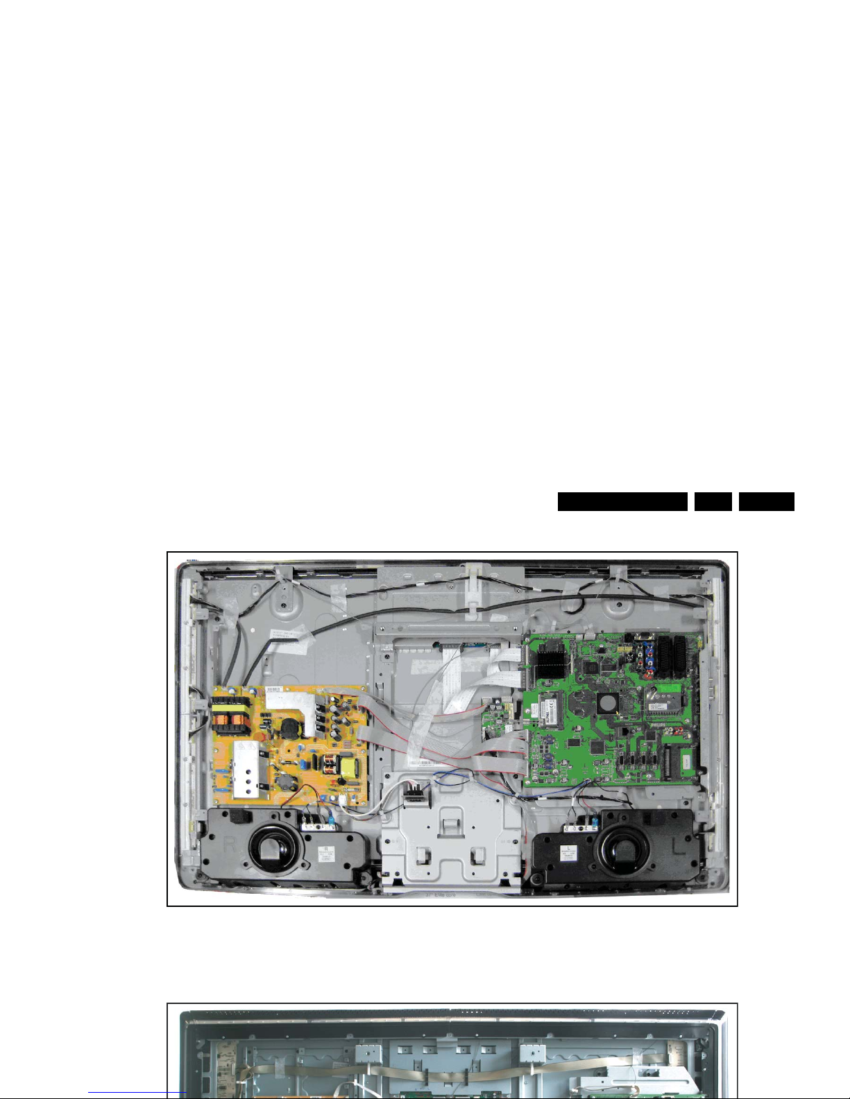
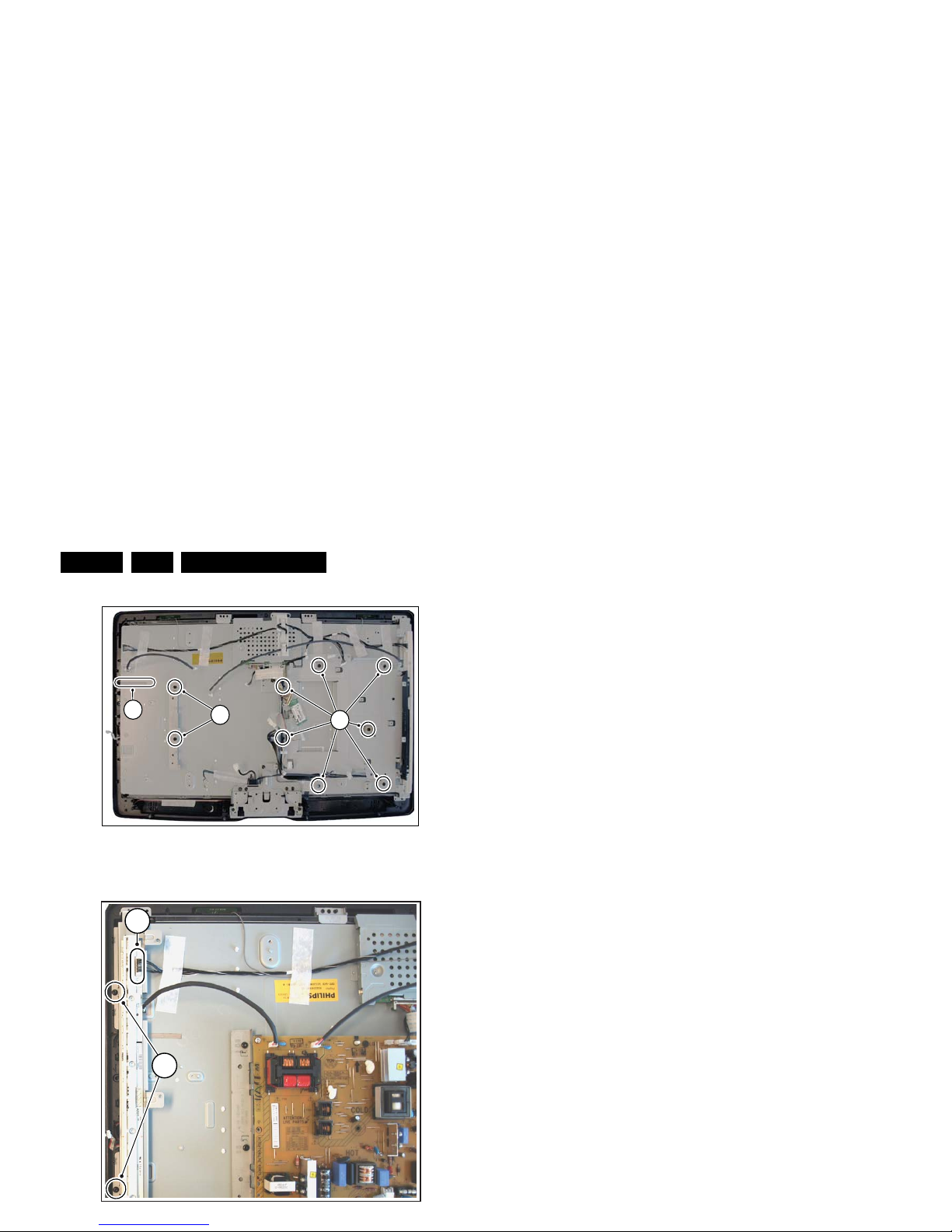
2.4 Chassis Overview
Refer to chapter Block Diagrams for PWB/CBA locations.
19
1
18 2
E_06532_017.eps
250505

Precautions, Notes, and Abbreviation List
EN 6 Q549.2E LA3.
3. Precautions, Notes, and Abbreviation List
Index of this chapter:
3.1 Safety Instructions
3.2 Warnings
3.3 Notes
3.4 Abbreviation List
3.1 Safety Instructions
Safety regulations require the following during a repair:
• Connect the set to the Mains/AC Power via an isolation
transformer (> 800 VA).
• Replace safety components, indicated by the symbol h,
only by components identical to the original ones. Any
other component substitution (other than original type) may
increase risk of fire or electrical shock hazard. Of de set
ontploft!
Safety regulations require that after a repair, the set must be
returned in its original condition. Pay in particular attention to
the following points:
• Route the wire trees correctly and fix them with the
mounted cable clamps.
• Check the insulation of the Mains/AC Power lead for
external damage.
• Check the strain relief of the Mains/AC Power cord for
proper function.
• Check the electrical DC resistance between the Mains/AC
Power plug and the secondary side (only for sets that have
a Mains/AC Power isolated power supply):
1. Unplug the Mains/AC Power cord and connect a wire
between the two pins of the Mains/AC Power plug.
2. Set the Mains/AC Power switch to the “on” position
(keep the Mains/AC Power cord unplugged!).
3. Measure the resistance value between the pins of the
Mains/AC Power plug and the metal shielding of the
tuner or the aerial connection on the set. The reading
should be between 4.5 MΩ and 12 MΩ.
4. Switch “off” the set, and remove the wire between the
two pins of the Mains/AC Power plug.
• Check the cabinet for defects, to prevent touching of any
picture carrier at 475.25 MHz for PAL, or 61.25 MHz for
NTSC (channel 3).
• Where necessary, measure the waveforms and voltages
with (D) and without (E) aerial signal. Measure the
voltages in the power supply section both in normal
operation (G) and in stand-by (F). These values are
indicated by means of the appropriate symbols.
3.3.2 Schematic Notes
• All resistor values are in ohms, and the value multiplier is
often used to indicate the decimal point location (e.g. 2K2
indicates 2.2 kΩ).
• Resistor values with no multiplier may be indicated with
either an “E” or an “R” (e.g. 220E or 220R indicates 220 Ω).
• All capacitor values are given in micro-farads (μ=× 10
-6
),
nano-farads (n =× 10
-9
), or pico-farads (p =× 10
-12
).
• Capacitor values may also use the value multiplier as the
decimal point indication (e.g. 2p2 indicates 2.2 pF).
• An “asterisk” (*) indicates component usage varies. Refer
to the diversity tables for the correct values.
• The correct component values are listed on the Philips
Spare Parts Web Portal.
3.3.3 Spare Parts
For the latest spare part overview, consult your Philips Spare
Part web portal.
3.3.4 BGA (Ball Grid Array) ICs
Introduction
For more information on how to handle BGA devices, visit this
URL: http://www.atyourservice-magazine.com
. Select
“Magazine”, then go to “Repair downloads”. Here you will find
Information on how to deal with BGA-ICs.
BGA Temperature Profiles
For BGA-ICs, you must use the correct temperature-profile.

Precautions, Notes, and Abbreviation List
EN 7Q549.2E LA 3.
3.3.6 Alternative BOM identification
It should be noted that on the European Service website,
“Alternative BOM” is referred to as “Design variant”.
The third digit in the serial number (example:
AG2B0335000001) indicates the number of the alternative
B.O.M. (Bill Of Materials) that has been used for producing the
specific TV set. In general, it is possible that the same TV
model on the market is produced with e.g. two different types
of displays, coming from two different suppliers. This will then
result in sets which have the same CTN (Commercial Type
Number; e.g. 28PW9515/12) but which have a different B.O.M.
number.
By looking at the third digit of the serial number, one can
identify which B.O.M. is used for the TV set he is working with.
If the third digit of the serial number contains the number “1”
(example: AG1B033500001), then the TV set has been
manufactured according to B.O.M. number 1. If the third digit is
a “2” (example: AG2B0335000001), then the set has been
produced according to B.O.M. no. 2. This is important for
ordering the correct spare parts!
For the third digit, the numbers 1...9 and the characters A...Z
can be used, so in total: 9 plus 26= 35 different B.O.M.s can be
indicated by the third digit of the serial number.
Identification: The bottom line of a type plate gives a 14-digit
serial number. Digits 1 and 2 refer to the production centre (e.g.
AG is Bruges), digit 3 refers to the B.O.M. code, digit 4 refers
to the Service version change code, digits 5 and 6 refer to the
production year, and digits 7 and 8 refer to production week (in
example below it is 2006 week 17). The 6 last digits contain the
serial number.
3.4 Abbreviation List
0/6/12 SCART switch control signal on A/V
board. 0 = loop through (AUX to TV),
6 = play 16 : 9 format, 12 = play 4 : 3
format
AARA Automatic Aspect Ratio Adaptation:
algorithm that adapts aspect ratio to
remove horizontal black bars; keeps
the original aspect ratio
ACI Automatic Channel Installation:
algorithm that installs TV channels
directly from a cable network by
means of a predefined TXT page
ADC Analogue to Digital Converter
AFC Automatic Frequency Control: control
signal used to tune to the correct
frequency
AGC Automatic Gain Control: algorithm that
controls the video input of the feature
box
AM Amplitude Modulation
AP Asia Pacific
AR Aspect Ratio: 4 by 3 or 16 by 9
ASF Auto Screen Fit: algorithm that adapts
aspect ratio to remove horizontal black
bars without discarding video
information
ATSC Advanced Television Systems
Committee, the digital TV standard in
the USA
ATV See Auto TV
Auto TV A hardware and software control
system that measures picture content,
and adapts image parameters in a
dynamic way
AV External Audio Video
AVC Audio Video Controller
AVIP Audio Video Input Processor
B/G Monochrome TV system. Sound
carrier distance is 5.5 MHz
BLR Board-Level Repair
BTSC Broadcast Television Standard
10000_024_090121.eps
090121
MODEL :
PROD.NO:
~
S
32PF9968/10
MADE IN BELGIUM
220-240V 50/60Hz
128W
AG 1A0617 000001
VHF+S+H+UHF
BJ3.0E LA

Precautions, Notes, and Abbreviation List
EN 8 Q549.2E LA3.
DNR Digital Noise Reduction: noise
reduction feature of the set
DRAM Dynamic RAM
DRM Digital Rights Management
DSP Digital Signal Processing
DST Dealer Service Tool: special remote
control designed for service
technicians
DTCP Digital Transmission Content
Protection; A protocol for protecting
digital audio/video content that is
traversing a high speed serial bus,
such as IEEE-1394
DVB-C Digital Video Broadcast - Cable
DVB-T Digital Video Broadcast - Terrestrial
DVD Digital Versatile Disc
DVI(-d) Digital Visual Interface (d= digital only)
E-DDC Enhanced Display Data Channel
(VESA standard for communication
channel and display). Using E-DDC,
the video source can read the EDID
information form the display.
EDID Extended Display Identification Data
(VESA standard)
EEPROM Electrically Erasable and
Programmable Read Only Memory
EMI Electro Magnetic Interference
EPLD Erasable Programmable Logic Device
EU Europe
EXT EXTernal (source), entering the set by
SCART or by cinches (jacks)
FDS Full Dual Screen (same as FDW)
FDW Full Dual Window (same as FDS)
FLASH FLASH memory
FM Field Memory or Frequency
Modulation
FPGA Field-Programmable Gate Array
FTV Flat TeleVision
Gb/s Giga bits per second
G-TXT Green TeleteXT
H H_sync to the module
HD High Definition
HDD Hard Disk Drive
HDCP High-bandwidth Digital Content
uses 8 bit or 10 bit data words, and has
a maximum data rate of 270 Mbit/s,
with a minimum bandwidth of 135
MHz.
ITV Institutional TeleVision; TV sets for
hotels, hospitals etc.
LS Last Status; The settings last chosen
by the customer and read and stored
in RAM or in the NVM. They are called
at start-up of the set to configure it
according to the customer's
preferences
LATAM Latin America
LCD Liquid Crystal Display
LED Light Emitting Diode
L/L' Monochrome TV system. Sound
carrier distance is 6.5 MHz. L' is Band
I, L is all bands except for Band I
LPL LG.Philips LCD (supplier)
LS Loudspeaker
LVDS Low Voltage Differential Signalling
Mbps Mega bits per second
M/N Monochrome TV system. Sound
carrier distance is 4.5 MHz
MIPS Microprocessor without Interlocked
Pipeline-Stages; A RISC-based
microprocessor
MOP Matrix Output Processor
MOSFET Metal Oxide Silicon Field Effect
Transistor, switching device
MPEG Motion Pictures Experts Group
MPIF Multi Platform InterFace
MUTE MUTE Line
NC Not Connected
NICAM Near Instantaneous Compounded
Audio Multiplexing. This is a digital
sound system, mainly used in Europe.
NTC Negative Temperature Coefficient,
non-linear resistor
NTSC National Television Standard
Committee. Color system mainly used
in North America and Japan. Color
carrier NTSC M/N= 3.579545 MHz,
NTSC 4.43= 4.433619 MHz (this is a

Precautions, Notes, and Abbreviation List
EN 9Q549.2E LA 3.
PWM Pulse Width Modulation
QRC Quasi Resonant Converter
QTNR Quality Temporal Noise Reduction
QVCP Quality Video Composition Processor
RAM Random Access Memory
RGB Red, Green, and Blue. The primary
color signals for TV. By mixing levels
of R, G, and B, all colors (Y/C) are
reproduced.
RC Remote Control
RC5 / RC6 Signal protocol from the remote
control receiver
RESET RESET signal
ROM Read Only Memory
RSDS Reduced Swing Differential Signalling
data interface
R-TXT Red TeleteXT
SAM Service Alignment Mode
S/C Short Circuit
SCART Syndicat des Constructeurs
d'Appareils Radiorécepteurs et
Téléviseurs
SCL Serial Clock I
2
C
SCL-F CLock Signal on Fast I
2
C bus
SD Standard Definition
SDA Serial Data I
2
C
SDA-F DAta Signal on Fast I
2
C bus
SDI Serial Digital Interface, see “ITU-656”
SDRAM Synchronous DRAM
SECAM SEequence Couleur Avec Mémoire.
Color system mainly used in France
and East Europe. Color carriers=
4.406250 MHz and 4.250000 MHz
SIF Sound Intermediate Frequency
SMPS Switched Mode Power Supply
SoC System on Chip
SOG Sync On Green
SOPS Self Oscillating Power Supply
SPI Serial Peripheral Interface bus; a 4-
wire synchronous serial data link
standard
S/PDIF Sony Philips Digital InterFace
SRAM Static RAM
SRP Service Reference Protocol
Y Luminance signal
Y/C Luminance (Y) and Chrominance (C)
signal
YPbPr Component video. Luminance and
scaled color difference signals (B-Y
and R-Y)
YUV Component video
Mechanical Instructions
EN 10 Q549.2E LA4.
4. Mechanical Instructions
Index of this chapter:
4.1 Cable Dressing and Taping
4.2 Service Positions
4.3 Assy/Panel Removal
4.4 Set Re-assembly
Notes:
• Figures below can deviate slightly from the actual situation,
due to the different set executions.
4.1 Cable Dressing and Taping
Mechanical Instructions
EN 11Q549.2E LA 4.
Figure 4-2 Cable dressing 37"
18310_211_090318.eps
090318
Mechanical Instructions
EN 12 Q549.2E LA4.
4.2 Service Positions
For easy servicing of this set, there are a few possibilities
created:
• The buffers from the packaging.
• Foam bars (created for Service).
4.2.1 Foam Bars
Figure 4-4 Foam bars
The foam bars (order code 3122 785 90580 for two pieces) can
be used for all types and sizes of Flat TVs.
See Figure 4-4
for details. Sets with a display of 42" and larger,
require four foam bars [1]. Ensure that the foam bars are
always supporting the cabinet and never only the display.
Caution: Failure to follow these guidelines can seriously
damage the display!
By laying the TV face down on the (ESD protective) foam bars,
4.3.3 Ambi Light
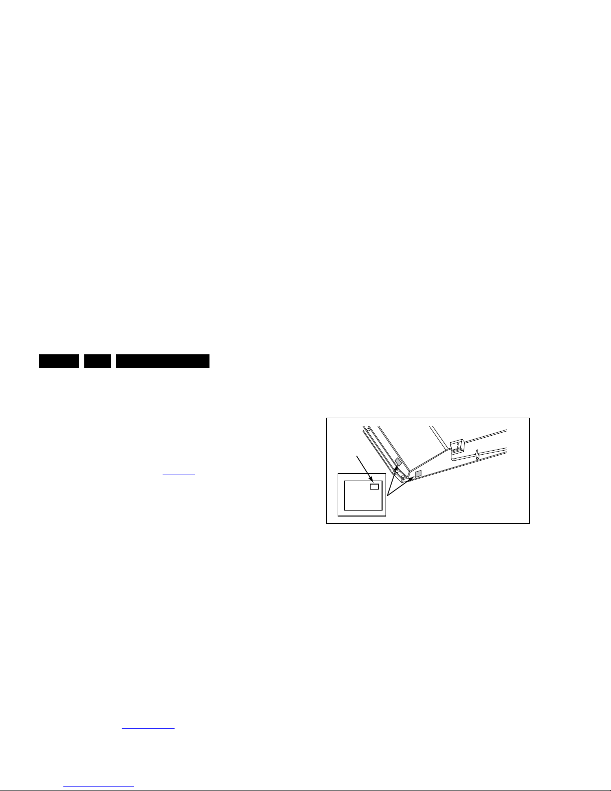
Each Ambi Light unit is mounted on a subframe. Refer to
Figure 4-5
for details.
Figure 4-5 Ambi Light unit
1. Remove the Ambi Light cover [1].
2. Unplug the connector(s).
3. The PWB can now be taken from the subframe.
When defective, replace the whole unit.
Note: the screws that secure the AmbiLight units are longer
than the other screws.
E_06532_018.eps
171106
1
Required for sets
42"
1
18310_212_090318.eps
090319
1
Mechanical Instructions
EN 13Q549.2E LA 4.
1. Remove the Main Supply Panel as earlier described.
2. Remove the stand [1] and its subframe [2].
3. Now you gain access the IR & LED board.
When defective, replace the whole unit.
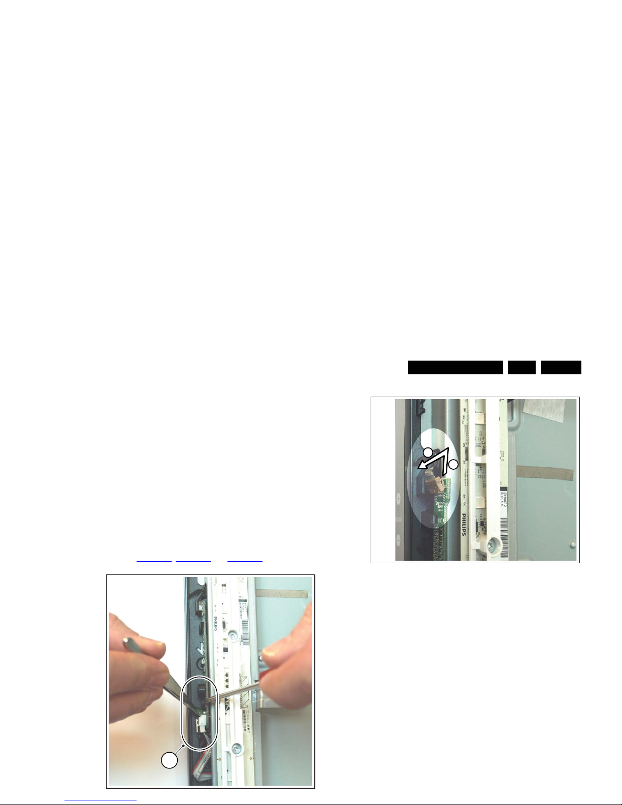
4.3.6 Piezo Touch Control Panel
The flexfoil between Piezo Flexfoil Assy (mounted on the
plastic rim of the set), and the PWB as described below, is
extremely vulnerable. Do not pull hard at the PWB or
flexfoil.
Once the flexfoil has been damaged, the entire plastic rim
of the set (with the touch-control pads) has to be swapped!
The Piezo Touch Control Panel PWB contains ESD sensitive
components, implying that necessary industrial ESD
precautions must be taken during removing or remounting.
Refer to Figure 4-7
, Figure 4-8 and Figure 4-9 for details.
Figure 4-9 Piezo Touch Control Panel -3-
1. To unplug the flexfoil connector, first the outer part of the
connector has to be moved upwards [3], before this part
can be turned sidewards [4] as shown in the picture. Now
the flexfoil can be removed from the connector and the
PWB can be taken out of the set.
When defective, replace the whole unit.
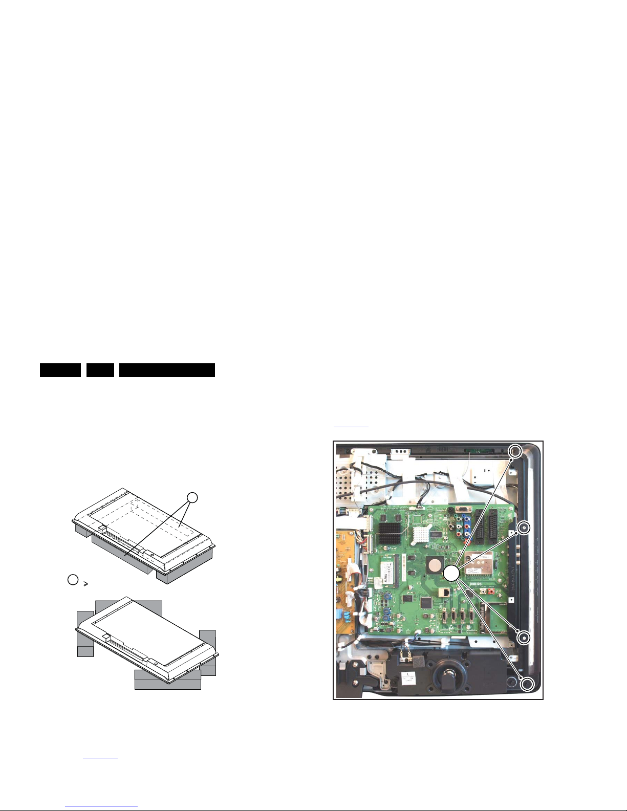
4.3.7 Small Signal Board (SSB)
Caution: It is mandatory to remount screws at their original
position during re-assembly. Failure to do so may result in
damaging the SSB.
1. Remove the Wi-Fi module that is mounted on the SSB.
2. Unplug all connectors.
3. Remove the screws that secure the board.
4. The SSB can now be taken out of the set.
4.3.8 LCD Panel
18310_214_090318.eps
090319
1
18310_215_090318.eps
090319
3
4
Mechanical Instructions
EN 14 Q549.2E LA4.
Figure 4-10 LCD Panel -1-
18310_217_090318.eps
090320
1
4
1
18310_218_090318.eps
090319
3
2

Service Modes, Error Codes, and Fault Finding
EN 15Q549.2E LA 5.
5. Service Modes, Error Codes, and Fault Finding
Index of this chapter:
5.1 Test Points
5.2 Service Modes
5.3 Stepwise Start-up
5.4 Service Tools
5.5 Error Codes
5.6 The Blinking LED Procedure
5.7 Protections
5.8 Fault Finding and Repair Tips
5.9 Software Upgrading
5.1 Test Points
As most signals are digital, it will be difficult to measure
waveforms with a standard oscilloscope. However, several key
ICs are capable of generating test patterns, which can be
controlled via ComPair. In this way it is possible to determine
which part is defective.
Perform measurements under the following conditions:
• Service Default Mode.
• Video: Colour bar signal.
• Audio: 3 kHz left, 1 kHz right.
5.2 Service Modes
Service Default mode (SDM) and Service Alignment Mode
(SAM) offers several features for the service technician, while
the Customer Service Mode (CSM) is used for communication
between the call centre and the customer.
This chassis also offers the option of using ComPair, a
hardware interface between a computer and the TV chassis. It
offers the abilities of structured troubleshooting, error code
reading, and software version read-out for all chassis.
(see also section “5.4.1 ComPair
”).
Note: For the new model range, a new remote control (RC) is
• All service-unfriendly modes (if present) are disabled, like:
– (Sleep) timer.
– Child/parental lock.
– Picture mute (blue mute or black mute).
– Automatic volume levelling (AVL).
– Skip/blank of non-favourite pre-sets.
How to Activate SDM
For this chassis there are two kinds of SDM: an analog SDM
and a digital SDM. Tuning will happen according Table 5-1
.
• Analog SDM: use the standard RC-transmitter and key in
the code “062596”, directly followed by the “MENU” (or
HOME) button.
Note: It is possible that, together with the SDM, the main
menu will appear. To switch it “off”, push the “MENU”(or
HOME) button again.
• Digital SDM: use the standard RC-transmitter and key in
the code “062593”, directly followed by the “MENU” (or
HOME) button.
Note: It is possible that, together with the SDM, the main
menu will appear. To switch it “off”, push the “MENU” (or
HOME) button again.
• Analog SDM can also be activated by grounding for a
moment the solder pad on the SSB, with the indication
“SDM” (see Service mode pad
).
SDM
Service Modes, Error Codes, and Fault Finding
EN 16 Q549.2E LA5.
• To view operation hours.
• To display (or clear) the error code buffer.
How to Activate SAM
Via a standard RC transmitter: Key in the code “062596”
directly followed by the “INFO” button. After activating SAM
with this method a service warning will appear on the screen,
continue by pressing the “OK” button on the RC.
Contents of SAM (see also Table 6-4
)
• Hardware Info.
– A. SW Version. Displays the software version of the
main software (example: Q5492-1.2.3.4 =
AAAAB_X.Y.W.Z).
• AAAA= the chassis name.
• B= the SW branch version. This is a sequential
number (this is no longer the region indication, as
the software is now multi-region).
• X.Y.W.Z= the software version, where X is the
main version number (different numbers are not
compatible with one another) and Y.W.Z is the sub
version number (a higher number is always
compatible with a lower number).
– B. STBY PROC Version. Displays the software
version of the stand-by processor.
– C. Production Code. Displays the production code of
the TV, this is the serial number as printed on the back
of the TV set. Note that if an NVM is replaced or is
initialized after corruption, this production code has to
be re-written to NVM. ComPair will foresee in a
possibility to do this.
• Operation Hours. Displays the accumulated total of
operation hours (not the stand-by hours). Every time the
TV is switched “on/off”, 0.5 hours is added to this number.
• Errors (followed by maximum 10 errors). The most recent
error is displayed at the upper left (for an error explanation
see section “5.5 Error Codes
”).
• Reset Error Buffer. When “cursor right” (or the “OK
button) is pressed and then the “OK” button is pressed, the
error buffer is reset.
• Alignments. This will activate the “ALIGNMENTS” submenu. See Chapter 6. Alignments.
• Dealer Options. Extra features for the dealers.
TV will go to the Stand-by mode. If the NVM was corrupted or
empty before this action, it will be initialized first (loaded with
default values). This initializing can take up to 20 seconds.
Figure 5-2 Location of Display Option Code sticker
• Store - go right. All options and alignments are stored
when pressing “cursor right” (or the “OK” button) and then
the “OK”-button.
• SW Maintenance.
– SW Events. Not useful for Service purposes. In case
of specific software problems, the development
department can ask for this info.
– HW Events. Not useful for Service purposes. In case
of specific software problems, the development
department can ask for this info.
• Operation hours display. Displays the accumulated total
of display operation hours. So, this one keeps up the
lifetime of the display itself, mainly to compensate the
degeneration behaviour.
• Test settings. For development purposes only.
• Development file versions. Not useful for Service
purposes, this information is only used by the development
department.
• Upload to USB. To upload several settings from the TV to
an USB stick, which is connected to the SSB. The items are
“Channel list”, “Personal settings”, “Option codes”,
“Display-related alignments” and “History list”. First a
directory “repair\” has to be created in the root of the
USB stick. To upload the settings select each item
PHILIPS
MODEL:
32PF9968/10
PROD.SERIAL NO:
AG 1A0620 000001
040
39mm
27mm
(CTN Sticker)
Display Option
Code
E_06532_038.eps
240108

Service Modes, Error Codes, and Fault Finding
EN 17Q549.2E LA 5.
• With the “OK” key, it is possible to activate the selected
action.
How to Exit SAM
Use one of the following methods:
• Switch the TV set to STAND-BY via the RC-transmitter.
• Via a standard RC-transmitter, key in “00” sequence, or
select the “BACK” key.
5.2.3 Customer Service Mode (CSM)
Purpose
When a customer is having problems with his TV-set, he can
call his dealer or the Customer Helpdesk. The service
technician can then ask the customer to activate the CSM, in
order to identify the status of the set. Now, the service
technician can judge the severity of the complaint. In many
cases, he can advise the customer how to solve the problem,
or he can decide if it is necessary to visit the customer.
The CSM is a read only mode; therefore, modifications in this
mode are not possible.
When in this chassis CSM is activated, a testpattern will be
displayed during 5 seconds (1 second Blue, 1 second Green
and 1 second Red, then again 1 second Blue and 1 second
Green). This test pattern is generated by the PNX5100. So if
this test pattern is shown, it could be determined that the back
end video chain (PNX5100, LVDS, and display) of the SSB is
working.
When CSM is activated and there is a USB stick connected to
the TV, the software will dump the complete CSM content to the
USB stick. The file (Csm.txt) will be saved in the root of the USB
stick. This info can be handy if no information is displayed.
Also when CSM is activated, the LAYER 1 error is displayed via
blinking LED. Only the latest error is displayed. (see also
section 5.5 Error Codes
).
How to Activate CSM
Key in the code “123654” via the standard RC transmitter.
Note: Activation of the CSM is only possible if there is no (user)
menu on the screen!
NVM. ComPair will foresee in a possibility to do this. This
identification number is the 12nc number of the SSB.
• 12NC display. Shows the 12NC of the display.
• 12NC supply. Shows the 12NC of the supply.
• 12NC “fan board”. Shows the 12NC of the “fan board”module (for sets with LED backlight)
• 12NC “LED Dimming Panel”. Shows the 12NC of the
LED dimming Panel (for sets with LED backlight).
Software versions
• Current main SW. Displays the built-in main software
version. In case of field problems related to software,
software can be upgraded. As this software is consumer
upgradeable, it will also be published on the Internet.
Example: Q5492_1.2.3.4
• Standby SW. Displays the built-in stand-by processor
software version. Upgrading this software will be possible
via ComPair or via USB (see section 5.9 Software
Upgrading).
Example: STDBY_88.68.1.2.
• MOP ambient light SW. Displays the MOP ambient light
EPLD SW.
• LED Dimming SW. Displays the LED Dimming EPLD SWversion (for sets with LED backlight).
• Local contrast SW. Displays the MOP local contrast SWversion.
Quality items
• Signal quality. Poor / average /good
• Child lock. Not active / active. This is a combined item for
locks. If any lock (Preset lock, child lock, lock after or
parental lock) is active, the item shall show “active”.
• HDMI HDCP key. Indicates if the HDMI keys (or HDCP
keys) are valid or not. In case these keys are not valid and
the customer wants to make use of the HDMI functionality,
the SSB has to be replaced.
• Ethernet MAC address. Displays the MAC address
present in the SSB.
• Wireless MAC address. Displays the wireless MAC
address to support the Wi-Fi functionality.
• BDS key. Indicates if the “BDS level 1” key is valid or not.
• CI slot present. If the common interface module is
detected the result will be “YES” or “NO”.
Service Modes, Error Codes, and Fault Finding
EN 18 Q549.2E LA5.
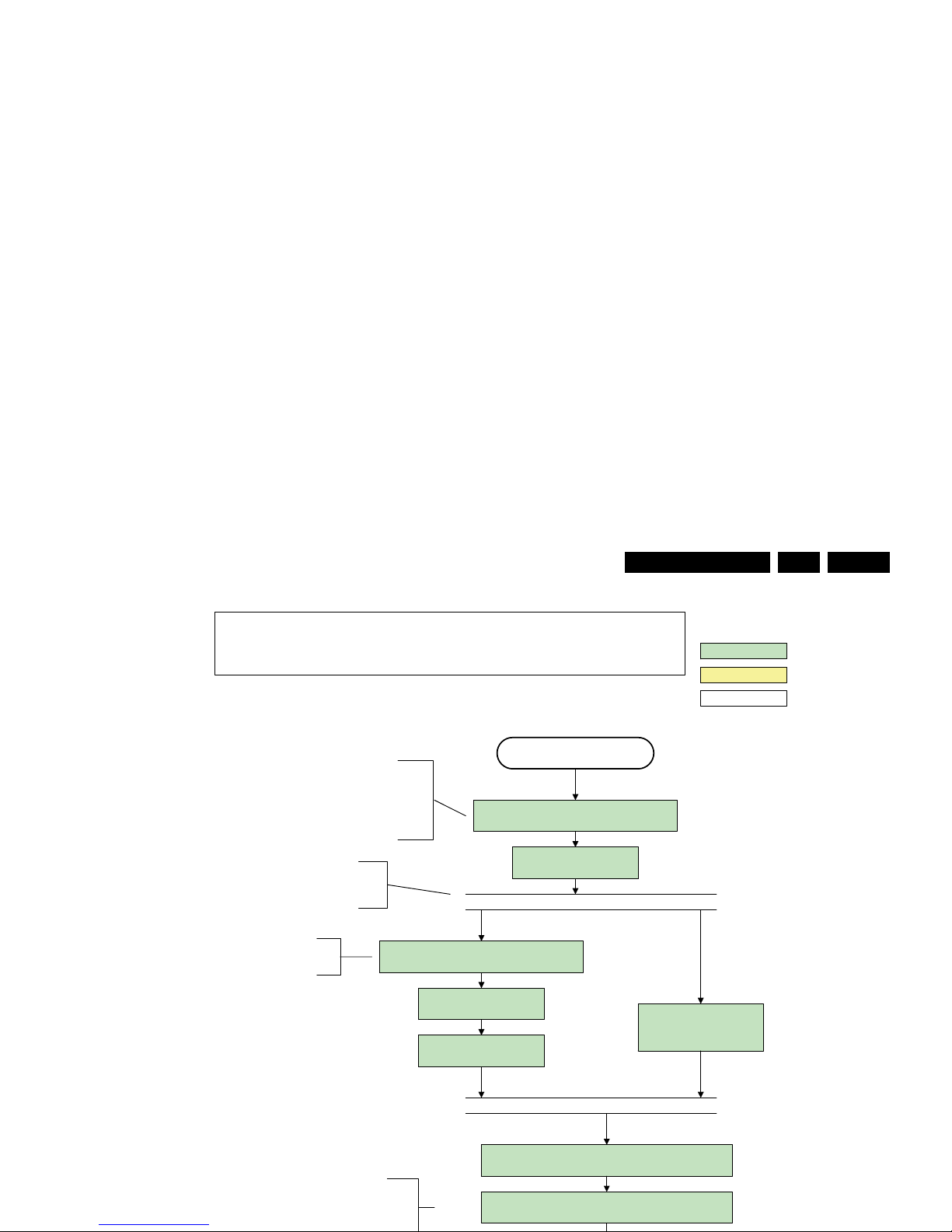
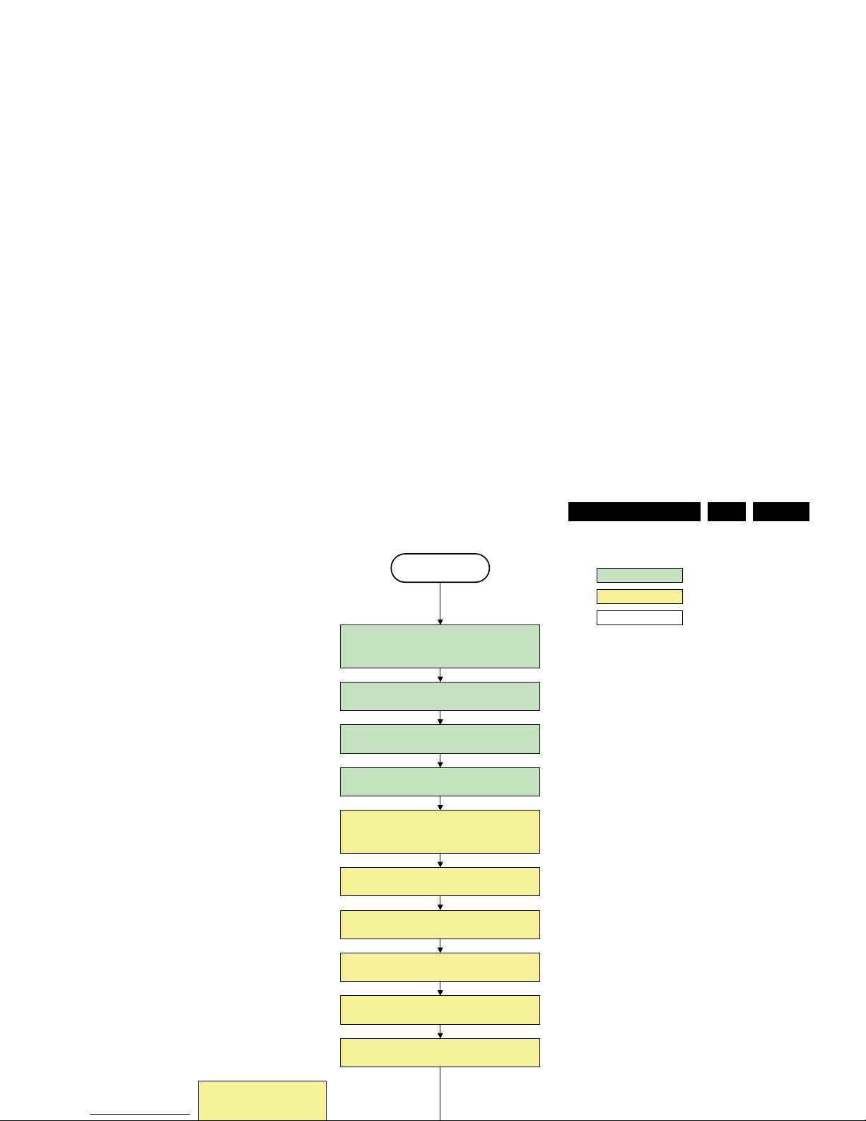
5.3 Stepwise Start-up
When the TV is in a protection state due to an error detected by
stand-by software (error blinking is displayed) and SDM is
activated via shortcutting the pins on the SSB, the TV starts up
until it reaches the situation just before protection. So, this is a
kind of automatic stepwise start-up. In combination with the
start-up diagrams below, you can see which supplies are
present at a certain moment. Important to know is, that if e.g.
the 3V3 detection fails and thus error layer 2 = 18 is blinking
while the TV is restarted via SDM, the Stand-by Processor will
enable the 3V3, but the TV set will not go to protection now.
The TV will stay in this situation until it is reset (Mains/AC
Power supply interrupted). Caution: in case the start-up in this
mode with a faulty FET 7U08 is done, you can destroy all IC’s
supplied by the +3V3, due to overvoltage (12V on 3V3-line). It
is recommended to measure first the FET 7U08 or others
FET’s on shortcircuit before activating SDM via the service
pads.
The abbreviations “SP” and “MP” in the figures stand for:
• SP: protection or error detected by the Stand-by
Processor.
• MP: protection or error detected by the MIPS Main
Processor.
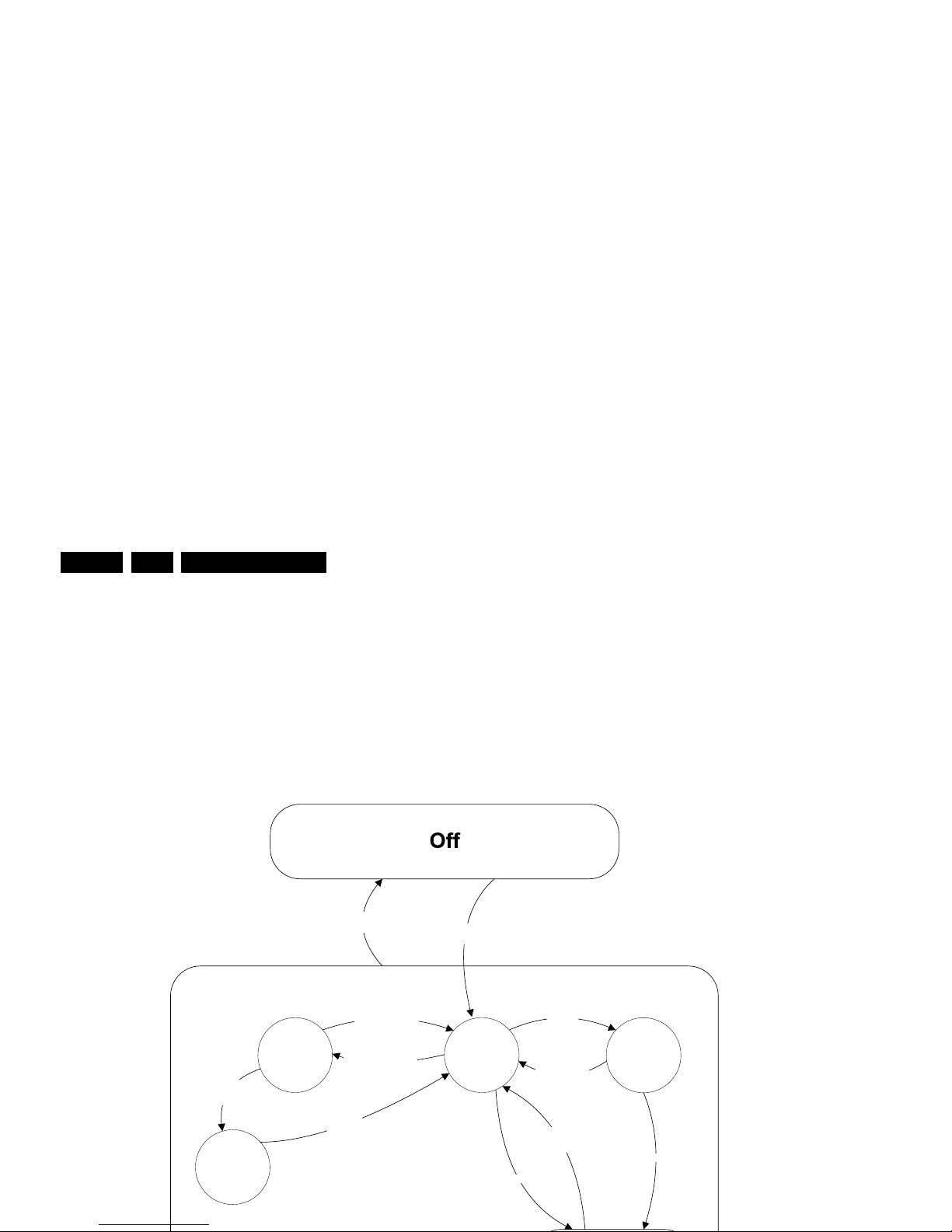
Active
Semi
St by
St by
Mains
on
Mains
off
GoToProtection
-WakeUp requested
-Acquisition needed
-No data Acquisition
required
-tact SW pushed
-last status is hibernate
after mains ON
- St by requested
-tact SW pushed
WakeUp
requested
WakeUp
requested
(SDM)
GoToProtection
Hibernate
-Tact switch Pushed
-last status is hibernate
after mains ON
Tact switch
pushed
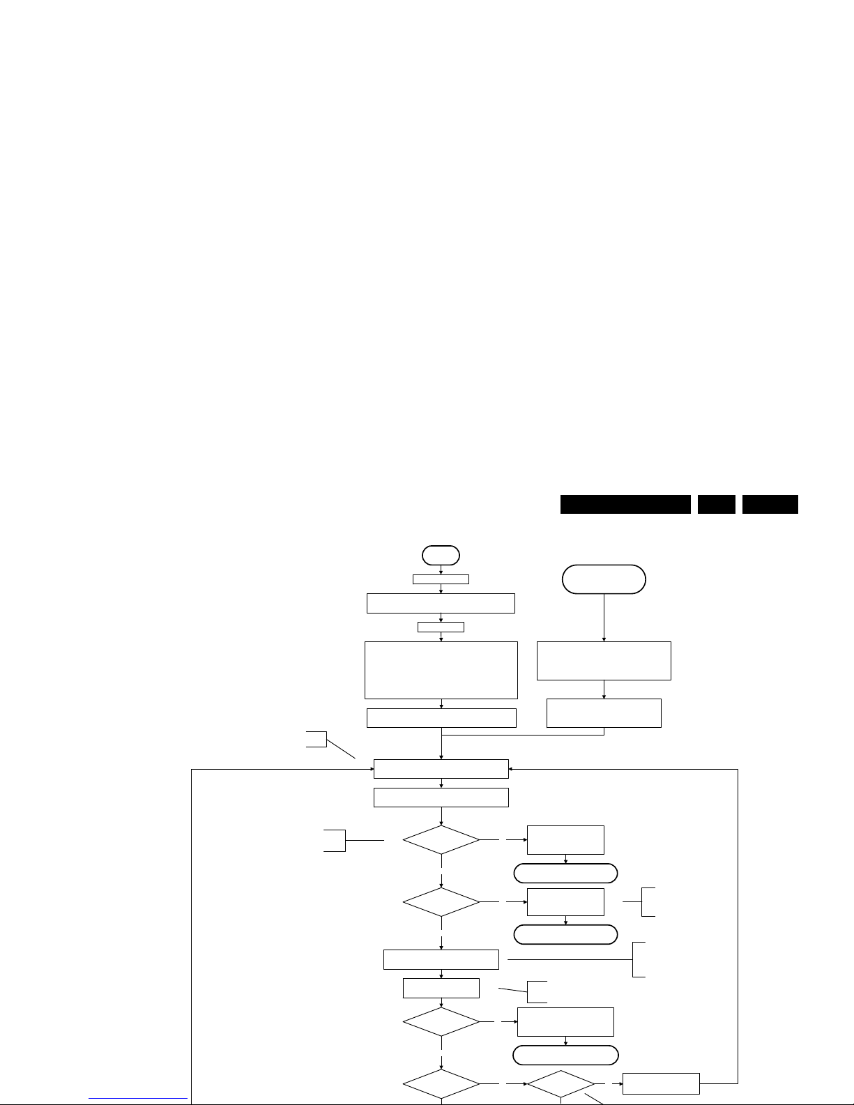
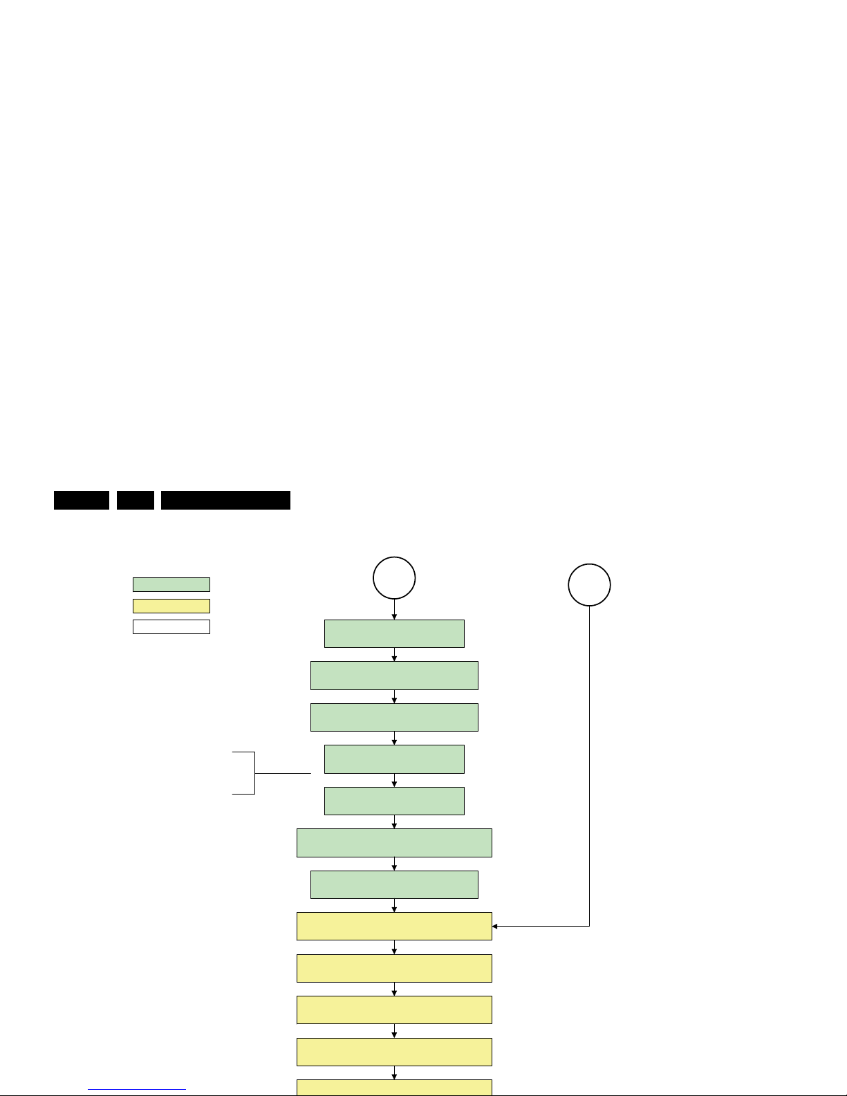
Service Modes, Error Codes, and Fault Finding
EN 19Q549.2E LA 5.
Initialise I/O pins of the st-by µP:
- Switch reset-AVCLOW (reset state)
- Switch WP-NandFlash LOW (protected)
- Switch reset-system LOW (reset state)
- Switch reset-5100 LOW (reset state)
- Switch reset-Ethernet LOW (reset state)
- Switch reset-ST7100 LOW (reset state)
- keep reset-NVM high, Audio-reset and Audio-Mute-Up HIGH
Off
Standby Supply starts running.
All standby supply voltages become available .
st-by µP resets
Stand by or
Protection
Mains is applie d
- Switch Audio-Reset high.
It is low in the standby mode if the standby
mode lasted longer than 10s.
start keyboard scanning, RC detection. Wake up reasons are
off.
If the protection state was left by short circuiting the
SDM pins, detection of a protection condition during
startup will stall the startup. Protection conditions in a
playing set will be ignored. The protection mode will
not be entered.
+12V, +/-12Vs, AL and Bolt-on power
is switched on, followed by the +1V2 DCDC converter
No
Detect-1 I/O line
High?
Switch ON Platform and display supply by switching
LOW the Standby line.
This enables the +3V3 and
+5V converter. As a result,
also +5V-tuner, +2V5, +1V8PNX8541 and +1V8-PNX5100
become available.
yes
Enable the DCDC converter for +3V3 and
+5V. (EN ABLE-3V3)
Important remark; the appearance of the +12V
will start the +1V2 DCDC converter automatically
No
Yes
Supply-fault I/O
High?
The supply-fault line is a
combination of the DCDC
converters and the audio
protection line.
1V2 DCDC or class D error:
Layer1: 2
Layer2: 19
Enter protection
No
Detect2 high received
within 1 second?
Power-OK err or:
Layer1: 3
Layer2: 16
Enter protection
Yes
No
Supply-fault I/O
High?
3V3 / 5V DCDC or class D error:
Layer1: 2
Layer2: 11
Enter protection
Wait 50ms
Delay of 50ms needed because of the latency of the detect-1 circuit.
This delay is also needed for the PNX5100. The reset of the
PNX5100 should only be released 10ms after powering the IC.
Detect2 should be polled on the standard 40ms
interval and startup should be continued when
detect2 becomes high.
No
Detect -2 I/O line
High?
Disable 3V3, swit ch standby
line high and wait 4 seconds
Service Modes, Error Codes, and Fault Finding
EN 20 Q549.2E LA5.
Yes
MIPS reads the wake up reason
from standby µP.
initialize tuner, Master IF and channel
3-th try?
No
Blink Code as
error code
Bootscript ready
in 1250 ms?
Yes
No
Enable Alive check mechanism
Wait until AVC starts to
communicate
SW initializatio n
succeeded
within 20s?
No
Switch Standby
I/O line high.
RPC start (comm. protocol)
Set I²C slave address
of Standby µP to (60h)
Yes
Disable all supply related protections and
switch off the +3V3 +5V DC/DC converter.
switch off the remaining DC/DC
converters
Wait 5ms
Switch AVC PNX854 1
in reset (active low )
Wait 10ms
Switch the NVM reset
line HIGH.
Flash to Ram
image transfer succeeded
within 30s?
No
Yes
Code =
Layer1: 2
Layer2: 53
Code =
Layer1: 2
Layer2: 15
Timing need to be updated if
more mature info is available.
Timing needs to
be updated if more
matur e info is
available.
Timing needs to be
updated if more
matur e info is
available.
Downloaded
successfully ?
Download firmware into the channel
decoder
Third try? No
No
Yes
Log channel decoder error:
Layer1: 2
Yes
Initialize audio
Enter protection
Release reset MPEG4 module:
BOLT-ON-IO: High
MPEG4 module will start booting
autonomously.
Wait 3000 ms
Start alive IIC polling
mechanism
POR polling p ositive ?
yes
No
Log SW event:
STi7100PorFailure
Wait 200 ms
POR polling positive?yes
No
bootSTi7100PorFailure:
Log HW error
Layer1: 2
Layer2: 38
and generate cold boot
Alive
polling
Log SW event
STi7100AliveFailedError
and generate fast cold reboot
eventually followed by a cold
reboot.
NOK
Reset-system is switched HIGH by the
AVC at the end of the bootscript
AVC releases Reset-Ethernet when the
end of the AVC boot-script is detected
This cannot be done through the bootscript,
the I/O is on the standby µP
Reset- system is connected to USB
From I_17660_125a.eps From I_17660_125a.eps
-reset,
4to1HDMI Mux and channel decoder.
Reset-Audio and Audio-Mute-Up are
switched by MIPS code later on in the
startup process
Reset-syst em is switched HIGH by the
AVC at the end of the bootscript
AVC releases Reset-Ethernet when the
end of the AVC boot-script is detected
Reset-Audio and Audio-Mute-Up are
switched by MIPS code later on in the
startup process
Switch on the display in case of a LED backlight
display by sending the TurnOnDisplay(1) (I²C)
command to the PNX5100
In case of a LED backlight display, a LED DIM panel is
present which is fed by the Vdisplay. To power the LED DIM
Panel, the Vdisplay switch driven by the PNX5100 must be
closed. The display startup sequence is taken care of by the
LED DIM panel.
Service Modes, Error Codes, and Fault Finding
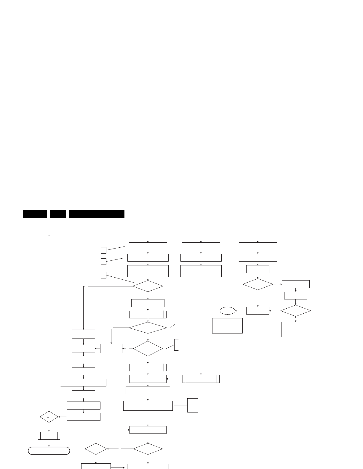
EN 21Q549.2E LA 5.
Semi Standby
action holder: AVC
autonomous action
action holder: St-by
Initialize audio and video
processing IC's and functions
according needed use case.
Assert RGB video blanking
and audio mute
Wait until previous on-state is left more than 2
seconds ago. (to prevent LCD display problems)
The assumption here is t hat a fast tog gle (<2s)
can only happen during ON-> SEMI ->ON. In
these stat es, th e AVC is still active an d can
provide the 2s delay. If the transition ON-> SEMI-
>STBY -> SEMI -> ON can be made in less th an 2s,
the semi -> stby transition has to be delayed
until the requirement is met.
Switch Audio -Reset low and w ait 5ms
Constraints taken into account:
- Display may only be started when valid LVDS output clock can be delivered by the AVC.
- Between 5 and 50 ms after power is supplied, display should receive valid lvds clock .
- minimum wait time to switch on the lamp after power up is 200ms.
Wait until valid and stable audio and video , corresponding to
the requested output is delivered by the AVC.
The higher level requirement is that audio and
video should be demuted without transient
effects and that the audio should be demuted
maximum 1s before or at the same time as the
CPipe already generates a valid output
clock in t he sem i -standby st ate : display
startup can start immediately when leaving
the semi-standby state.
wait 250ms (min. = 200ms)
Switch on LCD backlight
(Lamp-ON)
Switch on the display by sending the
TurnOnDisplay(1) (I²C) command to the PNX5100
The timings to be used in
combination with the PanelON
comman d for th is specific d isplay
Service Modes, Error Codes, and Fault Finding
EN 22 Q549.2E LA5.
Semi Standby
action holder: AVC
autonomous action
action holder: St-by
Initialize audio and video
processing IC's and functions
according needed use case.
Assert RGB video blanking
and audio mute
Wait until previous on-state is left more than 2
seconds ago. (to prevent LCD display problems)
The assumption here is t hat a fast tog gle (<2s)
can only happen during ON->SEMI ->ON. In
these stat es, th e AVC is still active and can
provide t he 2s delay. If the tran sition ON -> SEMI-
->STBY-> SEMI -> ON can be made in less than 2s,
the semi - > stby transition has to be delayed
until the requirement is met.
Constraints taken into account:
- Display may only be started when valid LVDS output clock can be delivered by the AVC.
- Between 5 and 50 ms after power is supplied, display should receive valid lvds clock .
- minimum wait time to switch on the lamp after power up is 200ms.
- To have a reliable operation of the backlight, the backlight should be driven with a PWM duty cycle of 100%
during the first second. Only after this first one or two seconds, the PWM may be set to the required output level
(Note that the PWM output should be present before the backlight is switched on). To minimize the artefacts, the
picture should only be unblanked after these first seconds.
Wait until valid and stable audio and video , corresponding to the requested
output is delivered by the AVC
AND
[the backlight PWM has been on for 1s (internal inverter LPL displays
CPipe already generates a valid output
clock in t he sem i -standby st ate: displa y
startup can start immediately when leaving
the semi-standby state.
wait 250ms (min. = 200ms)
Switch on L CD backlig ht
(Lamp-ON)
Switch off the dimming backlight feature, set
the BOOST control to nominal and make sure
PWM output is set to 100%
Switch on the display by sending the
TurnOnDisplay(1) (I²C) command to the PNX5100
Service Modes, Error Codes, and Fault Finding
EN 23Q549.2E LA 5.
Semi Standby
action holder: AVC
autonomous action
action holder: St-by
Initialize audio and video
processing IC's and functions
according needed use case.
Assert RGB video blanking
and audio mute
Wait until previous on-state is left more than 2
seconds ago. (to prevent LCD display problems)
The assumption here is that a fast toggle (<2s)
can only happen during ON-> SEMI -> ON. In
these stat es, the A VC is still active and can
provide the 2s delay. If the t ransition ON -> SEMI-
>STBY->SEMI->ON can be made in less t han 2s,
the semi -> stby transition has to be delayed
until the requirement is met.
Switch Audio -Reset low and w ait 5ms
Constraints taken into account:
- Display may only be started when valid LVDS output clock can be delivered by the AVC .
- Between 5 and 50 ms after power is supplied, display should receive valid lvds clock .
- minimum wait time to switch on the lamp after power up is 200ms.
Wait until valid and stable audio and video , corresponding to
the requested output is delivered by the AVC.
The higher level requirement is that audio and
video should be demuted without transient
effects and that the audio should be demuted
maximum 1s before or at the same time as the
unblanking of the video.
Release audio mute and wait 100ms before any other audio
handling is done (e.g. volume change)
CPipe already generates a valid output
clock in t he sem i -standby st ate : display
startup can start immediately when leaving
the semi-standby state.
wait 250ms (min. = 200ms)
TBC in def. spec
Switch on L CD backlig ht
(Lamp-ON)
Switch on the display by sending the OUTPUT-
ENABLE (I²C) command to the LED DIM panel
Service Modes, Error Codes, and Fault Finding
EN 24 Q549.2E LA5.
Semi Standby
Active
action holder: AVC
autonomous action
action holder: St-by
Wait 25 0ms ( min. = 2 00ms)
Mute all sound outputs via softmute
Mute all video outputs
switch off LCD backlight
Force ext audio outputs to ground
(I/O: audio reset)
And wait 5ms
Switch off the display by sending the
TurnOnDisplay(0) (I²C) command to the PNX5100
switch o ff Am bilight
Set main amplifier mute (I/O: audio-mute)
Wait 100ms
Wait until Ambilight has faded out
(fixed wait time of x s)
The higher level requirement is that the
backlight may not be switched off before the
ambilight functionality is turned off in case the
set contains a CE IPB inverter supply.
I_17660_129.eps
140308
Service Modes, Error Codes, and Fault Finding
EN 25Q549.2E LA 5.
transfer Wake up reasons to the Stand by µP.
Semi Stand by
action holder: MIPS
autonomous action
action holder: St-by
Disable all supply related protections and switch off
the DC/DC converters (ENABLE-3V3)
Switch OFF all supp lies by swit ching H IGH t he
Standby I/O line
Switch AVC syst em in re set st ate
Switch reset-PNX5100 LOW
Switch reset-ST7100 LOW
Switch Reset-Ethernet LOW
Important remark:
release reset audio 10 sec after
Wait 5ms
Wait 10ms
Switch the NVM reset line HIGH
Switch het WP-Nandflash LOW
Delay transition until ramping down of ambient light is
finished. *)
If ambientlight functionality was used in semi -standby
(lampadaire mode), switch off ambient light
*) If this is not performed and the set is
switched to standby when the switch off of
the ambilights is still ongoing , the lights will
switch off abruptly when the supply is cut.
Switch Memories to self-refresh (this creates a more
stable condition when switching off the power).
Service Modes, Error Codes, and Fault Finding
EN 26 Q549.2E LA5.
action holder: MIPS
autonomous action
action holder: St-by
Redefine wake up reasons for protection
state and transfer to stand-by µP.
Log the appropriate err or and
set stand-by flag in NVM
MP
Ask stand-by µP to enter protection state
SP
Switch off LCD lamp supply
Wait 250ms (min. = 200ms)
Switch off LVDS signal
Switch off 12V LCD supply within a time frame of
min. 0.5ms to max. 50ms after LVDS switch off.
If needed to speed up this transition,
this block could be omitted . This is
depending on the outcome of the
safet y invest igat ions .
Disable all supply related protections and switch off
the +1V8 and the +3V3 DC/DC converter.
Switch AVC in r eset state
Wait 10ms
Switch the N VM r eset lin e HI GH.

Service Modes, Error Codes, and Fault Finding
EN 27Q549.2E LA 5.
5.4 Service Tools
5.4.1 ComPair
Introduction
ComPair (Computer Aided Repair) is a Service tool for Philips
Consumer Electronics products. and offers the following:
1. ComPair helps to quickly get an understanding on how to
repair the chassis in a short and effective way.
2. ComPair allows very detailed diagnostics and is therefore
capable of accurately indicating problem areas. No
knowledge on I
2
C or UART commands is necessary,
because ComPair takes care of this.
3. ComPair speeds up the repair time since it can
automatically communicate with the chassis (when the uP
is working) and all repair information is directly available.
4. ComPair features TV software up possibilities.
Specifications
ComPair consists of a Windows based fault finding program
and an interface box between PC and the (defective) product.
The ComPair II interface box is connected to the PC via an
USB cable. For the TV chassis, the ComPair interface box and
the TV communicate via a bi-directional cable via the service
connector(s).
The ComPair fault finding program is able to determine the
problem of the defective television, by a combination of
automatic diagnostics and an interactive question/answer
procedure.
How to Connect
This is described in the chassis fault finding database in
ComPair.
5.4.2 Memory and Audio Test
With this tool you can test the memory of the PNX8543, as well
if the PNX5100 is enabled and audio-testing.
What is needed?
– An USB-stick
– “TESTSCRIPT Q549”. Downloadable from the Philips
Service website from the section “Software for Service
only”
– A ComPair/service cable (3138 188 75051).
Procedure
Create a directory “JETTFILES” under the root of the USB-stick
– Place “MemTestTV543.bin” and “autojett.bin” (available in
“TESTSCRIPT Q549”) under the directory “JETTFILES”
– Install the computer program “BOARDTESTLOGGER”
(available in “TESTSCRIPT Q549”) on the PC
– Connect a “ComPair/service”-cable from the service-
connector in the set, into the “multi function” jack at the
front of the ComPair II box :
Required settings in ComPair :
- start up the ComPair application.
- Select the correct database (open file “Q549.2E LA”, this
will set the ComPair interface in the appropriate mode).
- Close ComPair
– Start up the program “BOARDTESTLOGGER” and select
“COMx”
– Put the USB stick into the TV and start up the TV while
pressing the “i+”-button on a Philips DVD RC6 remote
control (it’s also possible to use a TV remote in “DVD”mode)
– On the PC the memory test is shown now. This is also
visible on the TV screen.
– In “BOARDTESTLOGGER” an option “Send extra UART
command” can be found where you can select “AUD1”.
This command generates hear test tones of 200, 400,
1000, 2 000, 3 000, 5 000, 8 000 and 12 500Hz.
5.5 Error Codes
5.5.1 Introduction
TO
UART SERVICE
CONNECTOR
TO
UART SERVICE
CONNECTOR
TO
I2C SERVICE
CONNECTOR
TO TV
RC out
RC in
Optional
Switch
Power ModeLink/
Activity
I
2
C
ComPair II
Multi
function
RS232 /UART

Service Modes, Error Codes, and Fault Finding
EN 28 Q549.2E LA5.
For all errors detected by MIPS which are fatal =>
rebooting of the TV set (reboot starts after LAYER 1
error blinking), one should short the solder paths
(SDM) at start-up from the power OFF state by mains
interruption and not via the power button to trigger the
SDM via the hardware pins.
• In CSM mode
– When entering CSM: error LAYER 1 will be displayed
by blinking LED. Only the latest error is shown.
• In SDM mode
– When SDM is entered via Remote Control code or the
hardware pins, LAYER 2 is displayed via blinking LED.
• In the ON state
– In “Display error mode”, set with the RC commands
“mute_06250X _OK” LAYER 2 errors are displayed via
blinking LED.
• Error display on screen.
– In CSM no error codes are displayed on screen.
– In SAM the complete error list is shown.
Basically there are three kinds of errors:
• Errors detected by the Stand-by software which lead to
protection. These errors will always lead to protection and
an automatic start of the blinking LED LAYER 1 error.
(see section “5.6 The Blinking LED Procedure
”).
• Errors detected by the Stand-by software which not
lead to protection. In this case the front LED should blink
the involved error. See also section “5.5 Error Codes
, 5.5.4
Error Buffer, Extra Info”. Note that it can take up several
minutes before the TV starts blinking the error (e.g. LAYER
1 error = 2, LAYER 2 error = 15 or 53).
• Errors detected by main software (MIPS). In this case
the error will be logged into the error buffer and can be read
out via ComPair, via blinking LED method LAYER 1-2
error, or in case picture is visible, via SAM.
5.5.2 How to Read the Error Buffer
Use one of the following methods:
• On screen via the SAM (only when a picture is visible).
E.g.:
– 00 00 00 00 00: No errors detected
– 23 00 00 00 00: Error code 23 is the last and only
• Via polling on I/O pins going to the stand-by processor.
• Via sensing of analog values on the stand-by processor or
the PNX8543.
• Via a “not acknowledge” of an I
2
C communication.
Take notice that some errors need several minutes before they
start blinking or before they will be logged. So in case of
problems wait 2 minutes from start-up onwards, and then
check if the front LED is blinking or if an error is logged.
Service Modes, Error Codes, and Fault Finding
EN 29Q549.2E LA 5.
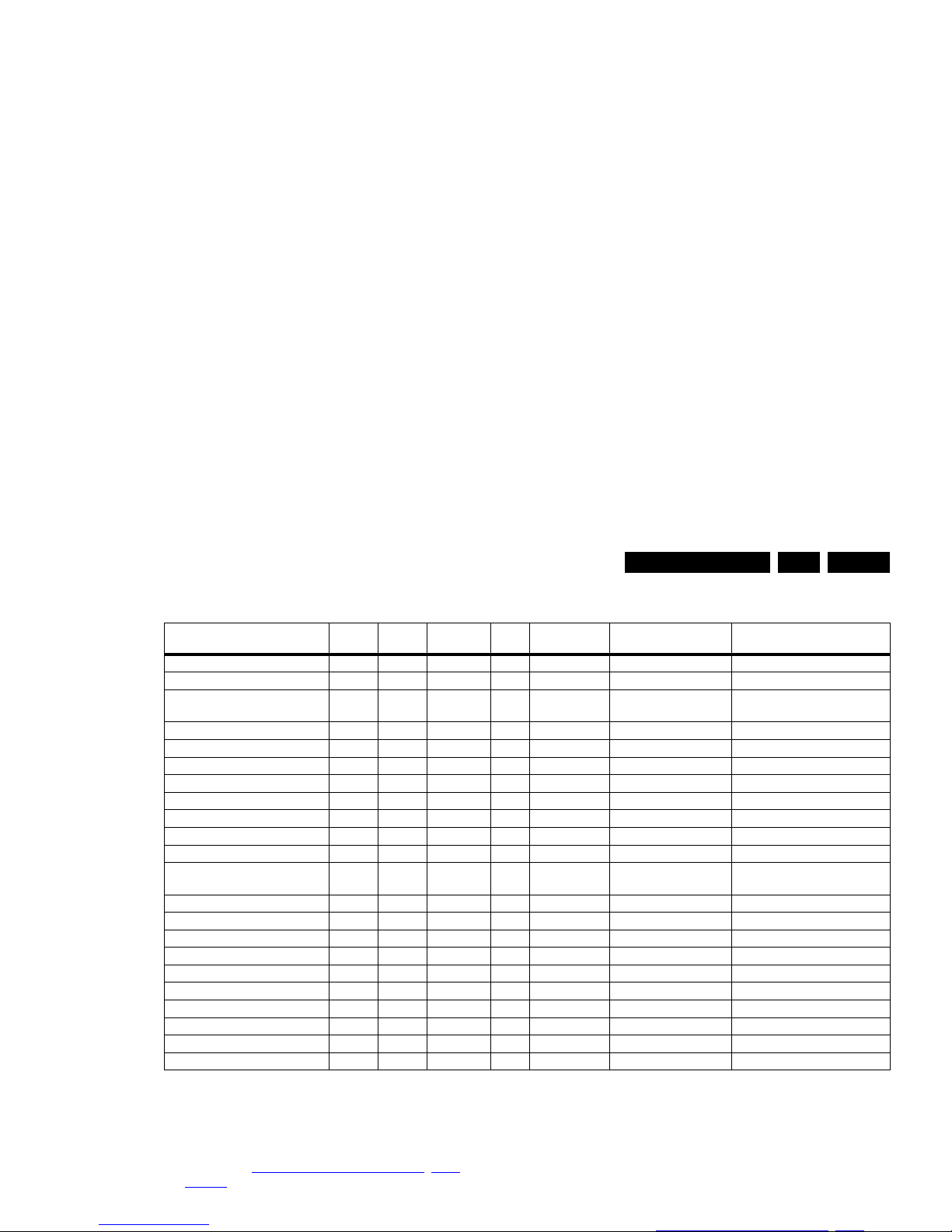
Table 5-2 Error code overview
Extra Info
• Rebooting. When a TV is constantly rebooting due to
internal problems, most of the time no errors will be logged
or blinked. This rebooting can be recognized via a ComPair
interface and Hyperterminal (for Hyperterminal settings,
see section “5.8 Fault Finding and Repair Tips
, 5.8.6
Logging). It’s shown that the loggings which are generated
by the main software keep continuing. In this case
diagnose has to be done via ComPair.
• Error 13 (I
2
C bus 3 blocked). At the time of release of this
• Error 21 (PNX 5100). When there is no I
2
C communication
towards the PNX5100, the TV set will start rebooting and
display LAYER 1 error = 2. Disconnect the mains cord now
and start up the TV set with the solder path (SDM) short to
ground during start-up to activate the LAYER 2 error
blinking. Error “21” will be logged and displayed via the
blinking LED procedure after a few moments from start-up.
Remark : the rebooting can be recognized via a ComPair
interface and Hyperterminal (for Hyperterminal settings,
see section “5.8 Fault Finding and Repair Tips
, 5.8.6
Description Layer 1 Layer 2
Monitored
by
Error/
Prot
Error Buffer/
Blinking LED Device Defective Board
I
2
C3 2 13 MIPS E BL / EB SSB SSB
I
2
C2 2 14 MIPS E BL / EB SSB/Display SSB/display
PNX doesn’t boot (HW cause)
PNX 5100 doesn’t boot
2 15 Stby µP P BL PNX8543/PNX51XX
I
2
C blocked
SSB
12V 3 16 Stby µP P BL / Supply
Inverter or display supply 3 17 MIPS E EB /
1V2, 3V3, 5V to low 2 18 Stby µP P BL / SSB
Temp protection 3 12 MIPS E EB / Display
PNX 5100 2 21 MIPS E EB PNX5100 SSB
HDMI mux 2 23 MIPS E EB TDA9996 SSB
I
2
C switch 2 24 MIPS E EB PCA9540 SSB
Boot-NVM PNX5100 2 25 MIPS E EB STM24C08 SSB
Multi Standard demodulator
(Micronas IF)
2 27 MIPS E EB DRX3616K
DRX3626K
SSB
ARM (ambilight) 8 28 MIPS E EB NXP LPC2103 AL module or DC/DC
FPGA (Local contrast) 2 29 MIPS E EB Altera SSB
Tuner 2 34 MIPS E EB UV1783S/HD1816 SSB
Fan I2C expander 7 41 MIPS E EB PCA9533 FAN module
T° sensor 7 42 MIPS E EB LM 75 T° sensor
FAN 1 7 43 MIPS E EB FAN
FAN 2 7 44 MIPS E EB FAN
Main NVM 2 / MIPS E X STM24C128 SSB
PNX doesn’t boot (SW cause) 2 53 Stby µP E BL PNX8543 SSB
Display (only 56PFL9954H) 5 64 MIPS E BL / EB Altera Display

Service Modes, Error Codes, and Fault Finding
EN 30 Q549.2E LA5.
logged and displayed via the blinking LED procedure when
SDM is switched on.
• Error 42 (Temp sensor). Only applicable for TV sets with
an I
2
C controlled screen.
• Main NVM. When there is no I
2
C communication towards
the main NVM, LAYER 1 error = 2 will be displayed via the
blinking LED procedure. In SDM, LAYER 2 error will be
blinked as “15”. Errors here can not be logged due to
inaccessibility of the NVM device.
• Error 53. This error will indicate that the PNX8543 has
read his bootscript (when this would have failed, error 15
would blink) but initialization was never completed because
of hardware problems (NAND flash, ...) or software
initialization problems. Possible cause could be that there
is no valid software loaded (try to upgrade to the latest main
software version). Note that it can take a few minutes
before the TV starts blinking LAYER 1 error = 2 or in SDM,
LAYER 2 error = 53.
• Error 64. Only applicable for TV sets with an I
2
C controlled
screen .
5.6 The Blinking LED Procedure
5.6.1 Introduction
The blinking LED procedure can be split up into two situations:
• Blinking LED procedure LAYER 1 error. In this case the
error is automatically blinked when the TV is put in CSM.
This will be only one digit error, namely the one that is
referring to the defective board (see table “5-2 Error code
overview”) which causes the failure of the TV. This
approach will especially be used for home repair and call
centres. The aim here is to have service diagnosis from a
distance.
• Blinking LED procedure LAYER 2 error. Via this procedure,
the contents of the error buffer can be made visible via the
front LED. In this case the error contains 2 digits (see table
“5-2 Error code overview
”) and will be displayed when SDM
(hardware pins) is activated. This is especially useful for
fault finding and gives more details regarding the failure of
the defective board.
• Activate the CSM. The blinking front LED will show only
the latest layer 1 error, this works in “normal operation”
mode or automatically when the error/protection is
monitored by the standby processor.
In case no picture is shown and there is no LED blinking,
read the logging to detect whether “error devices” are
mentioned. (see section “5.8 Fault Finding and Repair
Tips, 5.8.6 Logging”).
• Activate the SDM. The blinking front LED will show the
entire content of the LAYER 2 error buffer, this works in
“normal operation” mode or when SDM (via hardware pins)
is activated when the tv set is in protection.
Important remark:
For all errors detected by MIPS which are fatal =>
rebooting of the TV set (reboot starts after LAYER 1 error
blinking), one should short the solder paths at start-up from
the power OFF state by mains interruption and not via the
power button to trigger the SDM via the hardware pins.
• Transmit the commands “MUTE” - “062500” - “OK”
with a normal RC. The complete error buffer is shown.
Take notice that it takes some seconds before the blinking
LED starts.
• Transmit the commands “MUTE” - “06250x” - “OK”
with a normal RC (where “x” is a number between 1
and 5). When x = 1 the last detected error is shown, x = 2
the second last error, etc.... Take notice that it takes some
seconds before the blinking LED starts.
5.7 Protections
5.7.1 Software Protections
Most of the protections and errors use either the stand-by
microprocessor or the MIPS controller as detection device.
Since in these cases, checking of observers, polling of ADCs,
and filtering of input values are all heavily software based,
these protections are referred to as software protections.
There are several types of software related protections, solving
a variety of fault conditions:
• Protections related to supplies: check of the 12V, +5V,
+3V3 and 1V2.
• Protections related to breakdown of the safety check
 Loading...