

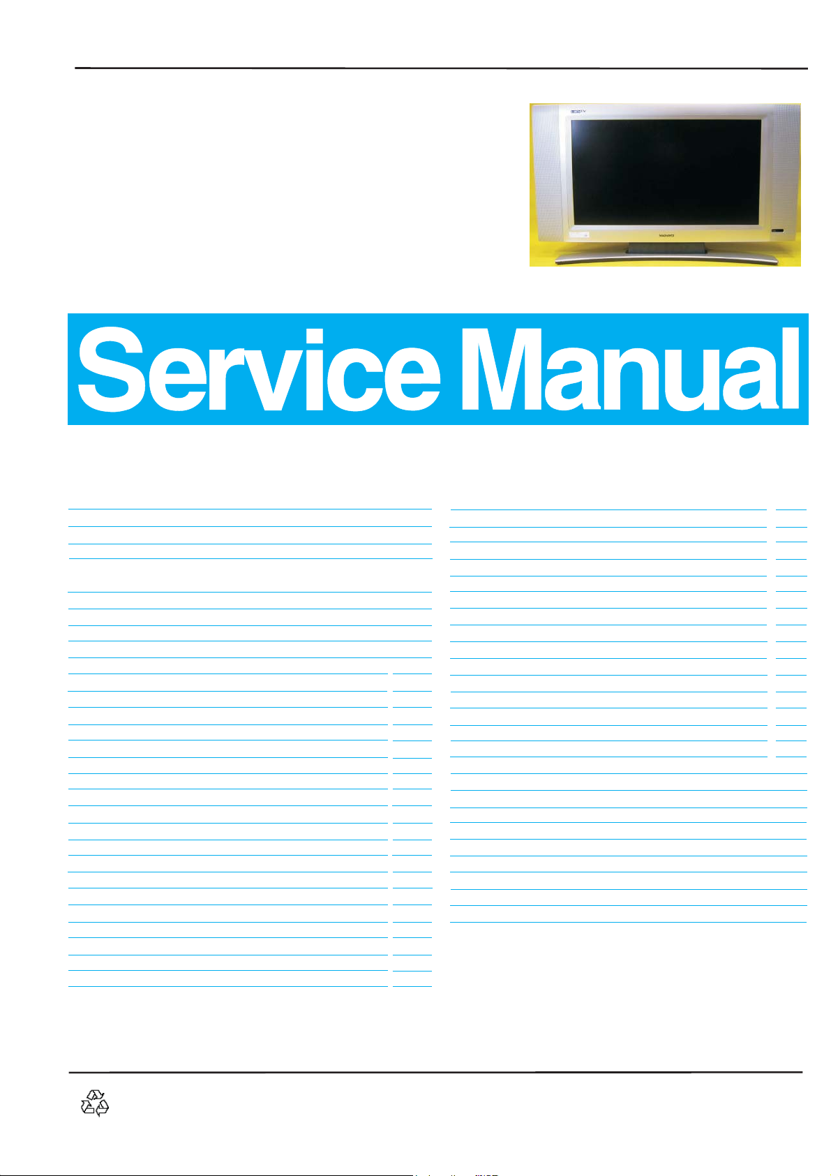
TFT WXGA LCD TV
It`s Free
Service
Service
Service
Service
Service
Service
Chassis: TPE1.0U LA
26MF231D/37
32MF231D/37
37MF231D/37
37MF331D/37
Contents Page
1. Technical Specifications and Connections 2~3
2. Safety Instructions, Warnings and Notes 4
3. Directions for User 6
4. Mechanical Instructions 7~8
5. Service Modes, Error
Codes and Fault Finding 9~15
6. Wiring Diagram 16
Block Diagram 17~20
7. Circuits Diagrams & PWB Layouts
Chassis Overview & Exploded View 21~22
Diagram PWB
Block Diagram
MPIF MAIN: VIDEO SOURCE SELECTION
MPIF MAIN: SUPPLY
MPIF MAIN: IF+SAW FILTER
MPIF MAIN: AUDIO SOURCE SELECTION
MPIF MAIN: AUDIO AMPLIFIER
CHANNEL DECODER
MAIN TUNER
HDMI+SUPPLY
I/O+CONTROL
VIPER: CONTROL
VIPER: MAIN MEMORY
VIPER: A/V+TUNNELBUS
VIPER: SUPPLY
VIPER: EEPROM
MISCELLANEOUS
PNX2015: Audio/Video
PNX2015: DV I/O Interface
PNX2015: Tunnelbus
(Diagram S-A01)23 53~54
(Diagram S-A02)24 53~54
(Diagram S-A03)25 53~54
(Diagram S-A04)26 53~54
(Diagram S-A05)27 53~54
(Diagram S-A06)28 53~54
(Diagram S-A07)29 53~54
(Diagram S-A08)30 53~54
(Diagram S-A09) 31 53~54
(Diagram S-A10)32 53~54
(Diagram S-B11)33 53~54
(Diagram S-B12)34 53~54
(Diagram S-B13)35 53~54
(Diagram S-B14)36 53~54
(Diagram S-B15)37 53~54
(Diagram S-B16)38 53~54
(Diagram S-B17)39 53~54
(Diagram S-B18)40 53~54
(Diagram S-B19)41 53~54
~5
Contents Page
PNX2015: DDR Interface
PNX2015: Standby&Control
PNX2015: Supply
VIPER/PNX2015: Display Interface
VIDEO-DAC
DC/DC (Diagram S-D25)47 53~54
SUPPLY+RS232
AUDIO: AMPLIFIER
AUDIO: CONNECTORS
ANALOG I/O
UART (Diagram S-F30)52 53~54
Power Board (Diagram P)55 56~57
SIDE AV Board (Diagram A)58 59~60
USB Board (Diagram U)61 62~63
IR Board (Diagram I)64 65~66
KEY Board (Diagram K)67 68~69
8. Alignments
Electrical Instructions&Serial NO.Definition 70~73
S
oftware Updrade With Portable Memory 74~75
Trouble Shooting 76
9.
Circuit Description 77~78
IC Data Sheets 79~89
Repair Flow Chart 90~91
10.Spare Parts List 92~97
11.Different Parts List 98~101
12.Revision List 102
(Diagram S-B20)42 53~54
(Diagram S-B21)43 53~54
(Diagram S-B22)44 53~54
(Diagram S-B23)45 53~54
(Diagram S-C24)46 53~54
(Diagram S-D26)48 53~54
(Diagram S-E27)49 53~54
(Diagram S-E28)50 53~54
(Diagram S-F29)51 53~54
Subject to modification Feb. 09 , 2006 EN: 3138 106 50021
PHILIPS

2
It`s Free
TPE1.0U LA
1. Technical Specifications and Connections
1. Technical Specifications and Connections
Index of this chapter:
1.1 Technical Specifications
1.2 Connections
Notes:
·
Some models in this chassis range have a different
mechanical construction. The information given here is
therefore model specific. At the moment of writing, not all
information was available (only the 26-inch TPEB.1U LA
model was available). As soon as the other models are
introduced, an update manual will be released.
·
Figures below can deviate slightly from the actual situation,
due to the different set executions.
·
Specifications are indicative (subject to change).
1.1 Technical Specifications
1.1.1Technical Specifications
1. Vision
Panel Model QD26HL02-01
Display type : LCD
Screen size : 26(66cm), 16:9
Resolution (HxV pixels) : 1366 X 768 (WXGA),
Contrast ratio : 600:1
Light output (cd/m2) : >400
Response time (ms) : 25msec.(Typ.)
Viewing angle (HxV degrees): 170/170 (L/R,U/D) (CR > 10)
Tuning system : PLL
TV Color systems : ATSC,NTSC
Video playback : NTSC
Cable : TD1336/FHGP, ATSC/CLEAR QAM
Tuner bands : Low,Mid,High
Supported video formats : 640 x 480 @60p
2. Sound
Sound systems : Stereo / Virtual Dolby Surround
Maximum power :2x5W(26")
3. Miscellaneous
Power supply:
AC-input : 90V ~ 264VAC,
Normal Operation Power consumption:<110W
Standby power : < 1W (110V/60Hz only)
Power cord length : 1.8M
Power cord type : 3 lead with earth plug ,
Power indicator : LED (On: Green ,
Operating:
Temperature : 0 C to 40 C
Humidity : 10 to 95%(non condensing)
Altitude : 0 to 1,4000 feet
Air pressure : 600 to 4000 mBAR
Note: recommend at 0 to 35 C, Humidity less than 60 %
:
(26")
CLAA320WA01-C(32")
(26")
32(82cm), 16:9 (32")
RGB strip arrangement
(26")
00:1
10 (32")
(26")
500
(32")
(26")
10msec.(Typ.)
(32")
720 x 240 @60p
720 x 480 @60i
720 x 480 @60p
800 x 600 @60p
1280 x 720 @60p
1024 x 768 @60p
1920 x 1080 @60i
2 x 10W(32")
50/60 2Hz
< 140W
plugable(US type)
Standby: No light )
O
O
_
+
(26")
(32")
O
Storage
Temperature : -20 to 60 C
O
Humidity : 10 to 95% (non condensing )
Altitude : 0 to 40000 feet ( non operating )
Air pressure : 600 to 1100 mBAR ( non operating)
Shipping
Temperature : -20 to 60 C
O
Humidity : 10 to 95% (non condensing )
Altitude : 0 to 40000 feet ( non operating )
Air pressure : 600 to 1100 ( non operating )
1.2 Connections
1.2.1Signal Connector
1. Tuner: NAFTA.
2. HDMI IN: HDMI input (TV digital interface support HDCP) with
digital audio or with audio R/L(RCA jack ).
3. AV IN3: Video3 (CVBS, RCA jack) and S-Video share with
same audio R/L (RCA jack ).
4. AV IN1: Video1 (CVBS, RCA jack) and YPbPr component
video1 (RCA jack) share with same audio R/L (RCA jack).
5. AV IN2: Video2 (CVBS, RCA jack) and YPbPr component
video2 (RCA jack) share with same audio R/L (RCA jack).
6. Side AV IN: Side Video (CVBS, RCA jack) and Side S-Video
share with same audio R/L(RCA jack).
7. Headphone OUT : Audio R/L out (mini-jack)
8. SPDIF OUT : (RCA jack)
AV2
S-VHS
AV3
L S/PDIF Pr Pb Y Pr Pb Y
USB
Right CVBS Left Right CVBS Left Right CVBS
Fig1-1
Side AV
S-VHS Right Left CVBS
L eft
Fig1-2
1.2.2 Input signal
1.2.2.1 Signal type
1.2.2.1.1TV Signal type:
RF Signal : Aerial input / 10mV(80dBuV)
Video signal : Video( RCA CVBS input) / 1Vpp (300mV-sync,
700mV-video.) .S video input / 1VppY-signal, 300mVpp
C-signal. COMP Video (Ypbpr input)/ 1Vpp Y signal,
350mVpp Pb,Pr signal
HDMI : Digital interface with 4 channels TMDS signal
Audio signal : Audio (1) R/L for AV IN1 (Video1, Comp video 1
and HDMI ).
Level: - Nominal : 0.5 V rms.
- Maximum : 1.5 V rms.
- Impedance > 10 k .
Audio (2) R/L for AV IN2 (Video2 and Comp-video2).
Level: - Nominal : 0.5 V rms.
- Maximum : 1.5 V rms.
- Impedance > 10 k .
Audio (3) R/L for AV IN3 (Video3 and S-video).
Level: - Nominal : 0.5 V rms.
- Maximum : 1.5 V rms.
- Impedance > 10 k .
Side Audio R/L for Side AV IN3 (Side Video and S-video).
Level: - Nominal : 0.5 V rms.
- Maximum : 1.5 V rms.
- Impedance > 10 k .
AV1
Tuner
HDMI
Headph
1. Technical Specifications and Connections
It`s Free
TPE1.0U LA
3
1.2.2.1.2 Headphone output :
1.2.2 Allowed signal mode specified
1.2.2.1 TV system signal mode:
1.2.3 Signal cable
Audio: R/L output 10mW at 32 .
3.5mm stereo jack with switch
Impedance is between 8 and 600 .
RF support: NAFTA: NTSC(M,N) and ATSC (8VSB and QAM)
Video1,2,3 / S-video1,2: Support, NTSC colour system.
Comp Video (YpbPr): Support NTSC colour system SDTV
and HDTV, including 480i/p, 720p 60Hz, 1080i 60Hz .
HDMI IN : 480i, 480p, 720p/60Hz, 1080i/60Hz
HDMI Pin assignment (Nafta only)
PIN
No.
1 TMDS Data2+
2 TMDS Data2 shield
3 TDMS Data24 TMDS Data1+
5 TMDS Data1 shield
6 TMDS Data17 TMDS Data0+
8 TMDS Data0 shield
9 TMDS Data010 TMDS Clock+
11 TMDS Clock Shield
12 TMDS Clock13 CEC
14 Reserved (N.C. on device)
15 SCL
16 SDA
17 DDC/CEC Ground
18 +5V Power
19 Hot Plug Detect
SIGNAL

4
It`s Free
TPE1.0U LA
2. Safety Instructions, Warnings and Notes
2. Safety Instructions, Warnings and Notes
index of this chapter:
2.1 Safety Instructions
2.2 Warnings
2.3 Notes
2.1 Safety Instructions
Safety regulations require that during a repair:
·
Connect the set to the AC Power via an isolation
transformer (> 800 VA).
·
Replace safety components, indicated by the symbol ,
only by components identical to the original ones. Any
other component substitution (other than original type) may
increase risk of fire or electrical shock hazard.
Safety regulations require that after a repair, the set must be
returned in its original condition. Pay in particular attention to
the following points:
·
Route the wire trees correctly and fix them with the
mounted cable clamps.
·
Check the insulation of the AC Power lead for external
damage.
·
Check the strain relief of the AC Power cord for proper
function.
·
Check the electrical DC resistance between the AC Power
plug and the secondary side (only for sets which have a AC
·
Power isolated power supply):
1. Unplug the AC Power cord and connect a wire
between the two pins of the AC Power plug.
2. Set the AC Power switch to the "on" position (keep the
AC Power cord unplugged!).
3. Measure the resistance value between the pins of the
AC Power plug and the metal shielding of the tuner or
the aerial connection on the set. The reading should be
between 4.5 Mohm and 12 Mohm.
4. Switch "off" the set, and remove the wire between the
two pins of the AC Power plug.
·
Check the cabinet for defects, to avoid touching of any
inner parts by the customer.
2.2 Warnings
·
All ICs and many other semiconductors are susceptible to
electrostatic discharges (ESD ). Careless handling
during repair can reduce life drastically. Make sure that,
during repair, you are connected with the same potential as
the mass of the set by a wristband with resistance. Keep
components and tools also at this same potential.
·
Be careful during measurements in the high voltage
section.
·
Never replace modules or other components while the unit
is switched "on".
·
When you align the set, use plastic rather than metal tools.
This will prevent any short circuits and the danger of a
circuit becoming unstable.
2.3 Notes
2.3.1 General
1. Measure the voltages and waveforms with regard to the
chassis (= tuner) ground ( ), or hot ground ( ), depending
on the tested area of circuitry. The voltages and waveforms
shown in the diagrams are indicative. Measure them in the
Service Default Mode (see chapter 5) with a color bar
signal and stereo sound (L: 3 kHz, R: 1 kHz unless stated
otherwise) and picture carrier at 475.25 MHz for PAL, or
61.25 MHz for NTSC (channel 3).
2. Where necessary, measure the waveforms and voltages
with ( ) and without ( ) aerial signal. Measure the
voltages in the power supply section both in normal
operation ( ) and in stand-by ( ). These values are
indicated by means of the appropriate symbols.
3. The semiconductors indicated in the circuit diagram and in
the parts lists, are interchangeable per position with the
semiconductors in the unit, irrespective of the type
indication on these semiconductors.
4. Manufactured under license from Dolby Laboratories.
"Dolby" and the "double-D symbol", are trademarks of
Dolby Laboratories.
2.3.2 Schematic Notes
1. All resistor values are in ohms and the value multiplier is
often used to indicate the decimal point location (e.g. 2K2
indicates 2.2 kohm).
2. Resistor values with no multiplier may be indicated with
either an "E" or an "R" (e.g. 220E or 220R indicates 220
ohm).
3. All capacitor values are given in micro-farads (u= x10 ),
nano-farads (n= x10 ), or pico-farads (p= x10 ).
4. Capacitor values may also use the value multiplier as the
decimal point indication (e.g. 2p2 indicates 2.2 pF).
5. An "asterisk" (*) indicates component usage varies. Refer
to the diversity tables for the correct values.
6. The correct component values are listed in the Electrical
Replacement Parts List. Therefore, always check this list
when there is any doubt.
-9
-12
-6
2.3.3 Rework on BGA (Ball Grid Array) Ics
General
Although (LF)BGA assembly yields are very high, there may still be
a requirement for component rework. By rework, we mean the
process of removing the component from the PWB and replacing it
with a new component. If an (LF)BGA is removed from a PWB, the
solder balls of the component are deformed drastically so the
removed (LF)BGA has to be discarded.
Device Removal
As is the case with any component that, it is essential when
removing an (LF)BGA, the board, tracks, solder lands, or
surrounding components are not damaged. To remove an(LF)BGA,
the board must be uniformly heated to a temperature close to the
reflow soldering temperature. A uniform temperature reduces the
chance of warping the PWB.To do this, we recommend that the
board is heated until it is certain that all the joints are molten.
Then carefully pull the component off the board with a vacuum
nozzle. For the appropriate temperature profiles, see the IC data
sheet.
Area Preparation
When the component has been removed, the vacant IC area must
be cleaned before replacing the (LF)BGA.Removing an IC often
leaves varying amounts of solder on the mounting lands. This
excessive solder can be removed with either a solder sucker or
solder wick. The remaining flux can be removed with a brush and
cleaning agent.After the board is properly cleaned and inspected,
apply flux on the solder lands and on the connection balls of
the (LF)BGA.
Note: Do not apply solder paste, as this has shown to result in
problems during re-soldering.
Device Replacement
The last step in the repair process is to solder the new component
on the board. Ideally, the (LF)BGAshould be aligned under a
microscope or magnifying glass. If this is not possible, try to align
the (LF)BGA with any board markers. To reflow the solder, apply a
temperature profile according to the IC data sheet. So as not to
damage neighbouring components, it may be necessary to reduce
some temperatures and times.
More Information
For more information on how to handle BGA devices, visit this
URL: (needs subscription,
www.atyourservice.ce.philips.com
not available for all regions). After login, "select Magazine", then
go to "Workshop Information". Here you will find Information on
how to deal with BGA-ICs.

2. Safety Instructions, Warnings and Notes
It`s Free
TPE1.0U LA
5
2.3.4 Lead Free Solder
Philips CE is going to produce lead-free sets (PBF) from
1.1.2005 onwards.
Lead-free sets will be indicated by the PHILIPS-lead-free logo
on the Printed Wiring Boards (PWB):
Fig 2-1 Lead-free logo
This sign normally has a diameter of 6 mm, but if there is less
space on a board also 3 mm is possible.
In case of doubt wether the board is lead-free or not (or with
mixed technologies), you can use the following method:
1. Always use the highest temperature to solder, when using
SAC305 (see also instructions below).
2. De-solder thoroughly (clean solder joints to avoid mix of
two alloys).
Caution
which is coupled to the 12NC. For an overview of these
profiles, visit the website
(needs subscription, but is not available for all regions)
You will find this and more technical information within the
"Magazine", chapter "Workshop information".
For additional questions please contact your local repairhelpdesk.
: For BGA-ICs, you must use the correct temperatureprofile,
www.atyourservice.ce.philips.com
In case of doubt whether the board is lead-free or not (or with
mixed technologies), you can use the following method:
·
Always use the highest temperature to solder, when using
SAC305 (see also instructions below).
·
De-solder thoroughly (clean solder joints to avoid mix of
two alloys).
Caution must
which is coupled to the 12NC. For an overview of these
profiles, visit the website
(needs subscription, but is not available for all regions)
You will find this and more technical information within the
"Magazine", chapter "Workshop information".
For additional questions please contact your local repair help
desk.
: For BGA-ICs, you use the correct temperatureprofile,
www.atyourservice.ce.philips.com
2.3.5 Practical Service Precautions
It makes sense to avoid exposure to electrical shock.
1.
While some sources are expected to have a possible
dangerous impact, others of quite high potential are of
limited current and are sometimes held in less regard.
Always respect voltages.
2. While some may not be
dangerous in themselves, they can cause unexpected
reactions - reactions that are best avoided. Before reaching
into a powered TV set, it is best to test the high voltage
insulation. It is easy to do, and is a good service precaution.
Due to lead-free technology some rules have to be respected
by the workshop during a repair:
1. Use only lead-free soldering tin . If lead-free solder paste
is required,please contact the manufacturer of your soldering
equipment. In general, use of solder paste within
workshops should be avoided because paste is not easy to
store and to handle.
2. Use only adequate solder tools applicable for lead-free
soldering tin. The solder tool must be able
-To reach at least a solder-tip temperature of 400 C.
-To stabilise the adjusted temperature at the solder-tip.
-To exchange solder-tips for different applications.
3. Adjust your solder tool so that a temperature around 360 C
- 380 C is reached and stabilised at the solder joint.
Heating time of the solder-joint should not exceed~4sec.
Avoid temperatures above 400 C, otherwise wear-out of
tips will rise drastically and flux-fluid will be destroyed. To
avoid wear-out of tips, switch "off" unused equipment or
reduce heat.
4. Mix of lead-free soldering tin/parts with leaded soldering
tin/parts is possible but PHILIPS recommends strongly to
avoid mixed regimes. If not to avoid, clean carefully the
solder-joint from old tin and re-solder with new tin.
5. Use only original spare-parts listed in the Service-Manuals.
Not listed standard material (commodities) has to be
purchased at external companies.
6. Special information for lead-free BGA ICs: these ICs will be
delivered in so-called "dry-packaging" to protect the IC
against moisture. This packaging may only be opened
short before it is used (soldered). Otherwise the body of the
IC gets "wet" inside and during the heating time the
structure of the IC will be destroyed due to high (steam-)
pressure inside the body. If the packaging was opened
before usage, the IC has to be heated up for some hours
(around 90C)fordrying (think of ESD-protection !).
Do not re-use BGAs at all!
7. For sets produced before 1.1.2005, containing leaded
soldering tin and components, all needed spare parts will
be available till the end of the service period. For the repair
of such sets nothing changes.

6
It`s Free
TPE1.0U LA
3. Directions for Use
3. Directions for Use
You can download this information from the following websites:
http://www.philips.com/support
http://www.p4c.philips.com

4. Mechanical Instructions
It`s Free
Index of this chapter:
4.1 Assy/Panel Removal
4.2 Set Re-assembly
4.1 Assy/Panel Removal
Front view
Back view
4. Mechanical Instructions
Fig.1
Fig.6
TPE1.0U LA
Fig.8
7
Fig.7
Fig.2
Step 1. Remove the stand.
Remove the three screws as Fig.3 and Fig.4
Fig.3
Step 2. Remove the Back cover and Main shield assy as Fig.5~12.
a.
Remove the 7 screws on the sides as Fig.5and the other 2 screws
b. Use thin "I" type screwdriver to open 4 clicks on bottom
side as Fig.6
c.
Use thin "I" type screwdriver to open 2 clicks on right
side as Fig.7
e. Use thin "I" type screwdriver to open 2 clicks on left
side as Fig.8
f. Use thin "I" type screwdriver to open 6 clicks on top
side as Fig.9
g. Remove the back cover as Fig.10 .
h. Remove the 13 screws as Fig.10,Fig.11,Fig.12 , then remove the
Main shield assy.
Fig.4
Fig.9
Fig. 10
Fig. 11
Fig. 12
Step 3. Remove the Scaler, Power,IR, Key Control, Side AV and USB
board.
Remove the 14 screws and disconnect the 12 cables as Fig. 13 .
Fig.5
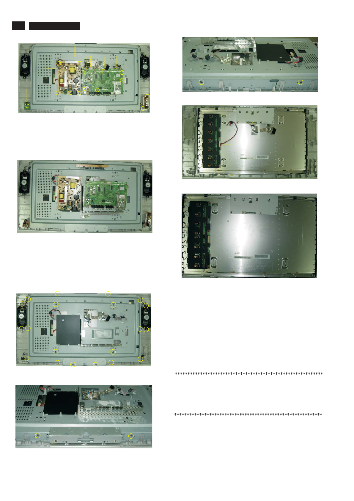
8
It`s Free
Step 4. Disconnect the USB PCB, the Side AV PCB, the KEY PCB , the
TPE1.0U LA
Fig. 13
IR PCB, as Fig.14 .the Scaler PCB and power PCB
4. Mechanical Instructions
Fig. 17
Fig. 18
Fig. 14
Step 5 Remove the MAIN Frame ASSY as Fig.15~Fig.17
a.
Remove the 24 screws as Fig.15~17 .
Step 6 Remove the Bezel assy as Fig.18~Fig.19 .
a. as Fig.18 .
Remove the 2 connectors
b . as Fig.19 .
Remove the Bezel assy
Fig. 15
Fig. 19
4.2 Set Re-assembly
To re-assemble the whole set, execute all processes in reverse
order.
Notes:
a. While re-assembling, make sure that all cables are placed
and connected in their original position.
b. Pay special attention not to damage the EMC foams at the
SSB shielding. Check that EMC foams are put correctly on
their places.
In warranty, it is not allowed to disassembly the LCD panel, even the
backlight unit defect.
Out of warranty, the replacment of backlight unit is a correct way
when the defect is cused by backlight (CCFL,Lamp).
Fig. 16

5. Service Modes, Error Codes and Fault Finding
It`s Free
5. Service Modes, Error Codes and Fault Finding
index of this chapter:
5.1 Test Points
5.2 Service Modes
5.3 Stepwise Start-up
5.4 ComPair
5.5 Error Codes
5.6 The Blinking LED Procedure
5.7 Protections
5.1 Test Points
The chassis is equipped with test points (Fxxx) printed on the
circuit board assemblies. As most signals are digital, it will be
almost impossible to measure waveforms with a standard
oscilloscope. Therefore, waveforms are not given in this
manual. Several key ICs are capable of generating test
patterns, which can be controlled via ComPair. In this way it is
possible to determine which part is defective.
Perform measurements under the following conditions:
·
Service Default Mode.
·
Video: Color bar signal.
·
Audio: 3 kHz left, 1 kHz right.
5.2 Service Modes
Service Default Mode (SDM) and Service Alignment Mode
(SAM) offer several features for the service technician, while
the Customer Service Mode (CSM) is used for communication
between a Customer Helpdesk and a customer.
There is also the option of using ComPair, a hardware interface
between a computer (see requirements below) and the TV
chassis. It offers the ability of structured troubleshooting, test
pattern generation, error code reading, software version
readout, and software upgrading.
Minimum
Windows 95/98, and a CD-ROM drive (see also paragraph "
ComPair").
requirements for ComPair: a Pentium processor,
5.2.1 Service Default Mode (SDM)
Purpose
·
To create a pre-defined setting, to get the same
measurement results as given in this manual.
·
To override SW protections (only applicable for protections
detected by stand-by processor) and make the TV start up
to the step just before protection (a sort of automatic
stepwise start up). See paragraph Stepwise Start Up .
·
To start the blinking LED procedure (not valid in protection
mode).
Specifications
·
Tuning frequency 61.25 MHz for NTSC: The TV shall tune
to physical channel 3 only if channel 3 is an analog channel
or if there is no channel 3 installed in the channel map. If
there is a digital channel installed in channel 3, then the
frequency to which the set will tune, would be as specified
in the channel map and could be different from the one
corresponding to the physical channel 3.
·
All picture settings at 50% (brightness, color, contrast).
All sound settings at 50%, except volume at 25%.
·
·
All service-unfriendly modes (if present) are disabled, like:
- (Sleep) timer.
- Child/parental lock.
- Picture mute (blue mute or black mute).
- Automatic volume levelling (AVL).
- Auto switch "off" (when no video signal was received
for 10 minutes).
- Skip/blank of non-favorite pre-sets.
"
"
How to Activate SDM
Use one of the following methods:
·
·
After activating this mode, will appear in the upper right
corner of the screen (if you have picture).
How to Navigate
When you press the button on the RC transmitter, the
set will toggle between the SDM and the normal user menu
(with the SDM mode still active in the background).
How to Exit SDM
Use one of the following methods:
·
·
5.2.2 Service Alignment Mode (SAM)
Purpose
·
·
·
·
·
How to Activate SAM
Via a standard RC transmitter: key in the code
directly followed by the button. After activating SAM
with this method a service warning will appear on the screen,
you can continue by pressing the red button on the RC.
Contents of SAM:
·
·
·
·
TPE1.0U LA
-
Smart modes.
-
Auto store of personal presets.
-
Auto user menu time-out.
Use the standard RC-transmitter and key in the code
directly followed by the "MENU"
: It is possible that, together with the SDM, the main
Note
menu will appear. To switch it "off", push the button again.
Short for a moment the two solder pads [1] on the SSB,
with the indication
shielding. Activation can be performed in all modes, except
when the set has a problem with the Stand-by Processor.
Switch the set to STAND-BY via the RC-transmitter.
Via a standard customer RC-transmitter: key in
sequence.
To perform (software) alignments.
To change option settings.
To easily identify the used software version.
To view operation hours.
To display (or clear) the error code buffer.
Hardware Info.
- Displays the software version
A. VIPER SW Version.
of the VIPER software (main software) (example:
BX23U-1.2.3.4_12345 = AAAAB_X.Y.W.Z_NNNNN).
·
·
·
·
- Displays the software version
B. SBY PROC Version.
of the stand-by processor.
- Displays the production code of
C. Production Code.
the TV, this is the serial number as printed on the back
of the TV set. Note that if an NVM is replaced or is
initialized after corruption, this production code has to
be re-written to NVM. ComPair will foresee in a
possibility to do this.
Operation Hours.
operation hours (not the stand-by hours). Every time the
TV is switched "on/off", 0.5 hours is added to this number.
Errors.
error is displayed at the upper left (for an error explanation
see paragraph "Error Codes").
Defective Module.
= the chassis name.
AAAA
= the region: A= AP, E= EU, L= Latam,U=US.
B
X.Y.W.Z
main version number (different numbers are not
compatible with one another) and Y is the sub
version number (a higher number is always
compatible with a lower number). The last two
digits are used for development reasons only, so
they will always be zero in official releases.
NNNNN
software.
(Followed by maximal 10 errors). The most recent
"SDM". They are located outside the
"MENU"
"INFO"
= the software version, where X is the
= last five digits of 12nc code of the
Displays the accumulated total of
Here the module that generates the
button.
"MENU"
"SDM"
"062596" ,
"00"-
"062596"
9

10
It`s Free
TPE1.0U LA
5. Service Modes, Error Codes and Fault Finding
error is displayed. If there are multiple errors in the buffer, which are
not all generated by a single module, there is probably another
defect. It will then display the message here.
·
Reset Error Buffer.
then the button, the error buffer is reset.
·
Alignments.
·
Dealer Options.
·
Options.
·
Initialize NVM.
in the former EMG based chassis, the microprocessor
replaces the content with default data (to assure that the
set can operate). However, all preferences and alignment
values are gone now, and option numbers are not correct.
Therefore, this was a very drastic way. In this chassis, the
procedure is implemented in another way: The moment the
processor recognizes a corrupted NVM, the initialize NVM line will
be highlighted. Now, you can do two things(dependent of the service
instructions at that moment):
- Save the content of the NVM via ComPair for
- Initialize the NVM (same as in the past, however now it
Note
the NVM, there is a high possibility that you will not have picture
any more because your display option is not correct. So, before
you can initialize your NVM via the SAM, you need to have a
picture and therefore you need the correct display option. To
adapt this option, use ComPair. The correct HEX values for the
options can be found in the table below.
·
Store
pressing and then the
·
SW Maintenance.
- Not useful for service purposes. In case of
- . Not functional at the moment this manual
How to Navigate
·
In SAM, you can select the menu items with the
UP/DOWN"
will be highlighted. When not all menu items fit on the
screen, move the key to display the
next/previous menu items.
·
With the keys, it is possible to:
- (De) activate the selected menu item.
- (De) activate the selected submenu.
How to Exit SAM
Use one of the following methods:
·
Press the button on the RC-transmitter.
·
Switch the set to STAND-BY via the RC-transmitter.
Note
a channel. This could hamper the White Point alignments
because you cannot choose your channel/frequency any more.
Workaround: after you have sent the RC code ,you
will see the service-warning screen, and in this stage it is still possible
to change the channel (so before pressing the button).
"OK"
Extra features for Service.
development analysis, before initializing. This will give
the Service department an extra possibility for
diagnosis (e.g. when Development asks for this).
happens conscious).
: When you have a corrupted NVM, or you have replaced
. All options and alignments are stored when
"cursor right" "OK" button.
SW Events.
specific software problems, the development
department can ask for this info.
HW Events
is released, description will be published in an update
manual if the function becomes available.
key on the RC-transmitter. The selected item
"CURSOR LEFT/RIGHT"
"MENU"
: As long as SAM is activated, it is not possible to change
When you press and
This will activate the submenu.
Extra features for the dealers.
When an NVM was corrupted (or replaced)
"CURSOR UP/DOWN"
"UNKNOWN"
"cursor right"
"ALIGNMENTS"
""
"CURSOR
"062596 INFO"
"OK"
5.2.3 Customer Service Mode (CSM)
Purpose
When a customer is having problems with his TV-set, he can
call his dealer or the Customer Helpdesk. The service
technician can then ask the customer to activate the CSM, in
order to identify the status of the set. Now, the service
technician can judge the severity of the complaint. In many
cases, he can advise the customer how to solve the problem,
or he can decide if it is necessary to visit the customer.
The CSM is a read only mode; therefore, modifications in this
mode are not possible.
How to Activate CSM
Key in the code via the standard RC transmitter.
: Activation of the CSM is only possible if there is no (user)
Note
menu on the screen!
How to Navigate
By means of the knob on the RCtransmitter,
you can navigate through the menus.
Contents of CSM
·
SW Version
the built-in main software version. In case of field problems
related to software, software can be upgraded. As this
software is consumer upgradeable, it will also be published
on the Internet.
·
SBY Processor Version
processor software version. Upgrading this software will be
possible via a PC and a ComPair interface (see chapter
Software upgrade).
·
Set Type
workshop as reference for further diagnosis. In this way, it
is not necessary for the customer to look at the rear of the
TV-set. Note that if an NVM is replaced or is initialized after
corruption, this set type has to be re-written to NVM.
ComPair will foresee a possibility to do this.
·
Production Code
number) of the TV. Note that if an NVM is replaced or is
initialized after corruption, this production code has to be
re-written to NVM. ComPair will foresee a possibility to do this.
·
Code 1
soon as the built-in diagnose software has detected an
error the buffer is adapted. The last occurred error is
displayed on the leftmost position. Each error code is
displayed as a 2-digit number. When less than 10 errors
occur, the rest of the buffer is empty (00). See also
paragraph Error Codes for a description.
·
Code 2
also paragraph Error Codes for a description.
·
Headphone Volume
headphone volume, as set by the customer. The value can
vary from 0 (volume is minimum) to 100 (volume is
maximum). Change via
"HEADPHONE VOLUME".
·
. Indicates whether the received transmitter
Dolby
transmits Dolby sound (
presence of Dolby can only be tested by the software on
the Dolby Signaling bit. If a Dolby transmission is received
without a Dolby Signaling bit, this indicator will show
even though a Dolby transmission is received.
·
Sound Mode
sound mode (or automatically chosen mode). Possible
values are and VIRTUAL DOLBY
SURROUND
"SOUND MODE". It can also have been selected
automatically by signaling bits (internal software).
·
Tuner Frequency
·
Digital Processing
Possible values are and
Change via
PROCESSING".
·
TV System
the selected transmitter.
- M: NTSC M signal received
- ATSC: ATSC signal received
·
Center Mode
·
DNR
. Gives the selected DNR setting (Dynamic Noise
Reduction), , or
Change via "MENU", "TV","PICTURE","DNR".
·
"123654"
"CURSOR-DOWN/UP"
(example: BX23U-1.2.3.4_12345). Displays
. Displays the built-in stand-by
. This information is very helpful for a helpdesk/
. Displays the production code (the serial
. Gives the latest five errors of the error buffer. As
. Gives the first five errors of the error buffer. See
. Gives the last status of the
"MENU","TV","SOUND",
"ON") or not ("OFF").Attention:The
"OFF"
. Indicates the by the customer selected
"STEREO" "
".Change via "MENU","TV","SOUND",
. Not applicable for US sets.
. Indicates the selected digital mode.
"STANDARD" "PIXEL PLUS".
"MENU","TV","PICTURE","DIGITAL
. Gives information about the video system of
. Not applicable.
"OFF","MINIMUM","MEDIUM" "MAXIMUM".
.Gives the noise ratio for the selectedNoise Figure

5. Service Modes, Error Codes and Fault Finding
It`s Free
TPE1.0U LA
11
transmitter. This value can vary from 0 (good signal) to 127
(average signal) and to 255 (bad signal). For some
software versions, the noise figure will only be valid when
"Active Control" is set to "medium" and "maximum"
before
activating CSM.
·
. Indicates which source is used and the video/
Source
audio signal quality of the selected source. (Example:
Tuner, Video/NICAM) Source:
"TUNER","AV1","AV2",
automatic stepwise start-up. In combination with the start-up
diagrams below, you can see which supplies are present at a
certain moment.
Important to know here is, that if e.g. the 3V3 detection fails
(and thus error 11 is blinking) and the TV is restarted via SDM,
the Stand-by Processor will enable the 3V3, but will not go to
protection now. The TV will stay in this situation until it is reset
(Mains/AC Power supply interrupted).
"AV3","HDMI 1","SIDE". Video signal quality:"VIDEO",
"S-VIDEO","RGB 1FH","YPBPR 1FH 480P","YPBPR 1FH
576P","YPBPR 1FH 1080I","YPBPR 2FH 480P","YPBPR
2FH 576P","YPBPR 2FH 1080I","RGB 2FH 480P","RGB
2FH 576P" or "RGB 2FH 1080I". Audio signal quality:
"STEREO","SPDIF 1","SPDIF 2" or "SPDIF".
·
Audio System
system. Possible values are Stereo , Mono , Mono
selected , Analog In: No Dig. Audio , Dolby Digital 1+1
. Gives information about the audible audio
"""""
"" "" ",
"Dolby Digital 1/0","Dolby Digital 2/0","Dolby Digital 2/1",
"Dolby Digital 2/2","Dolby Digital 3/0","Dolby Digital 3/1",
"Dolby Digital 3/2","Dolby Digital Dual I","Dolby Digital
Dual II","MPEG 1+1","MPEG 1/0","MPEG 2/0". This is the
same info as you will see when pressing the "INFO" button
in normal user mode (item "signal"). In case of ATSC
receiving there will be no info displayed.
·
Tuned Bit
·
Preset Lock
lock: LOCKED or UNLOCKED . Change via
. Not applicable for US sets.
. Indicates if the selected preset has a child
" " " " "MENU",
"TV","CHANNELS","CHANNEL LOCK".
·
Lock After
OFF or e.g. 18:45 (lock time). Change MENU , TV ,
"" " " " """
CHANNELS , LOCK AFTER .
""" "
TV Ratings Lock
the customer. Change via MENU , TV , CHANNELS ,
TV RATING LOCK . Possible values are: ALL , NONE , TV-Y ,
"" """"""
TV-Y7 , TV-G , TV-PG , TV14 and TV-MA .
""""" """" "
·
Movie Ratings Lock
set by the customer. Change via MENU , TV , CHANNELS ,
MOVIE RATINGS LOCK .Possible values are: ALL , NR , G
"""""""",
PG , PG-13,R,NC-17 and X .
""" """" " ""
·
V-Chip Tv Status
. Indicates at what time the channel lock is s
. Indicates the TV ratings lock as set by
""
""""" "
. Indicates the Movie Ratings Lock as
""
""""" "
. Indicates the setting of the V-chip as
applied by the selected TV channel. Same values can be
shown as for TV RATINGS LOCK .
·
V-Chip Movie Status
""
. Indicates the setting of the V-chip
as applied by the selected TV channel. Same values can
be shown as for MOVIE RATINGS LOCK .
·
Options 1
""
. Gives the option codes of option group 1 as set
in SAM (Service Alignment Mode).
·
Options 2
. Gives the option codes of option group 2 as set
in SAM (Service Alignment Mode).
·
AVL
. Indicates the last status of AVL (Automatic Volume
" " " " " " " "," " " "
Level): ON or OFF . Change via: MENU , TV SOUND , AVL .
AVL can not be set in case of digital audio reception (e.g.
Dolby Digital or AC3).
·
Delta Volume
for the selected preset as set by the customer: from -12
" ". " "" "" "" "
to +12 Change via MENU , TV , SOUND , DELTA VOLUME .
·
HDMI key validity
·
IEEE key validity
·
POD key validity
·
Digital Signal Quality
. Indicates the last status of the delta volume
""
. Indicates the key
. Indicates the key
. Indicates the key
's validity.
's validity(n.a.).
's validity.
. Indicates quality of the received
digital signal (0= low).
How to Exit CSM
Press any key on the RC-transmitter (with exception of the
""""""
CHANNEL +/- , VOLUME , MUTE and digit (0-9) keys).
5.3 Stepwise Start-up
The stepwise start-up method, as known from FTL/FTP sets is
not valid any more. The situation for this chassis is as follows:
when the TV is in a protection state detected via the Stand-by
Processor (and thus blinking an error) and SDM is activated via
shortcutting the pins on the SSB, the TV starts up until it
reaches the situation just before protection. So, this is a kind of
Stand-by
(Off St-by)
- POD Cardremove
- Tact SW pushed
5.4 ComPair
5.4.1 Introduction
ComPair (Computer Aided Repair) is a service tool for Philips
Consumer Electronics products. ComPair is a further
development on the European DST (service remote control),
which allows faster and more accurate diagnostics. ComPair
has three big advantages:
·
ComPair helps you to quickly get an understanding on how
to repair the chassis in a short time by guiding you
systematically through the repair procedures.
·
ComPair allows very detailed diagnostics (on I C level) and
is therefore capable of accurately indicating problem areas.
You do not have to know anything aboutICcommands
yourself because ComPair takes care of this.
·
ComPair speeds up the repair time since it can
automatically communicate with the chassis (when the
microprocessor is working) and all repair information is
directly available. When ComPair is installed together with
the Force/SearchMan electronic manual of the defective
chassis, schematics and PWBs are only a mouse click away.
5.4.2 Specifications
ComPair consists of a Windows based fault finding program
and an interface box between PC and the (defective) product.
The ComPair interface box is connected to the PC via a serial
(or RS-232) cable.
For this chassis, the ComPair interface box and the TV
communicate via a bi-directional service cable via the service
connector(s).
·
Automatic (by communication with the television): ComPair
can automatically read out the contents of the entire error
buffer. Diagnosis is done on I C/UART level. ComPair can
Off
- WakeUprequested
- Acquisition needed
Semi
- No dataAcquisition required
and no PODpresent
- Tact SW pushed
- WakeUprequested
- Acquisition needed
POD
Stand-by
No data Acquisition
required and
POD present
GoToProtection
Stand-by
Fig. 5-1 Transition diagram
2
GoToProtection
WakeUp
requested
- St-by requested
- Tact SW pushed
WakeUp
requested
2
2
Active
GoToProtection
Protection

12
It`s Free
access the I C/UART bus of the television. ComPair can
send and receive I C/UART commands to the micro
TPE1.0U LA
2
2
5. Service Modes, Error Codes and Fault Finding
controller of the television. In this way, it is possible for
ComPair to communicate (read and write) to devices on
2
the I C/UART buses of the TV-set.
·
Manually (by asking questions to you): Automatic
diagnosis is only possible if the micro controller of the
television is working correctly and only to a certain extend.
When this is not the case, ComPair will guide you through
the fault finding tree by asking you questions (e.g.
Does the
screen give a picture? Click on the correct answer: YES /
) and showing you examples (e.g.
NO Measure test-point I7
and click on the correct oscillogram you see on the
oscilloscope
). You can answer by clicking on a link (e.g.
text or a waveform picture) that will bring you to the next
step in the fault finding process.
By a combination of automatic diagnostics and an interactive
question / answer procedure, ComPair will enable you to find
most problems in a fast and effective way.
5.4.3 How to Connect
This is described in the chassis fault finding database in
ComPair.
Caution: It is compulsory to connect the TV to the PC as
shown in the picture below (with the ComPair interface in
between), as the ComPair interface acts as a level shifter. If
you connect the TV directly to the PC (via UART), the VIPER
or PNX2015 will be blown!
TO
UART SERVICE
CONNECTOR
TO
2
I C SERVICE
CONNECTOR
When multiple errors occur (errors occurred within a short time
span), there is a high probability that there is some relation
between them.
Basically there are three kinds of errors:
·
Errors detected by the Stand-by Processor
. These
errors will always lead to protection and an automatic start
of the blinking LED for the concerned error (see paragraph
""
The Blinking LED Procedure ). In these cases SDM can
be used to start up (see chapter Stepwise Start-up ).
·
Errors detected by VIPER that lead to protection
""
. In this case
the TV will go to protection and the front LED will blink at 3 Hz.
Further diagnosis via service modes is not possible here (see also
paragraph Error Codes -> Error Buffer -> Extra Info ).
·
Errors detected by VIPER that do not lead to protection
""""""
. In this
case the error can be read out via ComPair, via blinking LED
method, or in case you have picture, via SAM.
5.5.2 How to Read the Error Buffer
Use one of the following methods:
·
On screen via the SAM (only if you have a picture). E.g.:
- 00 00 00 00 00: No errors detected
- 06 00 00 00 00: Error code 6 is the last and only
detected error
- 09 06 00 00 00: Error code 6 was first detected and
error code 9 is the last detected error
·
Via the blinking LED procedure (when you have no
picture). See next paragraph.
·
Via ComPair.
5.5.3 How to Clear the Error Buffer
Use one of the following methods:
·
By activation of the RESET ERROR BUFFER command
""
in the SAM menu.
·
With a normal RC, key in sequence MUTE followed by
""""
062599 and OK .
·
If the content of the error buffer has not changed for 50+
""
hours, it resets automatically.
Fig. 5-2 ComPair interface connection
5.4.4 How to Order
ComPair order codes (US):
·
ComPair Software: ST4191.
·
ComPair Interface Box: 4822 727 21631.
·
AC Adapter: T405-ND.
·
ComPair Quick Start Guide: ST4190.
·
ComPair interface extension cable: 3139 131 03791.
·
ComPair UART interface cable: 3122 785 90630
: If you encounter any problems, contact your local
Note
support desk.
5.5 Error Codes
5.5.1 Introduction
The error code buffer contains all detected errors since the last
time the buffer was erased. The buffer is written from left to
right, new errors are logged at the left side, and all other errors
shift one position to the right.
When an error has occurred, the error is added to the list of
errors, provided the list is not full or the error is a protection
error.
When an error occurs and the error buffer is full, then the new
error is not added, and the error buffer stays intact (history is
maintained), except when the error is a protection error.
To prevent that an occasional error stays in the list forever, the
error is removed from the list after 50+ operation hours.
5.5.4 Error Buffer
In case of non-intermittent faults, clear the error buffer before
you begin the repair (before clearing the buffer, write down the
content, as this history can give you significant information).
This to ensure that old error codes are no longer present.
If possible, check the entire contents of the error buffer. In
some situations, an error code is only the result of another error
code and not the actual cause (e.g., a fault in the protection
detection circuitry can also lead to a protection).
There are several mechanisms of error detection:
Via error bits in the status registers of ICs.
Via polling on I/O pins going to the stand-by processor.
Via sensing of analogue values on the stand-by processor.
""
Via a not acknowledge of an I C communication.
2
Take notice that some errors need more than 90 seconds
before they start blinking. So in case of problems wait 2
minutes from start-up onwards, and then check if the front LED
is blinking.
5.6 The Blinking LED Procedure
5.6.1 Introduction
The blinking LED procedure can be split up into two situations:
·
Blinking LED procedure in case of a protection detected by
the stand-by processor. In this case the error is
automatically blinked. This will be only one error, namely
the one that is causing the protection. Therefore, you do
not have to do anything special, just read out the blinks. A
long blink indicates the decimal digit, a short blink indicates
the units.
·
Blinking LED procedure in the state. Via this
procedure, you can make the contents of the error buffer
"ON"

5. Service Modes, Error Codes and Fault Finding
It`s Free
TPE1.0U LA
13
visible via the front LED. This is especially useful for fault
finding, when there is no picture.
When the blinking LED procedure is activated in the state,
the front LED will show (blink) the contents of the error-buffer.
Error-codes > 10 are shown as follows:
1. long blinks (where =1 - 9) indicating decimal digit,
"n" "n"
2. A pause of 1.5 s,
3. short blinks (where =1 - 9),
4. A pause of approx. 3 s.
5. When all the error-codes are displayed, the sequence
finishes with a LED blink of 3 s,
6. The sequence starts again.
Example: Error 129600.
After activation of the SDM, the front LED will show:
1. 1 long blink of 750 ms (which is an indication of the decimal
digit) followed by a pause of 1.5 s,
2. 2 short blinks of 250 ms followed by a pause of 3 s,
3. 9 short blinks followed by a pause of 3 s,
4. 6 short blinks followed by a pause of 3 s,
5. 1 long blink of3stofinish the sequence,
6. The sequence starts again.
5.6.2 How to Activate
Use one of the following methods:
·
Activate the SDM
entire contents of the error buffer (this works in normal
operation mode).
·
Transmit the commands MUTE - 062500 - OK
with a normal RC
Take notice that it takes some seconds before the blinking
LED starts.
·
Transmit the commands MUTE - 062500 - OK
with a normal RC
5). When x= 1 the last detected error is shown, x= 2 the
second last error, etc.... Take notice that it takes some
seconds before the blinking LED starts.
"
"n"
. The blinking front LED will show the
""" """
. The complete error buffer is shown.
""" """
""
(where x is a number between 1 and
"ON"
"
There is one hardware protection in this chassis: Audio DC
Protection"".This protection occurs when there is a DC voltage
on the speakers. In that case the main supply is switched "off",
but the stand-by supply is still working.
For the Samsung V4 PDP display s, the 8V6 supply is switched "off"
and the LED on the display Main Supply blinks eleven
times, which means there is an overvoltage protection. The
front LED of the TV will blink error 7 (8V6 error).
In case of LCD supplies, the 12V supply will drop. This will be
detected by the stand-by processor, which will start blinking the
12 V error (error 12).
Repair Tips
If there is an audio DC protection (DC voltage on your
speakers), you will probably see error 12 blink in case of
LCD TVs, and error 7 for TVs with SDI displays. To be sure
there is an audio DC protection, disconnect the cable
between the SSB and the Audio PWB and also the cable
between the Main Supply and the Audio PWB. If the TV
starts up, it is very likely that there is DC voltage on the
speakers. Check, and replace if necessary, the audio
amplifiers.
It is also possible that you have an audio DC protection
because of an interruption in one or both speakers (the DC
voltage that is still on the circuit cannot disappear through
the speakers).
'
5.8 Fault Finding and Repair Tips
Read also paragraph Error Codes - Extra Info .
5.8.1 MPIF
Important things to make the MPIF work:
·
Supply.
·
Clock signal from the AVIP.
2
·
I C from the VIPER.
5.8.2 AVIP
""""
5.7 Protections
5.7.1 Software Protections
Most of the protections and errors use either the stand-by
microprocessor or the VIPER controller as detection device.
Since in these cases, checking of observers, polling of ADCs,
filtering of input values are all heavily software based, these
protections are referred to as software protections.
There are several types of software related protections, solving
a variety of fault conditions:
·
Protections related to supplies
+8V6, +1.2V, +2.5V and +3.3V.
·
Protections related to breakdown of the safety check
mechanism
done by means of the VIPER, failing of the VIPER
communication will have to initiate a protection mode since
safety cannot be guaranteed anymore.
Remark on the Supply Errors
The detection of a supply dip or supply loss during the normal
playing of the set does not lead to a protection, but to a cold
reboot of the set.
Protections during Start-up
During TV start-up, some voltages and IC observers are
actively monitored to be able to optimize the start-up speed,
and to assure good operation of all components. If these
monitors do not respond in a defined way, this indicates a
malfunction of the system and leads to a protection. As the
observers are only used during start-up, they are described in
the start-up flow in detail (see paragraph Stepwise Start-up ).
5.7.2 Hardware Protections
. E.g. since a lot of protection detections are
: check of the 12V, +5V,
""
Important things to make the AVIP work:
·
Supplies.
Clock signal from the VIPER.
·
2
·
I C from the VIPER
5.8.3 DC/DC Converter
Introduction
·
The best way to find a failure in the DC/DC converters is to
check their starting-up sequence at power on via the
Mains/AC Power cord, presuming that the Stand-by
Processor is operational.
·
If the input voltage of the DC/DC converters is around 12 V
(measured on the decoupling capacitors 2U17/2U25)
and the ENABLE signals are low (active), then the
output voltages should have their normal values.
·
First, the Stand-by Processor activates the +1V2 supply
(via ENABLE-1V2).
·
Then, after this voltage becomes present and is detected
OK (about 100 ms), the other two voltages (+2V5 and
+3V3) will be activated (via ENABLE-3V3).
·
The current consumption of controller IC 7U00 is around 20
mA (that means around 200 mV drop voltage across
resistor 3U22).
·
The current capability of DC/DC converters is quite high
(short-circuit current is 7 to 10 A), therefore if there is a
linear integrated stabilizer that, for example delivers 1.8V
from +3V3 with its output overloaded, the +3V3 stays
usually at its normal value even though the consumption
from +3V3 increases significantly.
·
The +2V5 supply voltage is obtained via a linear stabilizer
made with discrete components that can deliver a lot of
current. Therefore, in case +2V5 (or +2V5D) is shortcircuited
to GND, the +3V3 will not have the normal value
""
""

14
It`s Free
TPE1.0U LA
5. Service Modes, Error Codes and Fault Finding
But much less. The +2V5D voltage is available in standby
mode via a low power linear stabilizer that can deliver up to
30 mA. In normal operation mode, the value of this supply
voltage will be close to +2V5 (20 - 30 mV difference).
Fault Finding
·
Symptom
short while ~10ms).
1. Check 12V availability (fuse 1U01, resistor 3U22,
2. Check the voltage on pin 9 (1.5 V).
3. Check for +1V2 output voltage short-circuit to GND that
4. Check the over-current detection circuit (2U12 or 3U97
·
Symptom
and +3V3 not rising.
1. Check the ENABLE-3V3 signal (active
2. Check the voltage on pin 8 (1.5 V).
3. Check the under-voltage detection circuit (the voltage
4. Check for output voltages short-circuits to GND (+3V3,
5. Check the over-current detection circuit (2U18 or 3U83
Symptom
100 ms. Cause: The SUPPLY-FAULT line stays low
even though the +3V3 and +1V2 is available. The Stand-by
Processor is detecting that and switches all supply
voltages off .
1. Check the value of +2V5 and the drop voltage across
2. Check if the +1V2 or +3V3 are higher than their normal
: +1V2, +2V5, and +3V3 not present (even for a
power MOS-FETs) and enable signal ENABLE-1V2
(active low).
can generate pulsed over-currents 7-10 A through coil
5U03.
interrupted).
: +1V2 present for about 100 ms. Supplies +2V5
"low").
on collector of transistor 7U10-1 should be less than
0.8 V).
+2V5 and +2V5D) that generate pulsed over-currents
of 7-10 A through coil 5U00.
interrupted).
: +1V2 OK, but +2V5 and +3V3 present for about
""
""
resistor 3U22 (they could be too high)
values. This can be due to defective DC feedback of
the respective DC/DC converter (3U18 or 3UA7).
1. Set the correct option codes (see sticker inside the TV).
2. Update the TV software (see chapter 3 for instructions).
3. Perform the alignments as described in chapter 8.
4. Check in CSM menu 5 if the HDMI and POD keys are valid.
5.9.2 Main Software Upgrade
The software image resides in the NAND-Flash, and is
formatted in the following way:
Partition 1
Partition 0
Executables are stored as files in a file system. The boot loader
(uBTM) will load the USB Download Application in partition 0
(USB drivers, bootscript, etc). This application makes it then
possible to upgrade the main software via USB.
Installing Partition 0 software is possible via an external
EJTAG tool, but also in a special way with the USB stick (see
description in paragraph
Partition 1 (Customer)
To do a main software upgrade (partition 1) via USB, the set
must be operational, and the " " files for the VIPER
must be installed in the NAND-Flash!
The new software can be uploaded to the TV by using a
portable memory device or USB storage compliant devices
(e.g. USB memory stick). You can download the new software
from the Philips website to your PC.
Trimedia2 image
Trimedia1 image
MIPS image
USB Download Application
uBTM (boot block)
Fig. 5-3 NAND-Flash format
""
Partition 0
" ").
Partition 0
USB CUSTOMER
USB SERVICE
EJTAG
Symptom
ripple voltage is increased (audible noise can come from
the filtering coils 5U00 or 5U03).
Cause
or both DC/DC converters.
- Check resistor 3U06, the decoupling capacitors, the
AC feedback circuits (2U20 + 2U21 + 3U14 + 3U15 for
+1V2 or 2U19 + 2U85 + 3U12 + 3U13 for +3V3), the
compensation capacitors 2U09, 2U10, 2U23 and
2U73, and IC 7U00.
Note 1
defective power MOSFETs (7U01 or 7U03). Item 7U00 should
be replaced as well in this case.
: +1V2, +2V5, and +3V3 look okay, except the
: Instability of the frequency and/or duty cycle of one
: If fuse 1U01 is broken, this usually means a pair of
5.9 Software Upgrading
5.9.1 Introduction
The set software and security keys are stored in a NAND-Flash
(item 7P80), which is connected to the VIPER via the PCI bus.
It is possible for the user to upgrade the main software via the
USB port. This allows replacement of a software image in a
standalone set, without the need of an E-JTAG debugger. A
description on how to upgrade the main software can be found
in chapter 3 Directions For Use .
Important
SSB must be ordered, due to the presence of the security
keys!!! See table SSB service kits for the order codes.
Perform the following actions after SSB replacement:
""
: When the NAND-Flash must be replaced, a new
""
Partition 0 (Service)
If the
Partition 0
" " software is corrupted, the software needs to
be re-installed.
To upgrade this "USB download application" (partition 0 except
the bootblock), insert an USB stick with the correct software,
but press the "red" button on the remote control (in "TV" mode)
when it is asked via the on screen text.
Caution:
·
The USB download application will now erase both
partitions (except the boot block), so you need to reload the
main SW after upgrading the USB download application.
As long as this is not done, the USB download application
will start when the set is switched on .
·
When something goes wrong during the progress of this
method (e.g. voltage dip or corrupted software file), the set
will not start up, and can only be recovered via the EJTAG tool!
5.9.3 Manual Start of the Main Software Upgrade Application
Normally, the software upgrading procedure will start
automatically, when a memory device with the correct software
is inserted, but in case this does not work, it is possible to force
the TV into the software upgrade application. To do so:
·
Disconnect the TV from the Mains/AC Power.
·
Press the OK button on a Philips DVD RC-6 remote
control (it is also possible to use the TV remote in DVD mode).
·
Keep the OK button pressed while connecting the TV to
the Mains/AC Power.
·
The software upgrade application will start.
·
When a memory device with upgrade software is
connected, the upgrade process will start.
""
""
""
""

5. Service Modes, Error Codes and Fault Finding
It`s Free
5.9.4 Stand-by Software Upgrade
It will be possible to upgrade the Stand-by software via a PC
and the ComPair interface. Check paragraph ComPair on
how to connect the interface. To upgrade the Stand-by
software, use the following steps:
1. Disconnect the TV from the Mains/AC Power.
2. Short circuit the SPI pins [2] on the SSB. They are located
outside the shielding (see figure SPI service pads).
3. Keep the SPI pins shorted while connecting the TV to the
Mains/AC Power.
4. Release the short circuit after approx. two seconds.
5. Start up HyperTerminal (can be found in every Windows
application via Programs -> Accessories ->
Communications -> HyperTerminal. Use the following
settings:
- COM1
- Bits per second = 19200
- Data bits = 8
- Parity = none
- Stop bits = 1
- Flow control = Xon / Xoff.
6. Press Shift U on your PC keyboard. You should now see
7. If you do not see the above info, restart the above
8. Via Transfer -> Send text file ... ,you can send the
9. After successful programming, you must see the following info:
10. If you do not see this info, restart the complete procedure.
11. Close HyperTerminal.
12. Disconnect and connect Mains/AC Power again.
""
the following info:
- PNX2015 Loader V1.0
- 19-09-2003
- DEVID=0x05
- Erasing
- MCSUM=0x0000
-=
procedure, and check your HyperTerminal settings and the
connections between PC and TV.
""" "
proper upgrade file to the TV. This file will be distributed via
the Service Organization.
- DCSUM=0xECB3
- :Ok
- MCSUM=0xECB3
- Programming
- PCSUM=0xECB3
- Finished
""
""
TPE1.0U LA
15
16
It`s Free
TPE1.0U LA
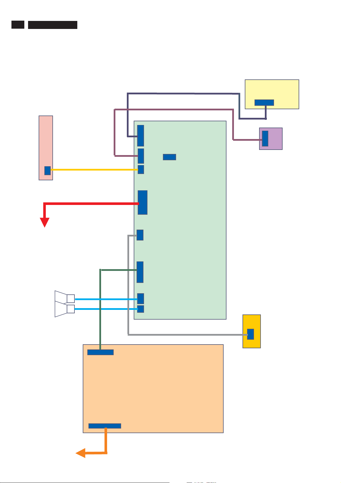
6. Block Diagram
Index of this chapter:
6.1
Wiring Diagram
6.2 Block Diagram
6.1 Wiring Diagram
1921
2p
Key board
6. Block Diagram
6
1630
8p
7
1410
8p
1M2
3
16p
1402
2p
1T1
04p
1907
6p
Side-AV
Board
Switch
board
Panel
Speakers
R/L
5.2
5.1
1
1403
30p
1M6
04p
Main Board
1001
10p
1901
3p
USB
1902
2p
8
Board
1998
4p
4
Inverter
1089
10p
1088
2
12p
Power board

Inverter
It`s Free
board
Vcc,
Bright_ADJ
Inverter ON_OFF
PWR_SAVING
SMPS board
.200W max
.PFC
.<1W at STBY
.Philips safety
rules
6. Block Diagram
PCB architecture
Control Board
S
Main BOARD
Base on TV 510 just to
modify
.DC-DC power
.Audio Amp
.inverter and panel
interface
.localize
connectors,passive
components and
memories
TPE1.0U LA
LCD Panel
26"/27"/32"
Speakers
17
S-A08
Tuner
I
IR board
IR board
IF
S-A09
HDMI
DDC
24C02
S-A04
SAW 44M
and AGC
CVI
S-A04
SAW 45.75
SAW 45.75
CVBS,YC
Audio L/R
Mains
Function block of main Board
S-A07
NXT2004
Channel decoder
(VSB/QAM
receiver)
S-A10
TDA9975A
TDA9975A
S-A02~05
PNX3000
.IF AM Demodulation
.AGC
.Video & audio switch
.I2D data link
formatter
SPDIF
16bits/H/V/CLK
Video/audio stream
MPEG2 data
UART
H/V/CL
K
RC
S-B11~14
DV1
CLK
Tunnel
bus
S-B17~22
DV4/5
PNX2015
.80C51uP
.video Decoder
AVP1
.Audio DSP
.Columbus
.MPEG Decoder (sub)
ADC
.LVDS Transmitter
S-B12
DDR x2
8Mx16?
PNX8552
.MPEG decoder
.Scaler
.DNR
.Video enhancement
.Audio delay
DV3 8 bits
I2S
A
Side AV Board
Side AV Board
I2C
RGB 30
bits,H/V/CLK
SP
I
S-B15
Nand Eeprom
Nand Eeprom
16Mx16
16Mx16
S-B15
NVM
NVM
24C64
24C64
U
USB
SPDIF
S-B12
DDR 8Mx16
DDR 8Mx16
S-B21
Flash 512K
Flash 512K
LVDS to panel
K
Key Control
Key Control
S-E27
Amp
Amp
Headphone,
speakers

18
It`s Free
S
TPE1.0U LA
PNX2015
PNX2015
Control
Control
6. Block Diagram
RESET
Reset- Stby (5V2 dip)
3V3-Standby
Reset-PNX2015
PNX2015
PNX2015
Stby uP
Stby uP
Ext Reset
Reset-system
ResetMIPS
PNX
PNX
8852
8852
EEPROM
EEPROM
ResetFE-Main
Resetaudio
NXT
NXT
2004
2004
HP/Power Amp
Anti-Plop
S
EXT
I2C
Level
Shift
PNX3000
PNX3000
TDA9975
TDA9975
PDP
SDA/SCL MM
SDA/SCL I2C4
I2C Control
PNX
PNX
2015
2015
SDA/SCL DMA
Viper
Viper
PNX8852
PNX8852
SDA/SCL
UP-VIP
EEPROM
EEPROM
NXT2004
NXT2004
SDA/SCL Tuner
Tuner
Tuner

6. Block Diagram
It`s Free
UART
S
PNX
PNX
TxD-uP
2015
2015
(Update S/W)
TPE1.0U LA
19
Factory
S
RS
232
GlinkTxD
Glink-RxD
PNX
PNX
8852
8852
PNX
PNX
2015
2015
(Factory
alignment)
(Factory
alignment)
(Update S/W)
IRQ
TxD-Viper
TxD
RxD-Viper
RxD
(For service)
RxD-uP
Switch control PNX2015uP
PNX
PNX
2015
2015
IRQ HD1
IRQ HD2
IRQ-Hirate
TDA
TDA
9975
9975
PNX
PNX
8852
8852
IRQ-Main
IRQ-MPIF
IRQ-FE-Main
PNX
PNX
3000
3000
NXT
NXT
2004
2004

20
It`s Free
P
AC input
AC input
90-264V
90-264V
TPE1.0U LA
AC
AC
LCI filter
LCI filter
6. Block Diagram
Function block of Power Board
PFC correction
PFC correction
DC 400V
DC 400V
L6562
L6562
Fly-back topology
Fly-back topology
TEA1507
TEA1507
DC+16V
DC+16V
DC+24V
DC+24V
Main Board
Main Board
.26 and 32 reuse BDS (180W max) but need <1W at Standby
""
.37 request a new one ,220W max and <1W at standby
"
Power management
P
24V
16V
DC-DC
Switch
12VS
Audio Amp
2A 12Wx2
5V2 STBY DC-
3V3-UART
DC 520mA
5V Switch 450mA
Switch (RES)
5V TUN 350mA
8V AUD
Inverter Board
Inverter Board
Inverter 6.5A for 37"
Panel 820mA for 37"
Tuner/AGC/PNX3000
PNX3000 Audio SW
PNX8852/PNX3000/HP/USB/TDA9975
3V3 DC-DC 1A
2V5 DC-DC 2A
1V2 DC-DC 3A
IR
10mA
3V3 STBY 20mA
1V2 STBY 30mA
PNX8852/PNX3000/PNX2015
PNX2015
PNX2015/PNX8852/nxt2004/TDA9975
+1V8
TDA9975
PNX2015/PNX8852/NXT2004/TDA9975/DDRs
PNX2015/PNX8852/NXT2004/DDRs
7.Circuit Diagram & PWB Layouts
It`s Free
Index of this chapter:
7.1 Chassis Overview
7.2 Exploded View
7.3 Scaler Board Schematic Diagram & Layouts
7.4 Power Board Schematic Diagram & Layouts
7.5 SIDE AV Schematic Diagram & Layouts
7.6 USB Schematic Diagram & Layouts
7.7 IR Schematic Diagram & Layouts
7.8 KEY Schematic Diagram & Layouts
Board
Board
Board
Board
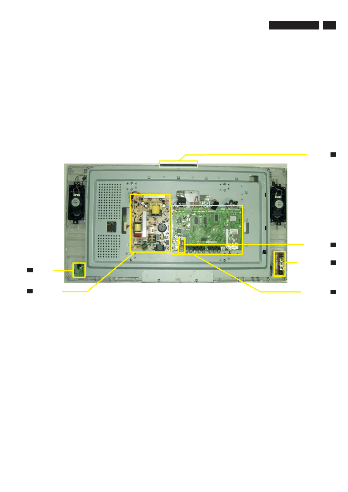
7.1 Chassi Overview
TPE1.0U LA
21
I
IR Board
Power Board
P
Key Board
USB Board
Side AV Board
Scaler Board
K
U
A
S

22
It`s Free
TPE1.0U LA
7.2 Exploded View
41
313815417421
BACK COVER
90
313815138041
MAIN SHIELD
7. Circuit Diagrams and PWB Layouts
1054
313815864901
POWER PCB ASSY- FL2 26"
7
313815758391
BASE ASSY
98
313815162031
BRACKET-AL
313815866211
USB INTERFACE PCB ASSY
301
313815760751
MAIN FRAME ASSY
823827717541
LSP 8R 5W OPN FU1R O57X126Y
1058
1185/1186
1053
313815864951
SCALER PCB ASSY - Fl2 26"
91
1050
823827718991
TFT-LCD MOD QD26HL02 REV.02
313815414931
CONTROL BUTTON
1056
313815864921
IR PCB ASSY- FL2 26"
97
313815417461
CAP
1055
313815864911
SIDE AV PCB ASSY - FL2 26"
1057
313815864971
KEY BOARD ASSY - Fl2
30
313815760741
FRONT BEZEL ASSY

7.3.1 Scaler Schematic Diagram - Block DiagramBoard
It`s Free
7.Circuit Diagrams and PWB Layouts
S-A01
TPE1.0U LA
23
24
It`s Free
TPE1.0U LA
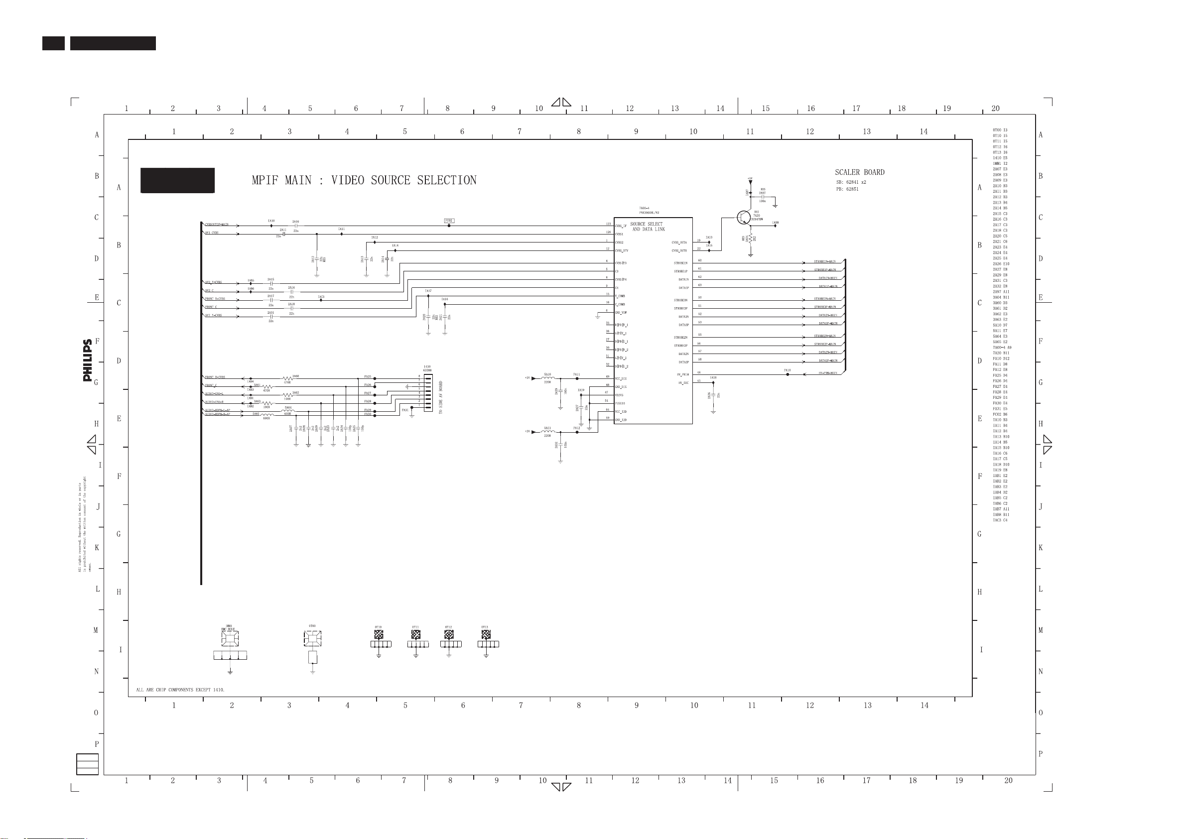
7.3.2 Scaler Schematic Diagram - MPIF MAIN: VIDEO SOURCE SELECTIONBoard
S-A02
7. Circuit Diagrams and PWB Layouts
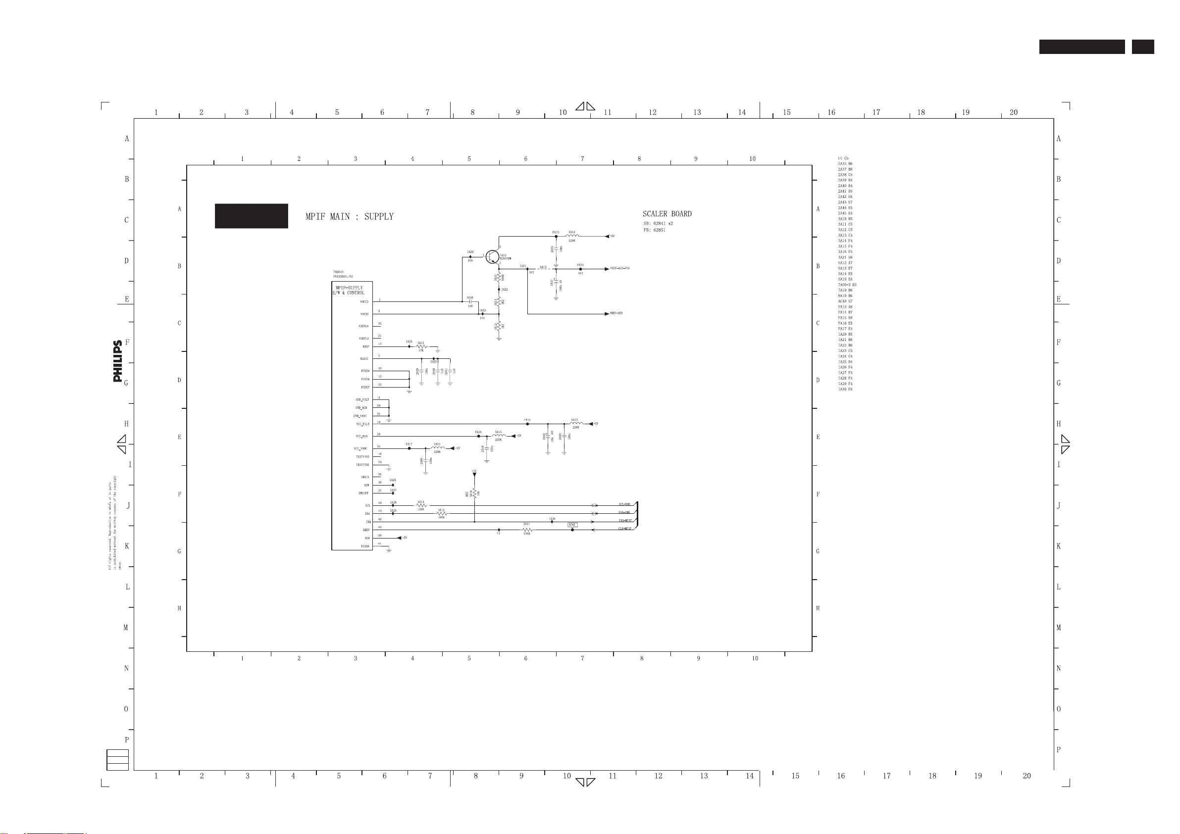
7.3.3 Scaler Schematic Diagram - MPIF MAIN: SUPPLYBoard
It`s Free
S-A03
7.Circuit Diagrams and PWB Layouts
TPE1.0U LA
25

26
It`s Free
TPE1.0U LA
7.3.4 Scaler Schematic Diagram - MPIF MAIN: IF+SAW FILTERBoard
7. Circuit Diagrams and PWB Layouts
S-A04

7.3.5 Scaler Schematic Diagram - MPIF MAIN: AUDIO SOURCE SELECTIONBoard
It`s Free
S-A05
7.Circuit Diagrams and PWB Layouts
TPE1.0U LA
27

28
It`s Free
TPE1.0U LA
7.3.6 Scaler Schematic Diagram - MPIF MAIN: AUDIO AMPLIFIERBoard
7. Circuit Diagrams and PWB Layouts
S-A06

7.3.7 Scaler Schematic Diagram - CHANNEL DECODERBoard
It`s Free
S-A07
7.Circuit Diagrams and PWB Layouts
TPE1.0U LA
29

30
It`s Free
TPE1.0U LA
7.3.8 Scaler Schematic Diagram - MAIN TUNERBoard
7. Circuit Diagrams and PWB Layouts
S-A08

7.3.9 Scaler Schematic Diagram - HDMI+SUPPLYBoard
It`s Free
S-A09
7.Circuit Diagrams and PWB Layouts
TPE1.0U LA
31

32
It`s Free
TPE1.0U LA
7.3.10 Scaler Schematic Diagram - I/O+CONTROLBoard
S-A10
7. Circuit Diagrams and PWB Layouts

7.3.11 Scaler Schematic Diagram - VIPER: CONTROLBoard
It`s Free
S-B11
7.Circuit Diagrams and PWB Layouts
TPE1.0U LA
33

34
It`s Free
TPE1.0U LA
7.3.12 Scaler Schematic Diagram - VIPER: MAIN MEMORYBoard
S-B12
7. Circuit Diagrams and PWB Layouts

7.3.13 Scaler Schematic Diagram - VIPER: A/V+TUNNELBUSBoard
It`s Free
S-B13
7.Circuit Diagrams and PWB Layouts
TPE1.0U LA
35

36
It`s Free
TPE1.0U LA
7.3.14 Scaler Schematic Diagram - VIPER: SUPPLYBoard
S-B14
7. Circuit Diagrams and PWB Layouts

7.3.15 Scaler Schematic Diagram - VIPER: EEPROMBoard
It`s Free
S-B15
7.Circuit Diagrams and PWB Layouts
TPE1.0U LA
37

38
It`s Free
TPE1.0U LA
7.3.16 Scaler Schematic Diagram - MISCELLANEOUSBoard
7. Circuit Diagrams and PWB Layouts
S-B16

7.3.17 Scaler Schematic Diagram - PNX2015: Audio/VideoBoard
It`s Free
S-B17
7.Circuit Diagrams and PWB Layouts
TPE1.0U LA
39

40
It`s Free
TPE1.0U LA
7.3.18 Scaler Schematic Diagram - PNX2015: DV I/O InterfaceBoard
7. Circuit Diagrams and PWB Layouts
S-B18

7.3.19 Scaler Schematic Diagram - PNX2015: TunnelbusBoard
It`s Free
S-B19
7.Circuit Diagrams and PWB Layouts
TPE1.0U LA
41

42
It`s Free
TPE1.0U LA
7.3.20 Scaler Schematic Diagram - PNX2015: DDR InterfaceBoard
7. Circuit Diagrams and PWB Layouts
S-B20

7.3.21 Scaler Schematic Diagram - PNX2015: Standby&ControlBoard
It`s Free
S-B21
7.Circuit Diagrams and PWB Layouts
TPE1.0U LA
43

44
It`s Free
TPE1.0U LA
7.3.22 Scaler Schematic Diagram - PNX2015: SupplyBoard
7. Circuit Diagrams and PWB Layouts
S-B22

7.3.23 Scaler Schematic Diagram - VIPER/PNX2015: Display InterfaceBoard
It`s Free
S-B23
7.Circuit Diagrams and PWB Layouts
TPE1.0U LA
45

46
It`s Free
TPE1.0U LA
7.3.24 Scaler Schematic Diagram - VIDEO-DACBoard
7. Circuit Diagrams and PWB Layouts
S-C24

7.3.25 Scaler Schematic Diagram - DC/DCBoard
It`s Free
S-D25
7.Circuit Diagrams and PWB Layouts
TPE1.0U LA
47

48
It`s Free
TPE1.0U LA
7.3.26 Scaler Schematic Diagram - SUPPLY+RS232Board
7. Circuit Diagrams and PWB Layouts
S-D26

7.3.27 Scaler Schematic Diagram - AUDIO: AMPLIFIERBoard
It`s Free
S-E27
7.Circuit Diagrams and PWB Layouts
TPE1.0U LA
49

50
It`s Free
TPE1.0U LA
7.3.28 Scaler Schematic Diagram - AUDIO: CONNECTORSBoard
7. Circuit Diagrams and PWB Layouts
S-E28

7.3.29 Scaler Schematic Diagram - ANALOG I/OBoard
It`s Free
S-F29
7.Circuit Diagrams and PWB Layouts
TPE1.0U LA
51

52
It`s Free
TPE1.0U LA
7.3.30 Scaler Board Schematic Diagram - UART
S-F30
7. Circuit Diagrams and PWB Layouts

7.3.31 Scaler Board Layouts - 1
It`s Free
S
7.Circuit Diagrams and PWB Layouts
TPE1.0U LA
53

54
It`s Free
TPE1.0U LA
7.3.31 Scaler Board Layouts - 2
S
7. Circuit Diagrams and PWB Layouts

7.4 Power Board Schematic Diagram
It`s Free
P
7.Circuit Diagrams and PWB Layouts
TPE1.0U LA
55

56
It`s Free
TPE1.0U LA
7.4 Power Board Layouts - 1
P
7. Circuit Diagrams and PWB Layouts

7.4 Power Board Layouts - 2
It`s Free
P
7.Circuit Diagrams and PWB Layouts
TPE1.0U LA
57

58
It`s Free
7.5 Side AV Board Schematic Diagram
TPE1.0U LA
7. Circuit Diagrams and PWB Layouts
A

7.5 SIDE AV Board Layouts-1
It`s Free
A
7.Circuit Diagram & PWB Layouts
TPE1.0U LA
59

60
It`s Free
7.5 SIDE AV Layouts-2Board
TPE1.0U LA
A
7. Circuit Diagrams and PWB Layouts

7.6 USB Board Schematic Diagram
It`s Free
U
7.Circuit Diagram & PWB Layouts
TPE1.0U LA
61

62
It`s Free
7.6 USB Board Layouts-1
TPE1.0U LA
U
7. Circuit Diagrams and PWB Layouts

7.6 USB Board Layouts-2
It`s Free
U
7.Circuit Diagram & PWB Layouts
TPE1.0U LA
63

64
It`s Free
7.7 IR Board Schematic Diagram
TPE1.0U LA
I
7. Circuit Diagrams and PWB Layouts

7.7 IR Board Layouts-1
It`s Free
I
7.Circuit Diagram & PWB Layouts
TPE1.0U LA
65

66
It`s Free
7.7 IR Board Layouts-2
TPE1.0U LA
I
7. Circuit Diagrams and PWB Layouts

7.8 KEY Board Schematic Diagram
It`s Free
K
7.Circuit Diagram & PWB Layouts
TPE1.0U LA
67

68
It`s Free
7.8 KEY Board Layouts-1
TPE1.0U LA
K
7. Circuit Diagrams and PWB Layouts

7.8 KEY Board Layouts-2
It`s Free
K
7.Circuit Diagram & PWB Layouts
TPE1.0U LA
69

70
It`s Free
TPE1.0U LA
8. Alignments
8. Alignments
Index of this chapter:
8.1 Electrical Instructions
8.2 Software Updrade With Portable Memory
&Serial NO. Definition
8.1 Electrical Instructions&Serial NO. Definition
1. General points
1.1 During the test and measuring, supply a distortion free AC mains
voltage to the apparatus via an isolated transformer with low
internal resistance.
1.2 All measurements mentioned hereafter are carried out at a normal
mains voltage (90 - 132 VAC for NAFTA version, 195 -264 VAC for
EUROPEAN version, or 90 - 264 VAC for the model with full range
power supply, unless otherwise stated.)
1.3 All voltages are to be measurement or applied with respect to
ground,unless otherwise stated.
1.4 The test has to be done on a complete set including LCD panel in
a room with temperature of 25 +/- 5 degree C.
1.5 All values mentioned in these test instruction are only applicable of
a well aligned apparatus, with correct signal.
1.6 The letters symbols (B) and (S) placed behind the test instruction
denotes
(B): carried out 100% inspection at assembly line
(S): carried out test by sampling
CVBS Video4 and S-Video).
Level: - Nominal : 0.5 V rms.
- Maximum : 1.5 V rms.
- Impedance > 10 kW.
2.1.2 Headphone
Audio: R/L output - 10mW at 32W. 3.5mm stereo jack with switch
Impedance is between 8 and 600W.
2.1.3 SPDIF Output (Sony Philips Digital Interface Format)
Level: - +/-0.5V square wave
2.3 TV input signal Channel and pattern for NAFTA model (Table1)
Signal Distribution Table (NTSC)
CH
A03 61.25MHz 65.75MHz NTSC M Color Circle
A06 83.25MHz 87.75MHz NTSC M Red Raster
A09 187.25MHz 191.75MHz NTSC M Circle Pattern
A11 199.25MHz 203.75MHz NTSC M Cross Hatch
A13 211.25MHz 215.75MHz NTSC M Two White Window
A52 699.25MHz 703.75MHz NTSC M Color Bar
A69 801.25MHz 805.75MHz NTSC M 100% White
C70 499.25MHz 503.75MHz NTSC M Checkerboard
Frequency Carriers
Video Sound
Table 1
TV
System
Pattern
1.7 The white balance (color temperature), has to be tested in subdued
lighted room.
1.8 Repetitive power on/off cycle are allowed except it should be
avoided within 6 sec.
2. Input and output signal
2.1 Signal definition
2.1.1 TV Signal ty pe
RF Signal : Aerial input / 10mV(80dBuV)
Video signal : Video (RCA jack, CVBS input) / 1Vpp (300mV-sync,
700mV-video.)
S video input / 1VppY-signal, 300mVpp C-signal
COMP Video (RCA jack , YPbPr input) / 1Vpp Y
signal , 350mVpp Pb , Pr signal
HDMI: Digital interface with 4 channels TMDS signal
Audio signal : Audio (1) R/L( RCA jack ) for AV IN1 (share with
CVBS Video1 and COMP Video1 or HDMI by
menu setting).
Level: - Nominal : 0.5 V rms.
- Maximum : 1.5 V rms.
- Impedance > 10 k W
Audio (2) R/L( RCA jack ) for AV IN2 (share with
CVBS Video2 and COMP Video2).
Level: - Nominal : 0.5 V rms.
- Maximum : 1.5 V rms.
- Impedance > 10 kW.
Audio (3) R/L ( RCA jack )for AV IN3 (share with
CVBS Video3 and S-Video).
Level: - Nominal : 0.5 V rms.
- Maximum : 1.5 V rms.
- Impedance > 10 k W.
Audio (4) R/L( RCA jack ) for Side AV (share with
.
2.4 HD input mode
2.4.1 HD detail timing
For QuantumData setting with Q801GD or 802G in
YpbPr mode(Table 2)
3. Power supply
3.1 Setup the AC Input at 110VAC, and power board provide two DC
Output
1. The DC output voltage is 24V ± 0.5V DC for Inverter and Scalar
board . Measure between pin3 (F026, +24V) and pin7 (F030,
GND) at item 1089 of power board with 0.1A load. Measure
between pin1 (F034, +24V) and pin8 (F039, GND) at item 1088
of power board with 4A load.
2. The DC output voltage is 16V ± 1 V DC for Scalar and Audio
board. Measure between pin2 (F025, +16V) and pin7 (F030,
GND) at item 1089 of power board with 2A load.
3. The DC voltage is 400V +/- 10V in power board. Measure
between test point F004 and ground pin of item 2060 (120uF,
450V) of power board.
3.2 No adjustment is needed.
4. IF PL L Offset Adjustm ent
A) EQUIPMENT SETUP : Fluke 54200
B) INPUT REQUIREMENTS
4.1 Input signal : M-NTSC, RF(203.25MHz, 70dBuV)
4.2 Input injection point : Tuner input.
C) ALIGNMENT METHOD
4.3 Alignment set-up: video pattern = crosshatch, sound = BTSC
stereo mode, without audio modulation, picture/sound ratio=7dB

8. Alignments
It`s Free
TPE1.0U LA
71
Item 1920X1080i
Pixel rate 74.25MHz
Horizontal
Frequency
Active 1920 pixels
Blank 280 pixels
Period 2200 pixels
Pulse delay 44 pixels
Pulse width 44 pixels
Vertical
Frequency
Active 1080 lines
Blank 45 lines
Period 1125 lines
Pulse delay 2 lines
Pulse width 5 lines
EQ before 0 line 0 line 0 line 3 line
EQ after 1 line 0 line 0 line 3 line
Scan Interlace Progressive Progressive Interlace
Sync type ACS ACS ACS ACS
Video kind Analog YPbPr
60Hz
(13.468 ns)
33.75KHz 45KHz 31.5KHz 15.734KHz
(25.859 us)
(3.771 us)
(29.630 us)
(0.593 us)
(0.593 us)
60 Hz 60 Hz 60 Hz 59.94 Hz
(32.000 ms)
(1.333 ms)
(33.333 ms)
(0.059 ms)
(0.148 ms)
(ITU-R BT.709)
1280X720P
60Hz
74.25MHz
(13.468 ns)
1280 pixels
(17.239 us)
370 pixels
(4.983 us)
1650 pixels
(22.222 us)
70 pixels
(0.943 us)
40 pixels
(0.539 us)
720 lines
(16.0 ms)
30 lines
(0.667 ms)
750 lines
(16.667 ms)
5 lines
(0.111 ms )
5 lines
(0.111 ms)
Analog YPbPr
(ITU-R BT.709)
720X480P
60Hz
27.027MHz
(37.000 ns)
720 pixels
(26.640 us)
138 pixels
(5.106 us)
858 pixels
(31.746 us)
16 pixels
(0.592 us)
62 pixels
(2.294 us)
480 lines
(15.238 ms)
45 lines
(1.429 ms)
525 lines
(16.667 ms)
9 lines
(0.287 ms)
6 lines
(0.190 ms)
Analog YPbPr
(SMPTE RP177)
720X480i
60Hz
13.5MHz
( 74.074 ns )
720 pixels
(53.333 us)
138 pixels
( 10.222 us )
858 pixels
( 63.556 us )
19 pixels
( 1.407 us )
62 pixels
( 4.593 us )
480 lines
( 30.507 ms )
45 lines
(2.860 ms )
525 lines
( 33.367 ms )
4 lines
( 0.254 ms )
3 lines
(0.191 ms )
Analog YPbPr
(SMPTE RP177 )
Table 2
4.4 Method of Alignment :
4.4.1 Set audio volume Loudspeakers to max : (+12dB avip setting)
4.4.2 Via IIC, adjust the 'PLL offset' register (address 9E, sub-address 02,
bit D5 to D0) value to get the lowest noise at audio output (I905).
4.4.3 NVM FactAlignMainIfPLLOffsetNeg at sub-address
006Chex, 1037hex, 1630hex.
5. TV Mode display adjustment
5.1 White balance adjustment (B)
5.1.1 General set-up :
Equipment Requirements: Color analyzer.
Input requirements:
Input Signal Type : RF signal
1. Set to NTSC system, frequency=187.25MHZ ( for NAFTA
model ), with white pattern of 100%
2. Select Smart picture to Personal mode and check the x, y data.
Input Signal Strength : 10mV (80 dBuV) terminal voltage.
Input Injection Point : TV Tuner input
Alignment method:
Initial Set-up :
1. Set TV Brightness=60; Contrast =95 in Factory mode.
2. Set Smart picture as "Personal"
3. Apply "100% Full White" pattern by TV pattern generator.
Alignment : Adjust the RGB White point in Factory Mode
for "NORMAL","WARM" and "COOL" color temperatures.
1. Check (X, Y) co-ordinates as below:
Picture Mode X y
Normal
WARM
COOL
Table 3: Reading with Minolta CA-110.
2. Check the gray pattern should be distinguished and color bar
is correct
Note: 1. Use Minolta CA-110 for color coordinates and
luminance check.
2. Luminance> 400 cd/m
at RGB White point set to 127 and Brightness
control; Contrast control at 100
3. Set smart picture to personal, brightness to 55 &
contrast to 95 after alignment.
7. HDMI HDCP Key
7.1 HDMI HDCP Key Test
7.1.1 Use p attern g enerator
Equipment: Quantum 802BT or equivalent equipments.
Pattern : Standard HDCP Pattern (It' s color bar)
Timing : 720 X 480i 60Hz
720 X 480P 60Hz
1280X 720P 60Hz
1920X1080i 60Hz
Result : The PASS information should be shown on the screen
0.295±0.005 0.285±0.005
0.315±0.005 0.310±0.005
0.275±0.005 0.260±0.005
2
in the center of the screen

72
It`s Free
TPE1.0U LA
8. Alignments
7.1.2 Use DVD Player:
Equipment: 1.Pioneer (model: DV-S969AVi) or equivalent
equipments.
2.DVD disk with "Macro Vision" protection.
Result : The picture should be shown Normally.
7. Preset EEPROM d ata
EEPROM data has to be preset data according following table.
7.1 Factory mode preset.
Hard ware inf o:
A. SW version: EX11U-0.5.53.1_F FL2-0.1
B. SBY PROC version: 001.008.001.010
Operatio n hour s: 0
Alignment
General
Tuner AGC: 32
Whitepoint
RedBLoffset:8
Dealer options
Personal
Ric h
Natural
Soft
Multimedia
Eco
Green Bl offset: 5
Personal option
Picture mute: On
Virgin mode: Off
Digital caption options: default
Smart Pict ure
Contrast 90
Brightness 55
Color 62
Sharpness 3
Color temperature Normal
Tint 0
Picture format Automatic
Contrast 100
Brightness 50
Color 67
Sharpness 5
Color temperature Cool
Tint 0
Picture format Automatic
Contrast 83
Brightness 50
Color 55
Sharpness 3
Color temperature Normal
Tint 0
Picture format Automatic
Contrast 83
Brightness 50
Color 55
Sharpness 1
Color temperature Normal
Tint 0
Picture format Automatic
Contrast 100
Brightness 50
Color 67
Sharpness 1
Color temperature Cool
Tint 0
Picture format Automatic
Contrast 63
Brightness 50
Color 51
Sharpness 3
Color temperature Normal
Tint 0
Picture format Automatic
Options
Display
Screen: 021 26inch LCD LPL
Scanning backlight: Off
Dimming backlight: Off
Video repro
Comb filter: 3D comb
Ambient light: Off
MOP: Off
Source selection
HDMI1: with analog audio
HDMI2: None
USB version: USB 1.1
SPDIF input: None
Audio repro
Subwoofer internal present: Off
Acoustic system: None
7.2 Smart picture & Smart sound & Feature:
7.2.1 Final TV mode out box setting.
a). Smart Picture : Personal
Color Temp in Factory mode : Normal
Notice: These setting only could modify in factory mode for
user , excluding "Personal", these menus should be blanking.
b).Smart Sound : Personal
SOUND VOLUME : 30
Balance :0
Head phone : 30
Sound mode : Stereo
Alternative audio : main
Digital audio language : English
Mono/Stereo : tbd
AVL : OFF
Delta volume: 0
EQ Setting
Personal
Speec h
Music
Movie
Multimedia
EQ BAND1 120Hz +0
EQ BAND2 500Hz +0
EQ BAND3 1.5KHz +0
EQ BAND4 5KHz +0
EQ BAND5 10KHz +0
EQ BAND1 120Hz -2
EQ BAND2 500Hz -1
EQ BAND3 1.5KHz +0
EQ BAND4 5KHz +1
EQ BAND5 10KHz +1
EQ BAND1 120Hz +2
EQ BAND2 500Hz +1
EQ BAND3 1.5KHz +1
EQ BAND4 5KHz +2
EQ BAND5 10KHz +3
EQ BAND1 120Hz +1
EQ BAND2 500Hz +0
EQ BAND3 1.5KHz +0
EQ BAND4 5KHz +1
EQ BAND5 10KHz +2
EQ BAND1 120Hz +3
EQ BAND2 500Hz +2
EQ BAND3 1.5KHz +0
EQ BAND4 5KHz +0
EQ BAND5 10KHz +0

c) .Featu res
It`s Free
Closed Captions : Off
Sleeptimer :0
8. Alignments
TPE1.0U LA
73
7.3 Setup:
7.4 Installation:
8. DDC DATA
Preferences
Picture/sound preferences
Auto surround: On
Feature preferences
Caption service: CC-1
Digital caption service: CS-1
Digital caption options: default
Menu preferences
OSD: Normal
Show emergency alert: always
..
Source
AV1: None
AV2: None
AV3: None
HDMI: None
Side: None
Analog Audio In: AV1
Clo ck
Auto clock mode: Manual
Language: English
Read the EDID data by 802BT.
Serial NO. Definition

74
It`s Free
TPE1.0U LA
8. Alignments
8.2 Software Updrade With Portable Memory
Introduction
Magnavox offers software upgrade capability for your TV using
USB portable memory (not supplied).
After you have completed a software upgrade, your TV will
typically perform better.
What improvements are made depends on the upgrade
software you are using as well as the software your TV
contained before the upgrade. You can execute the
software upgrade procedure yourself.
Be aware that the content of this document is addressing
technical or software skilled users.
Fig. 8-1
Preparing a portable memory (not supplied) for
software upgrade
For the procedure you will require:
·
A personal computer with web browsing capability.
·
An archive utility that supports the ZIP-format (e.g.
WinZip for Windowsor StuffIt for Mac OS).
·
A preferably empty USB memory stick.
Note: Only FAT/DOS-formatted portable memory is supported.
Fig. 8-3
Automatic software upgrade procedure
1. Power off your TV and remove all memory devices.
2. Insert the USB portable memory (not supplied) that contains the
downloaded software upgrade.
3. Switch on your TV with the power switch at the right side of the
TV.
4. At startup the TV will scan the USB portable memory (not
supplied) until it finds the update content. The TV will
automatically go to the upgrade mode. After a few seconds it will
display the status of the upgrade procedure.
Warning:
·
You are not allowed to remove the USB portable memory (not
supplied) during the software upgrade procedure!
·
In case of a power drop during the upgrade procedure, don t
remove the USB portable memory (not supplied) from the TV.
The TV will continue the upgrade as soon as the power comes back.
·
If you try to upgrade to a software version lower than the
current version, a confirmation will be asked. Down grading to
older software should only be done incase of real necessity.
·
If an error occurs during the upgrade, you should retry the
procedure or contact your dealer.
'
New software can be obtained from your dealer or can be
downloaded from the www.usasupport.magnavox.com web site:
Fig. 8-2
1. Go to www.usasupport.magnavox.com using the web
browser on your PC.
2. Follow the procedure to find the information and the software
related to your TV.
3. Select the latest software upgrade file and download it to your PC.
4. Decompress the ZIP-file and copy the file autorun.upg to the
root directory of the USB portable memory (not supplied).
Note: Only use software upgrades that can be found on the www.
usasupport.magnavox.com web site.
""
Verifying the version of the TV software
1. Before starting the software upgrade procedure, it is
advised to check what the current TV software is.
2. Select Software Upgrade in the Installation menu.
Press the cursor right.
The Software Upgrade menu moves to the left panel.
3. Select Current Software Info to observe the version and the
description of the current software.
Fig. 8-4
5. When the software upgrade was successful, remove the USB
portable memory (not supplied) and restart your TV with the
power switch at the right side of the TV.
Your TV will start up with the new software.
Note: Once the upgrade is finished use your PC to remove the TV
software from your USB portable memory (not supplied).
Manual software upgrade procedure
For a manual software upgrade copy the autorun.upg file in a
directory called Upgrades located in the root of the USB
portable memory (not supplied).
1. Insert the portable memory (not supplied) that contains the
downloaded software upgrade.
2. Select Software Upgrade in the Installation menu. Go to Local
upgrades/applications. The TV will list all compatible images
available on the USB portable memory (not supplied) and display
the data for each selected upgrade image.
3. Select the correct upgrade image and press the red color button to
start the upgrade. Your TV will restart and will automatically go to
the upgrade mode. After a few seconds it will display the status of
the upgrade procedure.
Warning:
If you try to upgrade to a software version equal or lower than the
current version, a confirmation will be asked. Downgrading to older
software should only be done in case of real necessity.
""
""

4. When the software upgrade was successful, remove the USB
It`s Free
portable memory (not supplied) and restart your TV with the
power switch at the right side of the TV. Your TV will start up
with the new software.
Fig. 8-5
8. Alignments
TPE1.0U LA
75

76
It`s Free
TPE1.0U LA
9. Trouble Shooting
Index of this chapter
9.1 Trouble shooting
9.2 Circuit Description
9.3 IC Data Sheets
9.4 Repair Flow Chart
9.1 Trouble Shooting
9. Trouble Shooting
Symptoms
Ghost or double
images
No power
No picture
No picture and power
switched on
Picture position
adjustment
No photo, music or
video play or in poor
quality only
No sound
Good sound but poor
color or no picture
Snowish picture and
noise
Television not
responding to
remote control
Control of accessory
devices
The software will not
install
Items to Check and Actions to follow
·
This may be caused by obstruction to the antenna due to high rise buildings or hills.
Using a highly directional antenna may improve the picture.
·
Check that the TV s AC power cord is plugged into the mains socket.
·
Unplug the television, wait for 60 seconds. Then re-insert plug into the mains socket
and turn on the television again.
·
Check antenna connections at the bottom of the TV to see if they are properly connected to the TV.
·
Possible broadcast station trouble. Try another channel.
·
Adjust the contrast and brightness settings. Try another auto picture setting.
·
Check the Closed Captions control. Some TEXT modes could block the screen.
·
Check if you selected the correct AV source.
·
Your TV has a protective mode in case there is too much heat build-up. Check the
clearance around the vents of the device to be certain there are no blocking walls or
cabinets which would limit the air flow.
When displaying a High Definition signal from the YPbPr inputs or HDMI input, if necessary, you can
adjust the picture position to the center of the screen with the cursor left/right or up/down buttons on
the remote control. This may be needed due to slight differences in output signals from different brands
and types of HD sources boxes.
Notes: Most High Definition receiver boxes also have picture-positioning controls in their menu
systems. If the TV cursor controls run out of range before the picture is correctly positoned, the
receiver box controls will need to be adjusted.
·
Check if the source complies with a supported code.
·
Increase the VOLUME.
·
Check that the TV is not muted, press the MUTE button on the remote control.
·
When no signal is detected, the TV automatically switches off the sound. This is proper
operation and does not indicate a malfunction.
·
Adjust the contrast, color, tint and brightness setting. Try another auto picture setting.
·
Check the antenna connection.
·
Check whether the batteries are working. Replace if necessary.
·
Clean the remote control sensor lens on the monitor.
·
Operating range between TV and the remote control should not be more than approximately twenty feet.
·
You can still use the buttons on the right side of your TV.
·
Check if the remote control is in the correct mode.
·
The infrared signals of the screen may influence the reception sensibility of other peripherals Solution:
replace the batteries of the remote control of other devices. E.g. keep away a wireless headphone from
within a radius of approximately four feet.
Possibly the operating system is wrong. Go to www.usasupport.magnavox.com to see which operating
systems are supported.
'
Standby
After improper
shutdown
Miscellaneous
Your TV consumes energy less than 1w in the standby mode.
Energy consumption contributes to air and water pollution.
If your TV has been shutdown in an improper way (e.g. power drop, power cord plug out), starting up the
TV again will take a longer time than usual.
See Extras, Specifications on this CD.

9. Trouble Shooting
It`s Free
TPE1.0U LA
9.2 Circuit Description
General Description
This LCD TV monitor using FL-2 platform. It can support TV signal. It's output resolution is up to 1366X768 75Hz for WXGA panel.
It can support NTSC from RF, AV0, AV1, AV2 (CVBS and Y/C), YPbPr and RGB, HDMI (DVI via HDMI) , and also have side I/O , support
CVBS/YC and Headphone for User easy used .
It can also support 640 x 480 @60p, 720 x 240 @60p, 720 x 480 @60i, 720 x 480 @60p, 800 x 600 @60p, 1280 x 720 @60p, 1024 x
768 @60p, 1920 x 1080 @60i format input.
This LCD monitor TV use MST51512 as Scaler engine, which has embedded Analog D-sub, digital DVI decoder, scaling input signal for
panel, OSD and simple 3D de-interlace. The extra SDRAM is to accomplish video frame rate conversion and PIP function.
System Description
System Description
- Signal Flows
1. Audio
2. Video
- Picture Improvement
- Power States
ATSC AV Decoding Path
77
ATSC Audio Decoding Path
ATSC Video Decoding Path(example)

78
It`s Free
Sound: PNX3000,PNX2015,PNX8550
TPE1.0U LA
9. Trouble Shooting
Picture Improvement Path
Pexel Fetch
Unit
Linear
Interpolator
Mixer
CLUT
Histogram
Modification
Contrast
Brightness
&Soft-Clip
Chroma Key
&
Undither
Luma
Sharpening
Unit
Opt.Chroma
Down-Sample
4:4:4 4:2:2
Chroma
Up-sample
Filter
Colour
Features
Gamma
Correction&
Dither
DCTI
Video/Gfx
Contrast&
Brightness
Matrix
Formatter
ABCL or
Power Meter
MUX
Horizontal
Sample-Rate
Up-convertor
Layer&
Fetch
Control

9.3 IC Data Sheets
It`s Free
9.3.1 IC Data Sheets-uPC3218GV(7T13)
9. Trouble Shooting
TPE1.0U LA
79
9.3.2 IC Data Sheets-TPA3005D2(7901)

80
It`s Free
TPE1.0U LA
9. Trouble Shooting

9.3.3 IC Data Sheets-TS482(7A04)
It`s Free
9. Trouble Shooting
TPE1.0U LA
81
9.3.4 IC Data Sheets-TDA9970A(7B50)

82
It`s Free
9.3.5 IC Data Sheets-M24C02(7B02)
Logic Diagram
9.3.6 IC Data Sheets-M24C64(7P14)
TPE1.0U LA
9. Trouble Shooting
DIP, SO and TSSOP Connections
Logic Diagram
9.3.7 IC Data Sheets-TC58DVM82F1(7P80)
PIN ASSIGNMENT
DIP, SO, TSSOP and UFDFPN Connections
BLOCK DIAGRAM

9.3.8 IC Data Sheets-LM324(7A05)
It`s Free
PIN CONFIGURATION
9.3.9 IC Data Sheets-L5972(7004)
PIN CONNECTION
9. Trouble Shooting
EQUIVALENT CIRCUIT
TEST APPLICATION CIRCUIT
TPE1.0U LA
83
9.3.10 IC Data Sheets-NCP5422A(7U00)
PIN CONNECTIONS
9.3.11 IC Data Sheets-NTX2004(7T22)
PIN ASSIGNMENTS AND DESCRIPTIONS
Application Diagram

84
It`s Free
TPE1.0U LA
9. Trouble Shooting
9.3.12 IC Data Sheets-PNX2015(7J00)
Block diagram

9. Trouble Shooting
It`s Free
TPE1.0U LA
85

86
It`s Free
TPE1.0U LA
9. Trouble Shooting
Pin configuration

9.3.13 IC Data Sheets-PNX3000(7A00)
It`s Free
Block diagram
9. Trouble Shooting
TPE1.0U LA
87

88
It`s Free
Pin Configuration
9.3.14 IC Data Sheets-PNX8552(7V00)
Block Diagram
TPE1.0U LA
9. Trouble Shooting

Pin Configuration
It`s Free
9. Trouble Shooting
TPE1.0U LA
89

90
It`s Free
TPE1.0U LA
9.4 Repair Flow Chart
9. Trouble Shooting
1.No work/LED is off
Check if
power switch is
normal
Yes
Check
power board 1089
pin1,2=16V,pin3=24V,
pin4=1.8V,pin5=
4.6V
Yes
Check scaler board1503
pin1=7V,pin3=5.2V,
pin4=4.9V,pin5=7.6V,
pin6=4.8V
2.No raster/picture too
dim
No
Replace Power switch
No
Check power board
3.No picture/LED is green
Check
power board 1088,
pin1~5=24V,pin6=
2.6V pin7=6.1V
Yes
Check if
working voltage
3Q03=3.3V,3Q27
=3.3V
Yes
Check if clock
source 1H00
Yes
No
Check power board
Check circuit around
No
each regulator and
eliminate short and
open situation
No
Replace 1H00
Check
power board 1088,
pin1~5=24V,pin6=
2.6V pin7=6.1V
Yes
Check
power board 1089
pin1,2=16V,pin3=24V,
pin4=2.6V,pin5=
6.1V
Yes
Check scaler board
No
Check power board
No
Check power board
Check if
7J00 RGB,
clk,H/V and DE signal
output 128 bits
TTL
Yes
Check
resistors-network
Yes
Replace LVDS cable
Yes
Replace LCD panel
Try to replace
No
flash Rom
EEPROM
No
Replace bad resistorsnetwork

4.No TV sound
It`s Free
Check if
tuner 1T04 pin12
output IF
signal
Yes
Check 7A11
5.No earthphone sound
Check
7814=16V
Yes
No
Replace 1T04
Eliminate short and open
No
situation
9. Trouble Shooting
6.No remote function
remote control
Check IR receiver
7.LED and function
key poor
Check circuit around
control board and cable
between control board
and scaler board
Tty another
Yes
Replace one good
No
remote control
TPE1.0U LA
91
Check 7901
pin2=ADAC2
pin6=ADAC1
Yes
Replace Side AV Board
No
Replace 7901
8.No HDMI picture
Check 7B02
has HDMI code
Yes
Check Scaler Board
Write HDMI code in
No
7B02

92
It`s Free
Model: 26MF231D/37(QDI) 12NC: 8639 000 16765
Mechanical Parts
1 313810360171 KEY BOARD
7 313815758391 BASE ASSY
30 313815760741 FRONT BEZEL ASSY
31 313815415051 BEZEL
32 313815414921 LENS-IR
33 313815414911 POWER BUTTON
41 313815417421 BACK COVER
90 313815138041 MAIN SHIELD
91 313815414931 CONTROL BUTTON
93 313815417332 GASKET
97 313815417461 CAP
98 313815162031 BRACKET-AL
99 313815415521 DOOR BASE
174 313815160891 HEATSINK
181 313815415561 IR HOLDER
182 313815415571 LED HOLDER
185 313815161801 HEAT SINK - BRIGE DIODE
187 252240189008 NUT HEX ST BLK M
191 313815161781 HEAT SINK-PW DIODE
194 313815161791 HEAT SINK-PW TRANS
197 313815321341 INSULATING PLATE
301 313815760751 MAIN FRAME ASSY
1180 313815866791 MAIN FRAME+WIRE ASSY
Packing Parts
450 313815642031 CARTON
451 313815639402 CUSHION-L
452 313815639392 CUSHION-R
453 313815640041 P.E. BAG(1000 x 600)
505 313815642031 CARTON
Accessory
145 313815524271 OWNER'S MANUAL
1172 313818870491 MAINSCORD UL 10A 1M8 DET B
miscellanea
126 313815569101 RATING LABEL
129 313810650281 P.E. BAG (INSTR. BOOK)
140 313800992021 PROCESS BOX
210 313800992011 PROCESS BOX
289 313800992011 PROCESS BOX
289 313800992061 PROCESS BOX
289 313800992061 PROCESS BOX
289 313800992061 PROCESS BOX
290 313800991961 PROCESS BOX
291 313815569131 LABEL
293 313815569161 LABEL
300 282206240595 INK CARTRIDGE -EP-T
615 313811709281 HEX CODE OF F/W(NO MATL REQ)
615 313811709381 HEX CODE OF F/W(NO MATL REQ)
1176 313923812851 PROD ASSY RC1113125/00B PKD
1185 823827717541 LSP 8R 5W OPN FU1R O57X126Y
1186 823827717541 LSP 8R 5W OPN FU1R O57X126Y
1251 313815859171 DIODE ASSY GBU6J 6051
1252 313815859181 DIODE ASSY STTH5L06 6052
1253 313815859191 DIODE ASSY( 6071,6076)
1254 313815859211 POW TRANS ASSY 7057/ 7062
4444 313810650020 CD ROM - SERVICE MANUAL
8001 313819874741 CBLE-390 10/110/10-020 AWG26
8088 823827732033 CBLE-392 12/230/14-024 AWG26
8402 823827732031 CBLE-001 2/445/2-012 AWG28
8403 823827732034 CBLE-130 30/220/30-033 AWG28
8410 823827732035 CBLE-018 8/480/8-388 AWG28
8901 823827732028 CBLE FAST/555/2-392 AWG26
8902 823827732029 CBLE FAST/555/3 -123 AWG26
8M21 823827732032 CBLE-016 6/830/6-016 AWG28
8M60 823827732036 CBLE-014 4/200/4-014 AWG28
LCD Panel
1050 823827718991 TFT-LCD MOD QD26HL02 REV.02
PCB Assy
1053 313815864951 SCALER PCB ASSY - FL2 26"
1054 313815864901 POWER PCB ASSY- FL2 26"
1055 313815864911 SIDE AV PCB ASSY - FL2 26"
1056 313815864921 IR PCB ASSY- FL2 26"
1057 313815864971 KEY BOARD ASSY - FL2
1058 313815866211 USB INTERFACE PCB ASSY
PCB Assy
1053 313815864951 SCALER PCB ASSY - FL2 26"
TPE1.0U LA
10.Spare Parts List
Various
1001 242202518823 CON V 10P M 2.00 63390
1402 242202518814 CON V 2P M 2.00 63382
1403 242202518804 CON V 30P M 1.25 SM 60948
1410 242202518821 CON V 8P M 2.00 63388
1902 242202518814 CON V 2P M 2.00 63382
1A10 242254944377 FIL SAW SM 45MHZ75 OFWM1967L
1H00 242254301397 RES XTL SM 27MHZ 18P DSX840
1H07 242202503999 CON V 14P M 2.54 SM 147279
1I00 823827733007 RCA JACK 2X2(WRBY)
1I01 243803100431 SOC MDIN H 4P F 69015
1I03 823827733006 RCA JACK 3X2(RBGWRY)
1I04 823827733006 RCA JACK 3X2(RBGWRY)
1I06 242203300018 SOC HDMI H 19P F SM FLANGE
1LA0 242254301443 RES XTL SM 16MHZ 20P DSX840
1M16 823827733005 CON BM H 3P M 2.0 62283
1M21 242202518818 CON V 6P M 2.00 63386
1M60 242202518816 CON V 4P M 2.00 63384
1T01 242254900137 FIL SAW SM 44MHZ X7351P
1T04 311229714221 TUNER TD1336O/FGHP
1T11 242254301506 RES XTL SM 25M14 20P NX8045
1U01 242208600623 FUSE SM T 3A 125V UL
2001 223858115649 CER2 1206 X7R 50V 100N PM10
2002 823827736021 ELCAP SM VEJ 25V S 100U PM20
2006 823827736023 ELCAP SM VGA 16V S 1000U PM20
2007 823827736022 ELCAP SM VEJ 35V S 47U PM20 R
2008 223858115649 CER2 1206 X7R 50V 100N PM10
2009 223886775221 CER1 0603 NP0 50V 220P PM5
2010 223858655641 CER2 0603 X7R 50V 22N PM10
2011 823827736023 ELCAP SM VGA 16V S 1000U PM20
2014 223858615614 CER2 0603 X7R 50V 220P PM10
2015 223858619807 CER2 0603 Y5V 50V 22N P8020
2406 223878619854 CER2 0603 Y5V 16V 220N P8020
2407 222224119876 CER2 1206 Y5V 10V 10U P8020
2421 222224119876 CER2 1206 Y5V 10V 10U P8020
2501 222224119876 CER2 1206 Y5V 10V 10U P8020
2502 202255205893 CER2 0402 X7R 16V 10N PM10
2503 223886715568 CER1 0603 NP0 50V 5P6 PM0P5
2504 223886715568 CER1 0603 NP0 50V 5P6 PM0P5
2505 223858615623 CER2 0603 X7R 50V 1N PM10
2506 223858615623 CER2 0603 X7R 50V 1N PM10
2507 223886715308 CER1 0603 NP0 50V 3P PM0P25
2508 223878615649 CER2 0603 X7R 16V 100N PM10
2901 823827736011 ELCAP RXW 25V S 1000U PM20 B
2902 222291016649 CER2 0805 X7R 25V 100N PM10
2903 823827736011 ELCAP RXW 25V S 1000U PM20 B
2904 223858615636 CER2 0603 X7R 50V 10N PM10
2908 202001293726 ELCAP SM RV 25V 100U PM20
2909 223891615649 CER2 0603 X7R 25V 100N PM10
2910 223891615649 CER2 0603 X7R 25V 100N PM10
2911 223891615649 CER2 0603 X7R 25V 100N PM10
2912 223891615649 CER2 0603 X7R 25V 100N PM10
2913 202001293726 ELCAP SM RV 25V 100U PM20
2914 202001293782 ELCAP SM RV2 25V 10U PM20
2915 223886775221 CER1 0603 NP0 50V 220P PM5
2916 223878619854 CER2 0603 Y5V 16V 220N P8020
2917 223878619854 CER2 0603 Y5V 16V 220N P8020
2918 223878619854 CER2 0603 Y5V 16V 220N P8020
2919 223878619854 CER2 0603 Y5V 16V 220N P8020
2920 223878619854 CER2 0603 Y5V 16V 220N P8020
2921 202203100242 ELCAP SM RVS 50V 1U PM20
2922 202203100242 ELCAP SM RVS 50V 1U PM20
2923 222258015649 CER2 0805 X7R 50V 100N PM10
2924 823827736029 CER2 0603 X7R 16V 220N PM10 R
2925 823827736031 CER2 1206 X7R 50V 470N PM10 R
2926 823827736029 CER2 0603 X7R 16V 220N PM10 R
2927 223886775101 CER1 0603 NP0 50V 100P PM5
2928 223886775101 CER1 0603 NP0 50V 100P PM5
2929 223878615649 CER2 0603 X7R 16V 100N PM10
2930 223878615649 CER2 0603 X7R 16V 100N PM10
2931 223886775101 CER1 0603 NP0 50V 100P PM5
2932 823827736029 CER2 0603 X7R 16V 220N PM10 R
2933 223878615649 CER2 0603 X7R 16V 100N PM10
2934 223891615649 CER2 0603 X7R 25V 100N PM10
2935 223886775101 CER1 0603 NP0 50V 100P PM5
2936 823827736031 CER2 1206 X7R 50V 470N PM10 R
2937 823827736029 CER2 0603 X7R 16V 220N PM10 R
2938 223858115649 CER2 1206 X7R 50V 100N PM10
2A07 223858715627 CER2 0402 X7R 50V 2N2 PM10
2A08 223858715627 CER2 0402 X7R 50V 2N2 PM10
2A09 223858715627 CER2 0402 X7R 50V 2N2 PM10
2A10 223878715641 CER2 0402 X7R 16V 22N PM10
2A11 223878715641 CER2 0402 X7R 16V 22N PM10
2A13 223878715641 CER2 0402 X7R 16V 22N PM10
2A14 223878715641 CER2 0402 X7R 16V 22N PM10
2A15 223878715641 CER2 0402 X7R 16V 22N PM10
2A16 223878715641 CER2 0402 X7R 16V 22N PM10
2A17 223878715641 CER2 0402 X7R 16V 22N PM10
2A18 223878715641 CER2 0402 X7R 16V 22N PM10
2A19 202255205893 CER2 0402 X7R 16V 10N PM10
2A21 223878715641 CER2 0402 X7R 16V 22N PM10
2A23 223858715627 CER2 0402 X7R 50V 2N2 PM10
2A24 223886975101 CER1 0402 NP0 50V 100P PM5
2A25 223886975101 CER1 0402 NP0 50V 100P PM5
2A26 223878715641 CER2 0402 X7R 16V 22N PM10
2A27 223878715641 CER2 0402 X7R 16V 22N PM10
2A29 223878615649 CER2 0603 X7R 16V 100N PM10
2A31 223878715641 CER2 0402 X7R 16V 22N PM10
2A32 223878615649 CER2 0603 X7R 16V 100N PM10
2A33 222278015663 CER2 0805 X7R 16V 1U PM10
2A34 222278015663 CER2 0805 X7R 16V 1U PM10
2A35 223878615649 CER2 0603 X7R 16V 100N PM10
2A37 202202000752 ELCAP SM RV2 4V 100U PM20
2A38 223858715623 CER2 0402 X7R 50V 1N PM10
2A39 223878615649 CER2 0603 X7R 16V 100N PM10
2A40 222278015663 CER2 0805 X7R 16V 1U PM10
2A41 222278015663 CER2 0805 X7R 16V 1U PM10
2A42 202202000756 ELCAP SM RV2 16V 10U PM20
2A43 223878615649 CER2 0603 X7R 16V 100N PM10
2A44 223878615649 CER2 0603 X7R 16V 100N PM10
2A45 223878615649 CER2 0603 X7R 16V 100N PM10
2A47 223878615649 CER2 0603 X7R 16V 100N PM10
2A49 202255205893 CER2 0402 X7R 16V 10N PM10
2A50 202255205893 CER2 0402 X7R 16V 10N PM10
2A51 223858715616 CER2 0402 X7R 50V 330P PM10
2A52 223878615649 CER2 0603 X7R 16V 100N PM10
2A53 202255205893 CER2 0402 X7R 16V 10N PM10
2A54 202255205893 CER2 0402 X7R 16V 10N PM10
2A55 202255205893 CER2 0402 X7R 16V 10N PM10
2A56 222278015663 CER2 0805 X7R 16V 1U PM10
2A57 222278015663 CER2 0805 X7R 16V 1U PM10
2A58 202255205893 CER2 0402 X7R 16V 10N PM10
2A60 222278015663 CER2 0805 X7R 16V 1U PM10
2A61 222278015663 CER2 0805 X7R 16V 1U PM10
2A62 223878615649 CER2 0603 X7R 16V 100N PM10
2A63 223878615649 CER2 0603 X7R 16V 100N PM10
2A64 223878615649 CER2 0603 X7R 16V 100N PM10
2A65 223878615649 CER2 0603 X7R 16V 100N PM10
2A66 222278015663 CER2 0805 X7R 16V 1U PM10
2A67 222278015663 CER2 0805 X7R 16V 1U PM10
2A68 222278015663 CER2 0805 X7R 16V 1U PM10
2A69 222278015663 CER2 0805 X7R 16V 1U PM10
2A71 222278015663 CER2 0805 X7R 16V 1U PM10
2A73 222278015663 CER2 0805 X7R 16V 1U PM10
2A76 222278015663 CER2 0805 X7R 16V 1U PM10
2A78 202001293803 ELCAP SM RV2 16V 100U PM20
2A79 223886975339 CER1 0402 NP0 50V 33P PM5
2A81 223878615649 CER2 0603 X7R 16V 100N PM10
2A83 202202000902 ELCAP SM LV 16V 100U PM20
2A84 223886975339 CER1 0402 NP0 50V 33P PM5
2A86 223858715623 CER2 0402 X7R 50V 1N PM10
2A87 222278015663 CER2 0805 X7R 16V 1U PM10
2A90 202255205893 CER2 0402 X7R 16V 10N PM10
2A92 222278015663 CER2 0805 X7R 16V 1U PM10
2B00 223878615649 CER2 0603 X7R 16V 100N PM10
2B01 223878615649 CER2 0603 X7R 16V 100N PM10
2B03 223891715632 CER2 0402 X7R 25V 4N7 PM10
2B04 202255205893 CER2 0402 X7R 16V 10N PM10
2B10 223878615649 CER2 0603 X7R 16V 100N PM10
2B11 202202000751 ELCAP SM RV2 4V 47U PM20
2B12 223878615649 CER2 0603 X7R 16V 100N PM10
2B13 223878615649 CER2 0603 X7R 16V 100N PM10
2B14 223878615649 CER2 0603 X7R 16V 100N PM10
2B15 223878615649 CER2 0603 X7R 16V 100N PM10
2B16 223878615649 CER2 0603 X7R 16V 100N PM10
2B17 223878615649 CER2 0603 X7R 16V 100N PM10
2B18 223878615649 CER2 0603 X7R 16V 100N PM10
2B19 223878615649 CER2 0603 X7R 16V 100N PM10
2B20 223878615649 CER2 0603 X7R 16V 100N PM10
2B21 223878615649 CER2 0603 X7R 16V 100N PM10
2B22 223878615649 CER2 0603 X7R 16V 100N PM10
2B23 223878615649 CER2 0603 X7R 16V 100N PM10
2B24 223878615649 CER2 0603 X7R 16V 100N PM10
2B25 223878615649 CER2 0603 X7R 16V 100N PM10
2B26 223878615649 CER2 0603 X7R 16V 100N PM10
2B31 202255205893 CER2 0402 X7R 16V 10N PM10
2B32 223878615649 CER2 0603 X7R 16V 100N PM10
2B33 223878615649 CER2 0603 X7R 16V 100N PM10
2B35 223878615649 CER2 0603 X7R 16V 100N PM10
2B36 223878615649 CER2 0603 X7R 16V 100N PM10
2B37 223878615649 CER2 0603 X7R 16V 100N PM10
2B38 223878615649 CER2 0603 X7R 16V 100N PM10
2B39 223878615649 CER2 0603 X7R 16V 100N PM10
2B40 202202000752 ELCAP SM RV2 4V 100U PM20
2B41 202202000752 ELCAP SM RV2 4V 100U PM20
2B45 222278015663 CER2 0805 X7R 16V 1U PM10
2B46 222278015663 CER2 0805 X7R 16V 1U PM10
2B50 202255205893 CER2 0402 X7R 16V 10N PM10
2B51 202255205893 CER2 0402 X7R 16V 10N PM10
2B52 202255205893 CER2 0402 X7R 16V 10N PM10
2B55 202255205893 CER2 0402 X7R 16V 10N PM10

2B56 223886915158 CER1 0402 NP0 50V 1P5 PM0P25
It`s Free
2B57 223886915109 CER1 0402 NP0 50V 10P PM5
2B58 202255205893 CER2 0402 X7R 16V 10N PM10
2B59 223886915158 CER1 0402 NP0 50V 1P5 PM0P25
2B60 223886915109 CER1 0402 NP0 50V 10P PM5
2B61 202255205893 CER2 0402 X7R 16V 10N PM10
2B62 223886915158 CER1 0402 NP0 50V 1P5 PM0P25
2B63 223886915109 CER1 0402 NP0 50V 10P PM5
2B64 202255205893 CER2 0402 X7R 16V 10N PM10
2B65 223886915158 CER1 0402 NP0 50V 1P5 PM0P25
2B66 223886915109 CER1 0402 NP0 50V 10P PM5
2B67 202255205893 CER2 0402 X7R 16V 10N PM10
2B68 223886915158 CER1 0402 NP0 50V 1P5 PM0P25
2B69 223886915109 CER1 0402 NP0 50V 10P PM5
2B70 202255205893 CER2 0402 X7R 16V 10N PM10
2B71 223886915158 CER1 0402 NP0 50V 1P5 PM0P25
2B72 223886915109 CER1 0402 NP0 50V 10P PM5
2B75 202255205893 CER2 0402 X7R 16V 10N PM10
2B76 202255205893 CER2 0402 X7R 16V 10N PM10
2B77 202255205893 CER2 0402 X7R 16V 10N PM10
2B78 202255205893 CER2 0402 X7R 16V 10N PM10
2B79 202255205893 CER2 0402 X7R 16V 10N PM10
2B80 202255205893 CER2 0402 X7R 16V 10N PM10
2G35 223878615649 CER2 0603 X7R 16V 100N PM10
2H00 223886975101 CER1 0402 NP0 50V 100P PM5
2H01 223858715623 CER2 0402 X7R 50V 1N PM10
2H02 223878615649 CER2 0603 X7R 16V 100N PM10
2H03 222278015663 CER2 0805 X7R 16V 1U PM10
2H06 223858715623 CER2 0402 X7R 50V 1N PM10
2H07 223858715623 CER2 0402 X7R 50V 1N PM10
2H08 223886915279 CER1 0402 NP0 50V 27P PM5
2H09 223886915279 CER1 0402 NP0 50V 27P PM5
2H10 223878615649 CER2 0603 X7R 16V 100N PM10
2H11 223886975101 CER1 0402 NP0 50V 100P PM5
2H12 222278015663 CER2 0805 X7R 16V 1U PM10
2I02 223886975101 CER1 0402 NP0 50V 100P PM5
2I03 223886975101 CER1 0402 NP0 50V 100P PM5
2I05 223886975101 CER1 0402 NP0 50V 100P PM5
2I06 223886975101 CER1 0402 NP0 50V 100P PM5
2I07 223886975101 CER1 0402 NP0 50V 100P PM5
2I08 223886975101 CER1 0402 NP0 50V 100P PM5
2I09 223886975129 CER1 0402 NP0 50V 12P PM5
2I0E 223886975101 CER1 0402 NP0 50V 100P PM5
2I0F 223886975101 CER1 0402 NP0 50V 100P PM5
2I53 223878615649 CER2 0603 X7R 16V 100N PM10
2J01 223878615649 CER2 0603 X7R 16V 100N PM10
2J03 223878615649 CER2 0603 X7R 16V 100N PM10
2J06 223878615649 CER2 0603 X7R 16V 100N PM10
2J08 223878615649 CER2 0603 X7R 16V 100N PM10
2J10 223878615649 CER2 0603 X7R 16V 100N PM10
2J13 223878615649 CER2 0603 X7R 16V 100N PM10
2J16 223878615649 CER2 0603 X7R 16V 100N PM10
2J18 223878615649 CER2 0603 X7R 16V 100N PM10
2J20 223878615649 CER2 0603 X7R 16V 100N PM10
2J57 223878615649 CER2 0603 X7R 16V 100N PM10
2J76 222278015663 CER2 0805 X7R 16V 1U PM10
2L01 223858715623 CER2 0402 X7R 50V 1N PM10
2L06 222278015663 CER2 0805 X7R 16V 1U PM10
2L07 223878615649 CER2 0603 X7R 16V 100N PM10
2L08 223878615649 CER2 0603 X7R 16V 100N PM10
2L50 223878615649 CER2 0603 X7R 16V 100N PM10
2L51 223878615649 CER2 0603 X7R 16V 100N PM10
2L52 223878615649 CER2 0603 X7R 16V 100N PM10
2L53 223878615649 CER2 0603 X7R 16V 100N PM10
2L54 223878615649 CER2 0603 X7R 16V 100N PM10
2L55 223858715623 CER2 0402 X7R 50V 1N PM10
2L56 223878615649 CER2 0603 X7R 16V 100N PM10
2L57 223878615649 CER2 0603 X7R 16V 100N PM10
2L58 223878615649 CER2 0603 X7R 16V 100N PM10
2L59 223858715623 CER2 0402 X7R 50V 1N PM10
2L60 223878615649 CER2 0603 X7R 16V 100N PM10
2L61 223858715623 CER2 0402 X7R 50V 1N PM10
2L62 223858715623 CER2 0402 X7R 50V 1N PM10
2L63 223886975101 CER1 0402 NP0 50V 100P PM5
2L64 223858715623 CER2 0402 X7R 50V 1N PM10
2L65 223858715629 CER2 0402 X7R 50V 3N3 PM10
2L66 223858715629 CER2 0402 X7R 50V 3N3 PM10
2L80 225020013667 CER2 0805 X5R 6V3 2U2 PM10
2L81 225020013667 CER2 0805 X5R 6V3 2U2 PM10
2L82 225020013667 CER2 0805 X5R 6V3 2U2 PM10
2L83 225020013667 CER2 0805 X5R 6V3 2U2 PM10
2L84 223878615649 CER2 0603 X7R 16V 100N PM10
2L85 223878615649 CER2 0603 X7R 16V 100N PM10
2L86 223878615649 CER2 0603 X7R 16V 100N PM10
2L87 223878615649 CER2 0603 X7R 16V 100N PM10
2L88 223886975101 CER1 0402 NP0 50V 100P PM5
2L89 223858715623 CER2 0402 X7R 50V 1N PM10
2L90 223858715623 CER2 0402 X7R 50V 1N PM10
2L91 223858715623 CER2 0402 X7R 50V 1N PM10
2L92 223858715623 CER2 0402 X7R 50V 1N PM10
2LA0 223886915229 CER1 0402 NP0 50V 22P PM5
10.Spare Parts List
2LA1 223886915229 CER1 0402 NP0 50V 22P PM5
2LA2 223886915109 CER1 0402 NP0 50V 10P PM5
2LA4 223878615649 CER2 0603 X7R 16V 100N PM10
2LA5 223858715629 CER2 0402 X7R 50V 3N3 PM10
2LA6 223858715629 CER2 0402 X7R 50V 3N3 PM10
2LA8 223858715629 CER2 0402 X7R 50V 3N3 PM10
2LA9 223858715629 CER2 0402 X7R 50V 3N3 PM10
2LB0 223878615649 CER2 0603 X7R 16V 100N PM10
2LB1 223878615649 CER2 0603 X7R 16V 100N PM10
2LB3 223858715623 CER2 0402 X7R 50V 1N PM10
2LB4 223878615649 CER2 0603 X7R 16V 100N PM10
2LN2 202202000751 ELCAP SM RV2 4V 47U PM20
2LN3 223878615649 CER2 0603 X7R 16V 100N PM10
2LN4 223878615649 CER2 0603 X7R 16V 100N PM10
2LN5 223878615649 CER2 0603 X7R 16V 100N PM10
2LN6 223878615649 CER2 0603 X7R 16V 100N PM10
2LN7 223878615649 CER2 0603 X7R 16V 100N PM10
2LN8 223878615649 CER2 0603 X7R 16V 100N PM10
2LP0 202202000752 ELCAP SM RV2 4V 100U PM20
2LP2 223878615649 CER2 0603 X7R 16V 100N PM10
2LP3 223878615649 CER2 0603 X7R 16V 100N PM10
2LP4 223878615649 CER2 0603 X7R 16V 100N PM10
2LP7 202202000752 ELCAP SM RV2 4V 100U PM20
2LP8 223878615649 CER2 0603 X7R 16V 100N PM10
2LP9 223878615649 CER2 0603 X7R 16V 100N PM10
2LR0 223878615649 CER2 0603 X7R 16V 100N PM10
2LR2 223878615649 CER2 0603 X7R 16V 100N PM10
2LR4 223878615649 CER2 0603 X7R 16V 100N PM10
2LR5 223878615649 CER2 0603 X7R 16V 100N PM10
2LR6 223878615649 CER2 0603 X7R 16V 100N PM10
2LR8 223878615649 CER2 0603 X7R 16V 100N PM10
2LR9 223878615649 CER2 0603 X7R 16V 100N PM10
2LS5 223878615649 CER2 0603 X7R 16V 100N PM10
2LT0 222278015663 CER2 0805 X7R 16V 1U PM10
2M80 223878615649 CER2 0603 X7R 16V 100N PM10
2M81 223886975101 CER1 0402 NP0 50V 100P PM5
2M83 223886975101 CER1 0402 NP0 50V 100P PM5
2M84 223886975101 CER1 0402 NP0 50V 100P PM5
2M91 202255205893 CER2 0402 X7R 16V 10N PM10
2M92 222278015663 CER2 0805 X7R 16V 1U PM10
2M93 202255205893 CER2 0402 X7R 16V 10N PM10
2M94 222278015663 CER2 0805 X7R 16V 1U PM10
2P34 223878615649 CER2 0603 X7R 16V 100N PM10
2P35 223878615649 CER2 0603 X7R 16V 100N PM10
2P80 223878615649 CER2 0603 X7R 16V 100N PM10
2P81 223878615649 CER2 0603 X7R 16V 100N PM10
2Q01 222278015663 CER2 0805 X7R 16V 1U PM10
2Q03 222278015663 CER2 0805 X7R 16V 1U PM10
2Q04 223878615649 CER2 0603 X7R 16V 100N PM10
2Q05 223878615649 CER2 0603 X7R 16V 100N PM10
2Q06 223878615649 CER2 0603 X7R 16V 100N PM10
2Q07 223878615649 CER2 0603 X7R 16V 100N PM10
2Q08 223878615649 CER2 0603 X7R 16V 100N PM10
2Q09 223878615649 CER2 0603 X7R 16V 100N PM10
2Q10 223878615649 CER2 0603 X7R 16V 100N PM10
2Q11 223878615649 CER2 0603 X7R 16V 100N PM10
2Q12 223878615649 CER2 0603 X7R 16V 100N PM10
2Q13 223878615649 CER2 0603 X7R 16V 100N PM10
2Q14 223878615649 CER2 0603 X7R 16V 100N PM10
2Q15 223878615649 CER2 0603 X7R 16V 100N PM10
2Q16 202255205893 CER2 0402 X7R 16V 10N PM10
2Q17 202255205893 CER2 0402 X7R 16V 10N PM10
2Q18 202255205893 CER2 0402 X7R 16V 10N PM10
2Q19 202255205893 CER2 0402 X7R 16V 10N PM10
2Q20 823827736027 CER2 0805 X7R 10V 4U7 PM10 R
2Q21 222278015663 CER2 0805 X7R 16V 1U PM10
2Q22 823827736027 CER2 0805 X7R 10V 4U7 PM10 R
2Q23 222278015663 CER2 0805 X7R 16V 1U PM10
2Q24 223878615649 CER2 0603 X7R 16V 100N PM10
2Q26 223878615649 CER2 0603 X7R 16V 100N PM10
2Q27 223878615649 CER2 0603 X7R 16V 100N PM10
2Q28 223878615649 CER2 0603 X7R 16V 100N PM10
2Q30 223878615649 CER2 0603 X7R 16V 100N PM10
2Q32 223878615649 CER2 0603 X7R 16V 100N PM10
2Q33 223878615649 CER2 0603 X7R 16V 100N PM10
2Q34 223878615649 CER2 0603 X7R 16V 100N PM10
2Q35 223878615649 CER2 0603 X7R 16V 100N PM10
2Q37 223878615649 CER2 0603 X7R 16V 100N PM10
2Q38 223878615649 CER2 0603 X7R 16V 100N PM10
2Q39 223878615649 CER2 0603 X7R 16V 100N PM10
2Q42 823827736027 CER2 0805 X7R 10V 4U7 PM10 R
2Q43 823827736027 CER2 0805 X7R 10V 4U7 PM10 R
2Q44 223878615649 CER2 0603 X7R 16V 100N PM10
2Q45 223878615649 CER2 0603 X7R 16V 100N PM10
2Q46 223878615649 CER2 0603 X7R 16V 100N PM10
2Q47 223878615649 CER2 0603 X7R 16V 100N PM10
2Q48 223878615649 CER2 0603 X7R 16V 100N PM10
2Q49 223878615649 CER2 0603 X7R 16V 100N PM10
2Q50 223878615649 CER2 0603 X7R 16V 100N PM10
2Q51 223878615649 CER2 0603 X7R 16V 100N PM10
2Q52 223878615649 CER2 0603 X7R 16V 100N PM10
TPE1.0U LA
2Q53 223878615649 CER2 0603 X7R 16V 100N PM10
2Q54 223878615649 CER2 0603 X7R 16V 100N PM10
2Q55 223878615649 CER2 0603 X7R 16V 100N PM10
2Q56 202255205893 CER2 0402 X7R 16V 10N PM10
2Q57 202255205893 CER2 0402 X7R 16V 10N PM10
2Q58 202255205893 CER2 0402 X7R 16V 10N PM10
2Q59 202255205893 CER2 0402 X7R 16V 10N PM10
2Q60 223878615649 CER2 0603 X7R 16V 100N PM10
2Q61 223858715623 CER2 0402 X7R 50V 1N PM10
2Q62 223886975101 CER1 0402 NP0 50V 100P PM5
2Q63 223878615649 CER2 0603 X7R 16V 100N PM10
2Q64 223878615649 CER2 0603 X7R 16V 100N PM10
2Q65 223878615649 CER2 0603 X7R 16V 100N PM10
2Q66 223878615649 CER2 0603 X7R 16V 100N PM10
2Q67 223858715623 CER2 0402 X7R 50V 1N PM10
2Q69 202203100371 ELCAP SM RV 16V 470U PM20
2Q70 223886975101 CER1 0402 NP0 50V 100P PM5
2Q71 223886975101 CER1 0402 NP0 50V 100P PM5
2Q76 223858715623 CER2 0402 X7R 50V 1N PM10
2Q77 223858715623 CER2 0402 X7R 50V 1N PM10
2Q82 823827736027 CER2 0805 X7R 10V 4U7 PM10 R
2Q83 823827736027 CER2 0805 X7R 10V 4U7 PM10 R
2Q84 202255205893 CER2 0402 X7R 16V 10N PM10
2Q85 202255205893 CER2 0402 X7R 16V 10N PM10
2Q86 202255205893 CER2 0402 X7R 16V 10N PM10
2Q87 223858715623 CER2 0402 X7R 50V 1N PM10
2Q88 223858715623 CER2 0402 X7R 50V 1N PM10
2Q89 223858715623 CER2 0402 X7R 50V 1N PM10
2Q90 223858715623 CER2 0402 X7R 50V 1N PM10
2Q91 202255205893 CER2 0402 X7R 16V 10N PM10
2T10 202255205893 CER2 0402 X7R 16V 10N PM10
2T11 202255205893 CER2 0402 X7R 16V 10N PM10
2T12 202255205893 CER2 0402 X7R 16V 10N PM10
2T13 202255205893 CER2 0402 X7R 16V 10N PM10
2T14 202255205893 CER2 0402 X7R 16V 10N PM10
2T15 202255205893 CER2 0402 X7R 16V 10N PM10
2T16 222278015663 CER2 0805 X7R 16V 1U PM10
2T17 202255205893 CER2 0402 X7R 16V 10N PM10
2T18 202255205893 CER2 0402 X7R 16V 10N PM10
2T19 202255205893 CER2 0402 X7R 16V 10N PM10
2T20 202255205893 CER2 0402 X7R 16V 10N PM10
2T21 202255205893 CER2 0402 X7R 16V 10N PM10
2T22 202255205893 CER2 0402 X7R 16V 10N PM10
2T23 223878615649 CER2 0603 X7R 16V 100N PM10
2T24 222224119876 CER2 1206 Y5V 10V 10U P8020
2T25 202255205893 CER2 0402 X7R 16V 10N PM10
2T26 223886915181 CER1 0402 NP0 50V 180P PM5
2T27 223886915181 CER1 0402 NP0 50V 180P PM5
2T30 202255205893 CER2 0402 X7R 16V 10N PM10
2T31 202255205893 CER2 0402 X7R 16V 10N PM10
2T33 202255205893 CER2 0402 X7R 16V 10N PM10
2T34 202255205893 CER2 0402 X7R 16V 10N PM10
2T35 202255205893 CER2 0402 X7R 16V 10N PM10
2T36 223878615649 CER2 0603 X7R 16V 100N PM10
2T37 223878615649 CER2 0603 X7R 16V 100N PM10
2T38 223878615649 CER2 0603 X7R 16V 100N PM10
2T39 223878615649 CER2 0603 X7R 16V 100N PM10
2T40 223878615649 CER2 0603 X7R 16V 100N PM10
2T41 223878615649 CER2 0603 X7R 16V 100N PM10
2T42 223878615649 CER2 0603 X7R 16V 100N PM10
2T43 223878615649 CER2 0603 X7R 16V 100N PM10
2T44 223878615649 CER2 0603 X7R 16V 100N PM10
2T45 223878615649 CER2 0603 X7R 16V 100N PM10
2T46 223878615649 CER2 0603 X7R 16V 100N PM10
2T47 223878615649 CER2 0603 X7R 16V 100N PM10
2T48 223878615649 CER2 0603 X7R 16V 100N PM10
2T49 223878615649 CER2 0603 X7R 16V 100N PM10
2T50 223878615649 CER2 0603 X7R 16V 100N PM10
2T53 223886975339 CER1 0402 NP0 50V 33P PM5
2T54 223886975339 CER1 0402 NP0 50V 33P PM5
2T56 202255205893 CER2 0402 X7R 16V 10N PM10
2T57 222278015663 CER2 0805 X7R 16V 1U PM10
2T58 202255205893 CER2 0402 X7R 16V 10N PM10
2T59 222278015663 CER2 0805 X7R 16V 1U PM10
2T60 223878615649 CER2 0603 X7R 16V 100N PM10
2T61 223878615649 CER2 0603 X7R 16V 100N PM10
2T62 222278015663 CER2 0805 X7R 16V 1U PM10
2T63 202255205893 CER2 0402 X7R 16V 10N PM10
2T64 223878615649 CER2 0603 X7R 16V 100N PM10
2T65 223886915689 CER1 0402 NP0 50V 68P PM5
2T66 223886915689 CER1 0402 NP0 50V 68P PM5
2U09 223886975101 CER1 0402 NP0 50V 100P PM5
2U10 223878615649 CER2 0603 X7R 16V 100N PM10
2U11 222278015663 CER2 0805 X7R 16V 1U PM10
2U12 223878615649 CER2 0603 X7R 16V 100N PM10
2U13 223878615649 CER2 0603 X7R 16V 100N PM10
2U14 223878615649 CER2 0603 X7R 16V 100N PM10
2U15 223878615649 CER2 0603 X7R 16V 100N PM10
2U16 222278015663 CER2 0805 X7R 16V 1U PM10
2U17 222278413681 CER2 1812 X5R 16V 22U PM10
2U18 223878615649 CER2 0603 X7R 16V 100N PM10
93

94
It`s Free
2U19 223878615649 CER2 0603 X7R 16V 100N PM10
2U20 223878615649 CER2 0603 X7R 16V 100N PM10
2U21 223858715629 CER2 0402 X7R 50V 3N3 PM10
2U22 222278413681 CER2 1812 X5R 16V 22U PM10
2U23 223886975101 CER1 0402 NP0 50V 100P PM5
2U24 222278413681 CER2 1812 X5R 16V 22U PM10
2U25 222278413681 CER2 1812 X5R 16V 22U PM10
2U26 223878615649 CER2 0603 X7R 16V 100N PM10
2U27 223858715623 CER2 0402 X7R 50V 1N PM10
2U28 223858715623 CER2 0402 X7R 50V 1N PM10
2U29 223858715623 CER2 0402 X7R 50V 1N PM10
2U30 223858715623 CER2 0402 X7R 50V 1N PM10
2U31 223858715629 CER2 0402 X7R 50V 3N3 PM10
2U32 223858715629 CER2 0402 X7R 50V 3N3 PM10
2U37 222278016658 CER2 0805 X7R 16V 470N PM10
2U41 222278015663 CER2 0805 X7R 16V 1U PM10
2U46 222278015663 CER2 0805 X7R 16V 1U PM10
2U55 223878615649 CER2 0603 X7R 16V 100N PM10
2U58 222278015663 CER2 0805 X7R 16V 1U PM10
2U61 222278015663 CER2 0805 X7R 16V 1U PM10
2U73 223858715623 CER2 0402 X7R 50V 1N PM10
2U85 223858715629 CER2 0402 X7R 50V 3N3 PM10
2V00 223858715623 CER2 0402 X7R 50V 1N PM10
2V01 223858715623 CER2 0402 X7R 50V 1N PM10
2V02 223858715623 CER2 0402 X7R 50V 1N PM10
2V16 223878615649 CER2 0603 X7R 16V 100N PM10
2V17 223878615649 CER2 0603 X7R 16V 100N PM10
2V18 223878615649 CER2 0603 X7R 16V 100N PM10
2V19 223878615649 CER2 0603 X7R 16V 100N PM10
2V20 223878615649 CER2 0603 X7R 16V 100N PM10
2V21 223878615649 CER2 0603 X7R 16V 100N PM10
2V22 223878615649 CER2 0603 X7R 16V 100N PM10
2V23 223878615649 CER2 0603 X7R 16V 100N PM10
2V24 223878615649 CER2 0603 X7R 16V 100N PM10
2V25 223878615649 CER2 0603 X7R 16V 100N PM10
2V26 223878615649 CER2 0603 X7R 16V 100N PM10
2V27 223878615649 CER2 0603 X7R 16V 100N PM10
2V28 223878615649 CER2 0603 X7R 16V 100N PM10
2V29 223878615649 CER2 0603 X7R 16V 100N PM10
2V30 223878615649 CER2 0603 X7R 16V 100N PM10
2V31 223878615649 CER2 0603 X7R 16V 100N PM10
2V35 202202000751 ELCAP SM RV2 4V 47U PM20
2V36 223886975101 CER1 0402 NP0 50V 100P PM5
2V37 223886975101 CER1 0402 NP0 50V 100P PM5
2V38 223886975101 CER1 0402 NP0 50V 100P PM5
2V39 223886975101 CER1 0402 NP0 50V 100P PM5
2V40 223886975101 CER1 0402 NP0 50V 100P PM5
2V41 223886975101 CER1 0402 NP0 50V 100P PM5
2V42 223886975101 CER1 0402 NP0 50V 100P PM5
2V43 223886975101 CER1 0402 NP0 50V 100P PM5
2V44 223886975101 CER1 0402 NP0 50V 100P PM5
2V45 223886975101 CER1 0402 NP0 50V 100P PM5
3001 232270461003 RST SM 0603 RC22H 10K PM1
3002 212211805665 RST SM 0603 RC0603 4K7 PM5
3003 232270463002 RST SM 0603 RC22H 3K PM1
3004 212211805665 RST SM 0603 RC0603 4K7 PM5
3005 232270463092 RST SM 0603 RC22H 3K09 PM1
3006 232270260221 RST SM 0603 RC21 220R PM5
3007 232270462703 RST SM 0603 RC22H 27K PM1
3008 232270570472 RST SM 0402 RC31 4K7 PM5
3009 232270461003 RST SM 0603 RC22H 10K PM1
3011 232270570101 RST SM 0402 RC31 100R PM5
3012 232270465602 RST SM 0603 RC22H 5K6 PM1
3013 232270462203 RST SM 0603 RC22H 22K PM1
3014 232270461004 RST SM 0603 RC22H 100K PM1
3015 232270260473 RST SM 0603 RC21 47K PM5
3405 232270570102 RST SM 0402 RC31 1K PM5
3411 212211805665 RST SM 0603 RC0603 4K7 PM5
3412 232270461003 RST SM 0603 RC22H 10K PM1
3421 232271191032 RST SM 1206 JUMP. MAX 0R05
3501 212211805635 RST SM 0603 RC0603 10R PM5
3502 212211805665 RST SM 0603 RC0603 4K7 PM5
3503 212211805665 RST SM 0603 RC0603 4K7 PM5
3504 232270260331 RST SM 0603 RC21 330R PM5
3505 212211805646 RST SM 0603 RC0603 180R PM5
3506 232270260279 RST SM 0603 RC21 27R PM5
3507 212211805648 RST SM 0603 RC0603 270R PM5
3508 232270260279 RST SM 0603 RC21 27R PM5
3509 232270570101 RST SM 0402 RC31 100R PM5
3510 212211805656 RST SM 0603 RC0603 1K PM5
3511 212211805656 RST SM 0603 RC0603 1K PM5
3512 232270260331 RST SM 0603 RC21 330R PM5
3513 212211805646 RST SM 0603 RC0603 180R PM5
3901 232270296001 RST SM 0603 JUMP. MAX 0R05
3902 232270260124 RST SM 0603 RC21 120K PM5
3903 232270570101 RST SM 0402 RC31 100R PM5
3904 212211805659 RST SM 0603 RC0603 1K8 PM5
3905 232270570101 RST SM 0402 RC31 100R PM5
3906 212211805659 RST SM 0603 RC0603 1K8 PM5
3907 212211805665 RST SM 0603 RC0603 4K7 PM5
TPE1.0U LA
10.Spare Parts List
3909 232270461003 RST SM 0603 RC22H 10K PM1
3910 232270260479 RST SM 0603 RC21 47R PM5
3A08 232270570183 RST SM 0402 RC31 18K PM5
3A10 232270570561 RST SM 0402 RC31 560R PM5
3A11 232270570122 RST SM 0402 RC31 1K2 PM5
3A12 232270570122 RST SM 0402 RC31 1K2 PM5
3A13 232270570473 RST SM 0402 RC31 47K PM5
3A14 232270570101 RST SM 0402 RC31 100R PM5
3A15 232270570101 RST SM 0402 RC31 100R PM5
3A17 232270570101 RST SM 0402 RC31 100R PM5
3A18 232270570181 RST SM 0402 RC31 180R PM5
3A19 232270570181 RST SM 0402 RC31 180R PM5
3A20 232270570391 RST SM 0402 RC31 390R PM5
3A21 232270570471 RST SM 0402 RC31 470R PM5
3A23 232270570104 RST SM 0402 RC31 100K PM5
3A24 232270570103 RST SM 0402 RC31 10K PM5
3A25 232270570684 RST SM 0402 RC31 680K PM5
3A26 232270570473 RST SM 0402 RC31 47K PM5
3A27 232270570339 RST SM 0402 RC31 33R PM5
3A28 232270570339 RST SM 0402 RC31 33R PM5
3A29 232270570102 RST SM 0402 RC31 1K PM5
3A30 232270570153 RST SM 0402 RC31 15K PM5
3A33 232270570339 RST SM 0402 RC31 33R PM5
3A34 232270570339 RST SM 0402 RC31 33R PM5
3A35 232270570102 RST SM 0402 RC31 1K PM5
3A36 232270570153 RST SM 0402 RC31 15K PM5
3A39 212211805638 RST SM 0603 RC0603 33R PM5
3A41 232270570102 RST SM 0402 RC31 1K PM5
3A42 232270570103 RST SM 0402 RC31 10K PM5
3A43 232270570103 RST SM 0402 RC31 10K PM5
3A44 232270570103 RST SM 0402 RC31 10K PM5
3A51 232270570273 RST SM 0402 RC31 27K PM5
3A52 232270570273 RST SM 0402 RC31 27K PM5
3A60 232270570471 RST SM 0402 RC31 470R PM5
3A61 232270570471 RST SM 0402 RC31 470R PM5
3A62 232270570101 RST SM 0402 RC31 100R PM5
3A63 232270570101 RST SM 0402 RC31 100R PM5
3B02 232270570101 RST SM 0402 RC31 100R PM5
3B03 232270570101 RST SM 0402 RC31 100R PM5
3B04 232270570103 RST SM 0402 RC31 10K PM5
3B05 232270570473 RST SM 0402 RC31 47K PM5
3B06 232270570473 RST SM 0402 RC31 47K PM5
3B07 232270570101 RST SM 0402 RC31 100R PM5
3B08 232270570101 RST SM 0402 RC31 100R PM5
3B17 232270570229 RST SM 0402 RC31 22R PM5
3B18 232270570103 RST SM 0402 RC31 10K PM5
3B19 232270570102 RST SM 0402 RC31 1K PM5
3B20 232270570104 RST SM 0402 RC31 100K PM5
3B50 232270570331 RST SM 0402 RC31 330R PM5
3B51 232270570331 RST SM 0402 RC31 330R PM5
3B52 232270570331 RST SM 0402 RC31 330R PM5
3B53 232270570102 RST SM 0402 RC31 1K PM5
3B54 232270570123 RST SM 0402 RC31 12K PM5
3B56 235003311339 RST NETW SM ARV34 4X 33R PM5
3B57 235003311339 RST NETW SM ARV34 4X 33R PM5
3B58 235003311339 RST NETW SM ARV34 4X 33R PM5
3B59 235003311339 RST NETW SM ARV34 4X 33R PM5
3B60 232270570101 RST SM 0402 RC31 100R PM5
3B61 232270570101 RST SM 0402 RC31 100R PM5
3B62 235003311339 RST NETW SM ARV34 4X 33R PM5
3B65 232270570471 RST SM 0402 RC31 470R PM5
3B66 232270570102 RST SM 0402 RC31 1K PM5
3B67 232270570471 RST SM 0402 RC31 470R PM5
3B68 232270570102 RST SM 0402 RC31 1K PM5
3B69 232270570471 RST SM 0402 RC31 470R PM5
3B70 232270570102 RST SM 0402 RC31 1K PM5
3B71 232270570471 RST SM 0402 RC31 470R PM5
3B72 232270570102 RST SM 0402 RC31 1K PM5
3B73 232270570471 RST SM 0402 RC31 470R PM5
3B74 232270570102 RST SM 0402 RC31 1K PM5
3B75 232270570471 RST SM 0402 RC31 470R PM5
3B76 232270570102 RST SM 0402 RC31 1K PM5
3B80 232270570102 RST SM 0402 RC31 1K PM5
3B81 232270570103 RST SM 0402 RC31 10K PM5
3B82 232270570102 RST SM 0402 RC31 1K PM5
3B83 232270570103 RST SM 0402 RC31 10K PM5
3B84 232270570159 RST SM 0402 RC31 15R PM5
3B86 232270570339 RST SM 0402 RC31 33R PM5
3B87 232270570339 RST SM 0402 RC31 33R PM5
3B88 232270570339 RST SM 0402 RC31 33R PM5
3B89 232270570229 RST SM 0402 RC31 22R PM5
3H02 232270570689 RST SM 0402 RC31 68R PM5
3H04 232270570182 RST SM 0402 RC31 1K8 PM5
3H05 232270570182 RST SM 0402 RC31 1K8 PM5
3H06 232270570229 RST SM 0402 RC31 22R PM5
3H07 232270570229 RST SM 0402 RC31 22R PM5
3H08 232270570472 RST SM 0402 RC31 4K7 PM5
3H10 232270570472 RST SM 0402 RC31 4K7 PM5
3H11 232270570472 RST SM 0402 RC31 4K7 PM5
3H16 232270570472 RST SM 0402 RC31 4K7 PM5
3H17 232270570472 RST SM 0402 RC31 4K7 PM5
3H18 232270570472 RST SM 0402 RC31 4K7 PM5
3H22 232270570472 RST SM 0402 RC31 4K7 PM5
3H23 232270570472 RST SM 0402 RC31 4K7 PM5
3H25 232270570101 RST SM 0402 RC31 100R PM5
3H28 232270570472 RST SM 0402 RC31 4K7 PM5
3H31 232270570472 RST SM 0402 RC31 4K7 PM5
3H32 232270570472 RST SM 0402 RC31 4K7 PM5
3H40 232270570472 RST SM 0402 RC31 4K7 PM5
3H41 232270570472 RST SM 0402 RC31 4K7 PM5
3H50 232270675601 RST SM 0402 RC32 560R PM1
3H51 232270675601 RST SM 0402 RC32 560R PM1
3H52 232270675601 RST SM 0402 RC32 560R PM1
3H53 232270675601 RST SM 0402 RC32 560R PM1
3H54 232270570103 RST SM 0402 RC31 10K PM5
3H55 232270570103 RST SM 0402 RC31 10K PM5
3H56 232270570103 RST SM 0402 RC31 10K PM5
3H57 232270570103 RST SM 0402 RC31 10K PM5
3H69 232270570103 RST SM 0402 RC31 10K PM5
3H70 232270570472 RST SM 0402 RC31 4K7 PM5
3H71 232270570472 RST SM 0402 RC31 4K7 PM5
3H72 232270570101 RST SM 0402 RC31 100R PM5
3H73 232270570229 RST SM 0402 RC31 22R PM5
3H74 232270570689 RST SM 0402 RC31 68R PM5
3H75 232270570101 RST SM 0402 RC31 100R PM5
3H79 232270570229 RST SM 0402 RC31 22R PM5
3H80 235003311472 RST NETW SM ARV34 4X 4K7 PM5
3H81 235003311472 RST NETW SM ARV34 4X 4K7 PM5
3H82 232270570105 RST SM 0402 RC31 1M PM5
3H84 232270570472 RST SM 0402 RC31 4K7 PM5
3H85 232270570472 RST SM 0402 RC31 4K7 PM5
3H86 232270570472 RST SM 0402 RC31 4K7 PM5
3H88 232270570472 RST SM 0402 RC31 4K7 PM5
3H90 232270570472 RST SM 0402 RC31 4K7 PM5
3H94 232270570472 RST SM 0402 RC31 4K7 PM5
3H95 232270570331 RST SM 0402 RC31 330R PM5
3H97 232270570472 RST SM 0402 RC31 4K7 PM5
3H98 232270570101 RST SM 0402 RC31 100R PM5
3H99 232270570101 RST SM 0402 RC31 100R PM5
3I00 232270570759 RST SM 0402 RC31 75R PM5
3I01 232270570759 RST SM 0402 RC31 75R PM5
3I02 232270570759 RST SM 0402 RC31 75R PM5
3I03 232270570101 RST SM 0402 RC31 100R PM5
3I04 232270570101 RST SM 0402 RC31 100R PM5
3I06 232270570101 RST SM 0402 RC31 100R PM5
3I07 232270570101 RST SM 0402 RC31 100R PM5
3I08 232270570101 RST SM 0402 RC31 100R PM5
3I09 232270570104 RST SM 0402 RC31 100K PM5
3I0A 232270570104 RST SM 0402 RC31 100K PM5
3I0B 232270570101 RST SM 0402 RC31 100R PM5
3I0C 232270570104 RST SM 0402 RC31 100K PM5
3I0D 232270570101 RST SM 0402 RC31 100R PM5
3I0E 232270570104 RST SM 0402 RC31 100K PM5
3I0F 232270570759 RST SM 0402 RC31 75R PM5
3I0G 232270570101 RST SM 0402 RC31 100R PM5
3I0H 232270570759 RST SM 0402 RC31 75R PM5
3I0I 232270570101 RST SM 0402 RC31 100R PM5
3I0J 232270570759 RST SM 0402 RC31 75R PM5
3I0K 232270570101 RST SM 0402 RC31 100R PM5
3I0L 232270570759 RST SM 0402 RC31 75R PM5
3I0M 232270570101 RST SM 0402 RC31 100R PM5
3I0N 232270570759 RST SM 0402 RC31 75R PM5
3I0P 232270570759 RST SM 0402 RC31 75R PM5
3I0Q 232270570101 RST SM 0402 RC31 100R PM5
3I10 232270570101 RST SM 0402 RC31 100R PM5
3I11 232270570101 RST SM 0402 RC31 100R PM5
3I12 232270570101 RST SM 0402 RC31 100R PM5
3I13 232270570759 RST SM 0402 RC31 75R PM5
3I60 232270570101 RST SM 0402 RC31 100R PM5
3I66 232270570104 RST SM 0402 RC31 100K PM5
3I67 232270570104 RST SM 0402 RC31 100K PM5
3I68 232270570221 RST SM 0402 RC31 220R PM5
3I69 232270570121 RST SM 0402 RC31 120R PM5
3J01 232270570121 RST SM 0402 RC31 120R PM5
3J07 232270570689 RST SM 0402 RC31 68R PM5
3J12 232270570121 RST SM 0402 RC31 120R PM5
3J13 232270570121 RST SM 0402 RC31 120R PM5
3J16 232270570103 RST SM 0402 RC31 10K PM5
3J17 232270570103 RST SM 0402 RC31 10K PM5
3J20 232270570101 RST SM 0402 RC31 100R PM5
3J21 232270570752 RST SM 0402 RC31 7K5 PM5
3J25 232270570103 RST SM 0402 RC31 10K PM5
3J28 232270570103 RST SM 0402 RC31 10K PM5
3J40 232270570472 RST SM 0402 RC31 4K7 PM5
3J41 232270570103 RST SM 0402 RC31 10K PM5
3J86 232270570332 RST SM 0402 RC31 3K3 PM5
3J92 232270570473 RST SM 0402 RC31 47K PM5
3J94 232270570103 RST SM 0402 RC31 10K PM5
3J99 232270570479 RST SM 0402 RC31 47R PM5
3JA2 232270570121 RST SM 0402 RC31 120R PM5
3L00 232270570104 RST SM 0402 RC31 100K PM5
3L01 232270570104 RST SM 0402 RC31 100K PM5

3L02 232270570103 RST SM 0402 RC31 10K PM5
It`s Free
3L03 232270570474 RST SM 0402 RC31 470K PM5
3L10 232270570339 RST SM 0402 RC31 33R PM5
3L11 235003311339 RST NETW SM ARV34 4X 33R PM5
3L12 235003311339 RST NETW SM ARV34 4X 33R PM5
3L13 235003311339 RST NETW SM ARV34 4X 33R PM5
3L14 235003311339 RST NETW SM ARV34 4X 33R PM5
3L15 232270570339 RST SM 0402 RC31 33R PM5
3L20 232270570479 RST SM 0402 RC31 47R PM5
3L21 232270675601 RST SM 0402 RC32 560R PM1
3L22 232270675601 RST SM 0402 RC32 560R PM1
3L38 232270671002 RST SM 0402 RC32 1K PM1
3L39 232270671002 RST SM 0402 RC32 1K PM1
3L40 232270570339 RST SM 0402 RC31 33R PM5
3L41 232270570339 RST SM 0402 RC31 33R PM5
3L42 232270570339 RST SM 0402 RC31 33R PM5
3L43 232270570339 RST SM 0402 RC31 33R PM5
3L44 232270570339 RST SM 0402 RC31 33R PM5
3L45 232270570339 RST SM 0402 RC31 33R PM5
3L46 232270570339 RST SM 0402 RC31 33R PM5
3L47 232270570339 RST SM 0402 RC31 33R PM5
3L48 232270570339 RST SM 0402 RC31 33R PM5
3L49 232270570339 RST SM 0402 RC31 33R PM5
3L50 232270570229 RST SM 0402 RC31 22R PM5
3L51 232270570101 RST SM 0402 RC31 100R PM5
3L52 232270570229 RST SM 0402 RC31 22R PM5
3L56 232270570229 RST SM 0402 RC31 22R PM5
3L57 232270570229 RST SM 0402 RC31 22R PM5
3L58 232270570229 RST SM 0402 RC31 22R PM5
3L59 232270570229 RST SM 0402 RC31 22R PM5
3L60 232270570229 RST SM 0402 RC31 22R PM5
3L61 232270570229 RST SM 0402 RC31 22R PM5
3L62 232270570229 RST SM 0402 RC31 22R PM5
3L63 232270570229 RST SM 0402 RC31 22R PM5
3L64 232270570229 RST SM 0402 RC31 22R PM5
3L65 232270570229 RST SM 0402 RC31 22R PM5
3L66 232270570229 RST SM 0402 RC31 22R PM5
3L67 232270570229 RST SM 0402 RC31 22R PM5
3L68 232270570229 RST SM 0402 RC31 22R PM5
3L69 232270570229 RST SM 0402 RC31 22R PM5
3L70 232270570229 RST SM 0402 RC31 22R PM5
3L71 232270570229 RST SM 0402 RC31 22R PM5
3L75 213811201101 RST SM 0805 RC05 100R PM5
3L76 232270570103 RST SM 0402 RC31 10K PM5
3L77 232270570101 RST SM 0402 RC31 100R PM5
3L78 232270570103 RST SM 0402 RC31 10K PM5
3L80 232270570101 RST SM 0402 RC31 100R PM5
3L81 232270570103 RST SM 0402 RC31 10K PM5
3L82 232270570103 RST SM 0402 RC31 10K PM5
3L83 232270570103 RST SM 0402 RC31 10K PM5
3L89 232270570229 RST SM 0402 RC31 22R PM5
3L90 232270570102 RST SM 0402 RC31 1K PM5
3L91 232270570339 RST SM 0402 RC31 33R PM5
3L92 232270570339 RST SM 0402 RC31 33R PM5
3L93 232270570339 RST SM 0402 RC31 33R PM5
3L94 232270570339 RST SM 0402 RC31 33R PM5
3L95 232270570339 RST SM 0402 RC31 33R PM5
3L96 232270570339 RST SM 0402 RC31 33R PM5
3L97 232270570339 RST SM 0402 RC31 33R PM5
3L98 232270570339 RST SM 0402 RC31 33R PM5
3L99 232270570229 RST SM 0402 RC31 22R PM5
3LA0 232270570103 RST SM 0402 RC31 10K PM5
3LA2 232270570103 RST SM 0402 RC31 10K PM5
3LA3 232270570103 RST SM 0402 RC31 10K PM5
3LA4 232270570103 RST SM 0402 RC31 10K PM5
3LA5 232270570102 RST SM 0402 RC31 1K PM5
3LA7 232270570103 RST SM 0402 RC31 10K PM5
3LA9 232270570103 RST SM 0402 RC31 10K PM5
3LB4 232270570103 RST SM 0402 RC31 10K PM5
3LB5 232270570103 RST SM 0402 RC31 10K PM5
3LB7 232270570103 RST SM 0402 RC31 10K PM5
3LB8 232270570103 RST SM 0402 RC31 10K PM5
3LB9 232270570103 RST SM 0402 RC31 10K PM5
3LC0 232270570103 RST SM 0402 RC31 10K PM5
3LC1 232270570103 RST SM 0402 RC31 10K PM5
3LC2 232270570103 RST SM 0402 RC31 10K PM5
3LC3 232270570103 RST SM 0402 RC31 10K PM5
3LC4 232270570103 RST SM 0402 RC31 10K PM5
3LC5 232270570104 RST SM 0402 RC31 100K PM5
3LC6 232270570472 RST SM 0402 RC31 4K7 PM5
3LC7 232270570472 RST SM 0402 RC31 4K7 PM5
3LC8 232270570103 RST SM 0402 RC31 10K PM5
3LC9 232270570103 RST SM 0402 RC31 10K PM5
3LD0 232270570103 RST SM 0402 RC31 10K PM5
3LD1 232270570103 RST SM 0402 RC31 10K PM5
3LD2 232270570103 RST SM 0402 RC31 10K PM5
3LD3 232270570103 RST SM 0402 RC31 10K PM5
3LD4 232270570103 RST SM 0402 RC31 10K PM5
3LD5 232270570103 RST SM 0402 RC31 10K PM5
3LD6 232270570103 RST SM 0402 RC31 10K PM5
3LD7 232270570103 RST SM 0402 RC31 10K PM5
10.Spare Parts List
3LD8 232270570103 RST SM 0402 RC31 10K PM5
3LE1 213811201101 RST SM 0805 RC05 100R PM5
3LE2 232270570101 RST SM 0402 RC31 100R PM5
3LE3 232270570472 RST SM 0402 RC31 4K7 PM5
3LE4 232270570472 RST SM 0402 RC31 4K7 PM5
3LE5 232270570103 RST SM 0402 RC31 10K PM5
3LE6 232270570103 RST SM 0402 RC31 10K PM5
3LE7 232270570103 RST SM 0402 RC31 10K PM5
3LE8 232270570103 RST SM 0402 RC31 10K PM5
3LE9 232270570103 RST SM 0402 RC31 10K PM5
3LF0 232270570101 RST SM 0402 RC31 100R PM5
3LF8 232270570101 RST SM 0402 RC31 100R PM5
3LG2 232270570104 RST SM 0402 RC31 100K PM5
3LG3 232270570101 RST SM 0402 RC31 100R PM5
3LG5 232270570101 RST SM 0402 RC31 100R PM5
3LG6 232270570101 RST SM 0402 RC31 100R PM5
3LG7 232270570101 RST SM 0402 RC31 100R PM5
3LG8 232270570101 RST SM 0402 RC31 100R PM5
3LG9 232270570101 RST SM 0402 RC31 100R PM5
3LH0 232270570101 RST SM 0402 RC31 100R PM5
3LH1 232270570101 RST SM 0402 RC31 100R PM5
3LH2 213811201101 RST SM 0805 RC05 100R PM5
3LH3 232270570101 RST SM 0402 RC31 100R PM5
3LH4 232270570101 RST SM 0402 RC31 100R PM5
3LH5 232270570103 RST SM 0402 RC31 10K PM5
3LH6 232270570103 RST SM 0402 RC31 10K PM5
3LH7 213811201101 RST SM 0805 RC05 100R PM5
3LH8 232270570101 RST SM 0402 RC31 100R PM5
3LH9 232270570101 RST SM 0402 RC31 100R PM5
3LJ0 232270570101 RST SM 0402 RC31 100R PM5
3LJ1 232270570101 RST SM 0402 RC31 100R PM5
3LJ2 232270570103 RST SM 0402 RC31 10K PM5
3LJ3 232270570103 RST SM 0402 RC31 10K PM5
3LJ5 232270570101 RST SM 0402 RC31 100R PM5
3LJ6 232270570101 RST SM 0402 RC31 100R PM5
3LJ7 232270570101 RST SM 0402 RC31 100R PM5
3LJ8 232270570101 RST SM 0402 RC31 100R PM5
3LJ9 232270570101 RST SM 0402 RC31 100R PM5
3LK0 232270570101 RST SM 0402 RC31 100R PM5
3LK1 232270570101 RST SM 0402 RC31 100R PM5
3LK2 232270570101 RST SM 0402 RC31 100R PM5
3LK3 232270570101 RST SM 0402 RC31 100R PM5
3LK5 232270570101 RST SM 0402 RC31 100R PM5
3LK6 232270570101 RST SM 0402 RC31 100R PM5
3LK7 232270570101 RST SM 0402 RC31 100R PM5
3LK8 232270570101 RST SM 0402 RC31 100R PM5
3LK9 232270570101 RST SM 0402 RC31 100R PM5
3LL0 232270570101 RST SM 0402 RC31 100R PM5
3LL1 232270570101 RST SM 0402 RC31 100R PM5
3LL2 232270570101 RST SM 0402 RC31 100R PM5
3LL3 232270570101 RST SM 0402 RC31 100R PM5
3LL4 232270570101 RST SM 0402 RC31 100R PM5
3LL5 232270570101 RST SM 0402 RC31 100R PM5
3LL6 232270570101 RST SM 0402 RC31 100R PM5
3LL7 232270570101 RST SM 0402 RC31 100R PM5
3LL8 232270570331 RST SM 0402 RC31 330R PM5
3LL9 232270570181 RST SM 0402 RC31 180R PM5
3LM0 213811201101 RST SM 0805 RC05 100R PM5
3LM2 213811201101 RST SM 0805 RC05 100R PM5
3LM3 213811201101 RST SM 0805 RC05 100R PM5
3LM4 213811201101 RST SM 0805 RC05 100R PM5
3LM5 213811201101 RST SM 0805 RC05 100R PM5
3LM7 213811201101 RST SM 0805 RC05 100R PM5
3LN0 213811201101 RST SM 0805 RC05 100R PM5
3LN1 213811201101 RST SM 0805 RC05 100R PM5
3LN2 213811201101 RST SM 0805 RC05 100R PM5
3LN3 213811201101 RST SM 0805 RC05 100R PM5
3LN4 213811201101 RST SM 0805 RC05 100R PM5
3LN5 213811201101 RST SM 0805 RC05 100R PM5
3LN6 213811201101 RST SM 0805 RC05 100R PM5
3LN7 213811201101 RST SM 0805 RC05 100R PM5
3LQ6 213811201101 RST SM 0805 RC05 100R PM5
3LR0 232270570339 RST SM 0402 RC31 33R PM5
3LR1 232270570339 RST SM 0402 RC31 33R PM5
3LR2 232270570103 RST SM 0402 RC31 10K PM5
3LR3 213811201101 RST SM 0805 RC05 100R PM5
3LR4 232270570103 RST SM 0402 RC31 10K PM5
3LR9 235003311339 RST NETW SM ARV34 4X 33R PM5
3LS0 235003311339 RST NETW SM ARV34 4X 33R PM5
3LS1 235003311339 RST NETW SM ARV34 4X 33R PM5
3LS2 232270570681 RST SM 0402 RC31 680R PM5
3LT5 232270570103 RST SM 0402 RC31 10K PM5
3LT7 232270570104 RST SM 0402 RC31 100K PM5
3LT9 232270570473 RST SM 0402 RC31 47K PM5
3LU0 232270570103 RST SM 0402 RC31 10K PM5
3LU1 232270570103 RST SM 0402 RC31 10K PM5
3LU2 232270570103 RST SM 0402 RC31 10K PM5
3LU7 232270570222 RST SM 0402 RC31 2K2 PM5
3LU8 232270570102 RST SM 0402 RC31 1K PM5
3LV7 232270570103 RST SM 0402 RC31 10K PM5
3LV8 232270570273 RST SM 0402 RC31 27K PM5
TPE1.0U LA
3M00 232270570103 RST SM 0402 RC31 10K PM5
3M02 232270570103 RST SM 0402 RC31 10K PM5
3M50 232270570101 RST SM 0402 RC31 100R PM5
3M51 232270570101 RST SM 0402 RC31 100R PM5
3M52 232270570101 RST SM 0402 RC31 100R PM5
3M54 232270570109 RST SM 0402 RC31 10R PM5
3P37 232270570104 RST SM 0402 RC31 100K PM5
3P57 232270570103 RST SM 0402 RC31 10K PM5
3P80 232270570103 RST SM 0402 RC31 10K PM5
3P81 232270570222 RST SM 0402 RC31 2K2 PM5
3P82 232270570103 RST SM 0402 RC31 10K PM5
3P83 232270570101 RST SM 0402 RC31 100R PM5
3P84 232270570101 RST SM 0402 RC31 100R PM5
3P85 232270570101 RST SM 0402 RC31 100R PM5
3P86 232270570101 RST SM 0402 RC31 100R PM5
3P88 232270570103 RST SM 0402 RC31 10K PM5
3Q02 235003311689 RST NETW SM ARV34 4X 68R PM5
3Q03 232270570472 RST SM 0402 RC31 4K7 PM5
3Q04 232270570472 RST SM 0402 RC31 4K7 PM5
3Q05 235003311689 RST NETW SM ARV34 4X 68R PM5
3Q07 235003311689 RST NETW SM ARV34 4X 68R PM5
3Q08 235003311689 RST NETW SM ARV34 4X 68R PM5
3Q09 232270570339 RST SM 0402 RC31 33R PM5
3Q10 232270570101 RST SM 0402 RC31 100R PM5
3Q11 232270570101 RST SM 0402 RC31 100R PM5
3Q12 232270570101 RST SM 0402 RC31 100R PM5
3Q13 232270570101 RST SM 0402 RC31 100R PM5
3Q14 232270570101 RST SM 0402 RC31 100R PM5
3Q15 232270570101 RST SM 0402 RC31 100R PM5
3Q16 232270570153 RST SM 0402 RC31 15K PM5
3Q17 232270570153 RST SM 0402 RC31 15K PM5
3Q18 232270570153 RST SM 0402 RC31 15K PM5
3Q19 212266200166 PTC SM 3216 6V 0R4 PM
3Q20 232270570229 RST SM 0402 RC31 22R PM5
3Q21 232270570229 RST SM 0402 RC31 22R PM5
3Q22 232270570104 RST SM 0402 RC31 100K PM5
3Q23 232270570153 RST SM 0402 RC31 15K PM5
3Q25 235003311689 RST NETW SM ARV34 4X 68R PM5
3Q26 235003311689 RST NETW SM ARV34 4X 68R PM5
3Q27 232270570472 RST SM 0402 RC31 4K7 PM5
3Q28 235003311689 RST NETW SM ARV34 4X 68R PM5
3Q29 232270570563 RST SM 0402 RC31 56K PM5
3Q34 235003311689 RST NETW SM ARV34 4X 68R PM5
3Q35 235003311339 RST NETW SM ARV34 4X 33R PM5
3Q36 235003311339 RST NETW SM ARV34 4X 33R PM5
3Q37 235003311339 RST NETW SM ARV34 4X 33R PM5
3Q38 235003311339 RST NETW SM ARV34 4X 33R PM5
3Q39 232270570339 RST SM 0402 RC31 33R PM5
3Q40 232270570339 RST SM 0402 RC31 33R PM5
3Q41 232270570339 RST SM 0402 RC31 33R PM5
3Q44 235003311689 RST NETW SM ARV34 4X 68R PM5
3Q48 232270570101 RST SM 0402 RC31 100R PM5
3Q52 232270570101 RST SM 0402 RC31 100R PM5
3T10 232276260479 RST SM 2512 PRC221 47R PM5
3T15 232270570472 RST SM 0402 RC31 4K7 PM5
3T18 232270570472 RST SM 0402 RC31 4K7 PM5
3T20 232276260479 RST SM 2512 PRC221 47R PM5
3T21 232270570472 RST SM 0402 RC31 4K7 PM5
3T22 232270570221 RST SM 0402 RC31 220R PM5
3T23 232270570221 RST SM 0402 RC31 220R PM5
3T25 232270570472 RST SM 0402 RC31 4K7 PM5
3T27 232270570102 RST SM 0402 RC31 1K PM5
3T28 232270570472 RST SM 0402 RC31 4K7 PM5
3T29 232270570102 RST SM 0402 RC31 1K PM5
3T35 235003311689 RST NETW SM ARV34 4X 68R PM5
3T36 235003311689 RST NETW SM ARV34 4X 68R PM5
3T37 235003311689 RST NETW SM ARV34 4X 68R PM5
3T38 232270673303 RST SM 0402 RC32 33K PM1
3T39 232270673303 RST SM 0402 RC32 33K PM1
3T40 232270570102 RST SM 0402 RC31 1K PM5
3T41 232270570221 RST SM 0402 RC31 220R PM5
3T42 232270570822 RST SM 0402 RC31 8K2 PM5
3T43 232270570102 RST SM 0402 RC31 1K PM5
3T44 232270570221 RST SM 0402 RC31 220R PM5
3T45 232270570473 RST SM 0402 RC31 47K PM5
3T46 232270570473 RST SM 0402 RC31 47K PM5
3T47 232270570102 RST SM 0402 RC31 1K PM5
3T48 232270570472 RST SM 0402 RC31 4K7 PM5
3T49 232270570473 RST SM 0402 RC31 47K PM5
3T50 232270570473 RST SM 0402 RC31 47K PM5
3T51 232270570101 RST SM 0402 RC31 100R PM5
3T52 232270570101 RST SM 0402 RC31 100R PM5
3T53 232270570102 RST SM 0402 RC31 1K PM5
3T54 232270570102 RST SM 0402 RC31 1K PM5
3T55 232270570472 RST SM 0402 RC31 4K7 PM5
3T56 232270570472 RST SM 0402 RC31 4K7 PM5
3T57 232270570101 RST SM 0402 RC31 100R PM5
3T58 232270570101 RST SM 0402 RC31 100R PM5
3U00 232270570333 RST SM 0402 RC31 33K PM5
3U01 232270570333 RST SM 0402 RC31 33K PM5
3U02 232270570221 RST SM 0402 RC31 220R PM5
95

96
It`s Free
3U03 232270570103 RST SM 0402 RC31 10K PM5
3U04 232270570223 RST SM 0402 RC31 22K PM5
3U05 232270570221 RST SM 0402 RC31 220R PM5
3U06 232270570393 RST SM 0402 RC31 39K PM5
3U07 232270570682 RST SM 0402 RC31 6K8 PM5
3U08 232270570332 RST SM 0402 RC31 3K3 PM5
3U09 232270570332 RST SM 0402 RC31 3K3 PM5
3U10 232270570102 RST SM 0402 RC31 1K PM5
3U11 232270260221 RST SM 0603 RC21 220R PM5
3U12 232270570102 RST SM 0402 RC31 1K PM5
3U13 232270570682 RST SM 0402 RC31 6K8 PM5
3U14 232270570682 RST SM 0402 RC31 6K8 PM5
3U15 232270570102 RST SM 0402 RC31 1K PM5
3U16 232270570472 RST SM 0402 RC31 4K7 PM5
3U17 232270671002 RST SM 0402 RC32 1K PM1
3U18 232270570221 RST SM 0402 RC31 220R PM5
3U19 232270570223 RST SM 0402 RC31 22K PM5
3U20 212211805635 RST SM 0603 RC0603 10R PM5
3U21 212211805635 RST SM 0603 RC0603 10R PM5
3U22 232275061009 RST SM FUSE 1206 10R PM5
3U23 232270260478 RST SM 0603 RC21 4R7 PM5
3U24 212211805635 RST SM 0603 RC0603 10R PM5
3U25 232270260228 RST SM 0603 RC21 2R2 PM5
3U26 232270260478 RST SM 0603 RC21 4R7 PM5
3U27 212211805635 RST SM 0603 RC0603 10R PM5
3U28 232270260228 RST SM 0603 RC21 2R2 PM5
3U29 232270570102 RST SM 0402 RC31 1K PM5
3U30 232270570102 RST SM 0402 RC31 1K PM5
3U32 232270570103 RST SM 0402 RC31 10K PM5
3U33 232270570103 RST SM 0402 RC31 10K PM5
3U37 232270570471 RST SM 0402 RC31 470R PM5
3U38 232270570682 RST SM 0402 RC31 6K8 PM5
3U39 232270570104 RST SM 0402 RC31 100K PM5
3U42 232270570473 RST SM 0402 RC31 47K PM5
3U44 232270570473 RST SM 0402 RC31 47K PM5
3U54 232270570109 RST SM 0402 RC31 10R PM5
3U55 232270570103 RST SM 0402 RC31 10K PM5
3U56 232270570102 RST SM 0402 RC31 1K PM5
3U82 232270570682 RST SM 0402 RC31 6K8 PM5
3U83 232270570682 RST SM 0402 RC31 6K8 PM5
3U85 232270570103 RST SM 0402 RC31 10K PM5
3U86 232270570103 RST SM 0402 RC31 10K PM5
3U87 232270570103 RST SM 0402 RC31 10K PM5
3U88 232270570101 RST SM 0402 RC31 100R PM5
3U89 232270570103 RST SM 0402 RC31 10K PM5
3U90 232270570103 RST SM 0402 RC31 10K PM5
3U91 232270570103 RST SM 0402 RC31 10K PM5
3U92 232270570103 RST SM 0402 RC31 10K PM5
3U93 232270570103 RST SM 0402 RC31 10K PM5
3U94 232270570332 RST SM 0402 RC31 3K3 PM5
3U95 232270570222 RST SM 0402 RC31 2K2 PM5
3U96 232270570682 RST SM 0402 RC31 6K8 PM5
3U97 232270570332 RST SM 0402 RC31 3K3 PM5
3UA1 232270570102 RST SM 0402 RC31 1K PM5
3UA3 232270570222 RST SM 0402 RC31 2K2 PM5
3UA4 232270671002 RST SM 0402 RC32 1K PM1
3UA5 232270570479 RST SM 0402 RC31 47R PM5
3UA7 232270671002 RST SM 0402 RC32 1K PM1
3UA8 232270570689 RST SM 0402 RC31 68R PM5
3UA9 232270570689 RST SM 0402 RC31 68R PM5
3V00 232270570229 RST SM 0402 RC31 22R PM5
3V01 232270570229 RST SM 0402 RC31 22R PM5
3V02 232270570229 RST SM 0402 RC31 22R PM5
3V03 232270570229 RST SM 0402 RC31 22R PM5
3V04 232270570229 RST SM 0402 RC31 22R PM5
3V05 232270570229 RST SM 0402 RC31 22R PM5
3V06 232270570229 RST SM 0402 RC31 22R PM5
3V07 232270570229 RST SM 0402 RC31 22R PM5
3V08 232270570229 RST SM 0402 RC31 22R PM5
3V09 232270570229 RST SM 0402 RC31 22R PM5
3V10 232270570229 RST SM 0402 RC31 22R PM5
3V11 232270570229 RST SM 0402 RC31 22R PM5
3V12 232270570229 RST SM 0402 RC31 22R PM5
3V13 232270570229 RST SM 0402 RC31 22R PM5
3V14 232270570229 RST SM 0402 RC31 22R PM5
3V15 232270570229 RST SM 0402 RC31 22R PM5
3V16 232270570229 RST SM 0402 RC31 22R PM5
3V17 232270570229 RST SM 0402 RC31 22R PM5
3V18 232270570229 RST SM 0402 RC31 22R PM5
3V19 232270570229 RST SM 0402 RC31 22R PM5
3V20 232270570229 RST SM 0402 RC31 22R PM5
3V21 232270570229 RST SM 0402 RC31 22R PM5
3V22 232270570229 RST SM 0402 RC31 22R PM5
3V23 232270570229 RST SM 0402 RC31 22R PM5
3V24 232270570221 RST SM 0402 RC31 220R PM5
3V25 232270570221 RST SM 0402 RC31 220R PM5
3V32 232270570229 RST SM 0402 RC31 22R PM5
3V33 232270570229 RST SM 0402 RC31 22R PM5
3V34 232270570229 RST SM 0402 RC31 22R PM5
3V35 232270570229 RST SM 0402 RC31 22R PM5
3V36 232270570229 RST SM 0402 RC31 22R PM5
TPE1.0U LA
10.Spare Parts List
3V37 232270570229 RST SM 0402 RC31 22R PM5
3V38 232270570229 RST SM 0402 RC31 22R PM5
3V39 232270570229 RST SM 0402 RC31 22R PM5
3V40 232270570229 RST SM 0402 RC31 22R PM5
3V41 232270570229 RST SM 0402 RC31 22R PM5
3V42 232270570229 RST SM 0402 RC31 22R PM5
3V43 232270570229 RST SM 0402 RC31 22R PM5
3V78 232270570102 RST SM 0402 RC31 1K PM5
5001 313818875771 COI CHOKE 35UH 82M OHM DR10X8
5002 313818875771 COI CHOKE 35UH 82M OHM DR10X8
5402 242254900211 IND FXD 0805 EMI 100MHZ 220R
5801 242253595853 IND FXD SM 0603 0U10 PM10
5802 242253595853 IND FXD SM 0603 0U10 PM10
5803 242253595853 IND FXD SM 0603 0U10 PM10
5804 242253595853 IND FXD SM 0603 0U10 PM10
5805 242253595853 IND FXD SM 0603 0U10 PM10
5806 242253595853 IND FXD SM 0603 0U10 PM10
5807 242253595853 IND FXD SM 0603 0U10 PM10
5808 242253595853 IND FXD SM 0603 0U10 PM10
5809 242253595853 IND FXD SM 0603 0U10 PM10
5810 242253595853 IND FXD SM 0603 0U10 PM10
5811 242253595853 IND FXD SM 0603 0U10 PM10
5901 242253600782 IND FXD TSL0808 S 33U PM10
5902 242254900126 IND FXD 0805 EMI 100MHZ 120R
5903 242253600782 IND FXD TSL0808 S 33U PM10
5904 242254900126 IND FXD 0805 EMI 100MHZ 120R
5905 242254900126 IND FXD 0805 EMI 100MHZ 120R
5906 242253600782 IND FXD TSL0808 S 33U PM10
5907 242254900126 IND FXD 0805 EMI 100MHZ 120R
5908 242253600782 IND FXD TSL0808 S 33U PM10
5909 242254900126 IND FXD 0805 EMI 100MHZ 120R
5910 243853598058 IND FXD BEAD EMI 100MHZ 80R
5A10 242254900211 IND FXD 0805 EMI 100MHZ 220R
5A11 242254900211 IND FXD 0805 EMI 100MHZ 220R
5A12 242254900211 IND FXD 0805 EMI 100MHZ 220R
5A13 242254900211 IND FXD 0805 EMI 100MHZ 220R
5A14 242254900211 IND FXD 0805 EMI 100MHZ 220R
5A15 242254900211 IND FXD 0805 EMI 100MHZ 220R
5A16 242254900211 IND FXD 0805 EMI 100MHZ 220R
5A17 242254900211 IND FXD 0805 EMI 100MHZ 220R
5A18 242253594565 IND FXD SM 0603 0U56 PM10
5A64 242254945786 IND FXD 0603 EMI 100MHZ 600R
5A65 242254945786 IND FXD 0603 EMI 100MHZ 600R
5B00 242254945786 IND FXD 0603 EMI 100MHZ 600R
5B10 242254900211 IND FXD 0805 EMI 100MHZ 220R
5B11 242254900211 IND FXD 0805 EMI 100MHZ 220R
5B12 242254900211 IND FXD 0805 EMI 100MHZ 220R
5B17 242254900211 IND FXD 0805 EMI 100MHZ 220R
5B18 242254900211 IND FXD 0805 EMI 100MHZ 220R
5B65 242253594568 IND FXD SM 0603 1U PM10
5B67 242253594568 IND FXD SM 0603 1U PM10
5B69 242253594568 IND FXD SM 0603 1U PM10
5B71 242253594568 IND FXD SM 0603 1U PM10
5B73 242253594568 IND FXD SM 0603 1U PM10
5B75 242253594568 IND FXD SM 0603 1U PM10
5H02 242254945325 FIL CM SM 50V 100MHZ 67R
5H03 242254900211 IND FXD 0805 EMI 100MHZ 220R
5I02 242254945785 IND FXD 0603 EMI 100MHZ 120R
5J00 242254945785 IND FXD 0603 EMI 100MHZ 120R
5J01 242254945785 IND FXD 0603 EMI 100MHZ 120R
5J02 242254945785 IND FXD 0603 EMI 100MHZ 120R
5J03 242254945785 IND FXD 0603 EMI 100MHZ 120R
5J04 242254945785 IND FXD 0603 EMI 100MHZ 120R
5J05 242254945785 IND FXD 0603 EMI 100MHZ 120R
5J06 242254945785 IND FXD 0603 EMI 100MHZ 120R
5J07 242254945785 IND FXD 0603 EMI 100MHZ 120R
5J10 242254900211 IND FXD 0805 EMI 100MHZ 220R
5J11 242254900211 IND FXD 0805 EMI 100MHZ 220R
5J12 242254900211 IND FXD 0805 EMI 100MHZ 220R
5J50 242254945325 FIL CM SM 50V 100MHZ 67R
5J52 242254945325 FIL CM SM 50V 100MHZ 67R
5J54 242254945325 FIL CM SM 50V 100MHZ 67R
5J56 242254945325 FIL CM SM 50V 100MHZ 67R
5J58 242254945325 FIL CM SM 50V 100MHZ 67R
5L50 242254900601 IND FXD 0603 EMI 100MHZ 30R
5L51 242254900211 IND FXD 0805 EMI 100MHZ 220R
5L52 242254900211 IND FXD 0805 EMI 100MHZ 220R
5LA1 242254945786 IND FXD 0603 EMI 100MHZ 600R
5LA2 242254945786 IND FXD 0603 EMI 100MHZ 600R
5LA3 242254945786 IND FXD 0603 EMI 100MHZ 600R
5LN0 242254945786 IND FXD 0603 EMI 100MHZ 600R
5LN1 242254945786 IND FXD 0603 EMI 100MHZ 600R
5LN2 242254945786 IND FXD 0603 EMI 100MHZ 600R
5LN3 242254945786 IND FXD 0603 EMI 100MHZ 600R
5LN4 242254945786 IND FXD 0603 EMI 100MHZ 600R
5M00 242254900211 IND FXD 0805 EMI 100MHZ 220R
5Q01 242254945786 IND FXD 0603 EMI 100MHZ 600R
5Q02 242254945786 IND FXD 0603 EMI 100MHZ 600R
5Q03 242254945786 IND FXD 0603 EMI 100MHZ 600R
5Q04 242254945786 IND FXD 0603 EMI 100MHZ 600R
5Q07 242254900211 IND FXD 0805 EMI 100MHZ 220R
5T11 242254900211 IND FXD 0805 EMI 100MHZ 220R
5T20 242254900211 IND FXD 0805 EMI 100MHZ 220R
5T21 242254900211 IND FXD 0805 EMI 100MHZ 220R
5T23 242254900211 IND FXD 0805 EMI 100MHZ 220R
5T24 242254900211 IND FXD 0805 EMI 100MHZ 220R
5T25 242254900211 IND FXD 0805 EMI 100MHZ 220R
5T26 242254900211 IND FXD 0805 EMI 100MHZ 220R
5T27 242254945786 IND FXD 0603 EMI 100MHZ 600R
5T28 242254900211 IND FXD 0805 EMI 100MHZ 220R
5U00 242253600671 IND FXD SM 12575 10U PM20
5U02 242253600779 IND FXD SM 7045 10U PM20
5U03 242253600671 IND FXD SM 12575 10U PM20
6001 932221745685 DIO REC SM SSA34-E3 (VISH)
6002 932221745685 DIO REC SM SSA34-E3 (VISH)
6003 934054865115 DIO REG SM PDZ18B (PHSE)
6A11 934054945115 DIO SIG SM BAS316 (PHSE)
6B20 934054945115 DIO SIG SM BAS316 (PHSE)
6B21 934054868115 DIO REG SM PDZ24B (PHSE)
6H00 932213446685 LED VS SM SML-310MT (RHM0)
6H01 934054945115 DIO SIG SM BAS316 (PHSE)
6H03 934054945115 DIO SIG SM BAS316 (PHSE)
6H07 934056610115 DIO SIG SM BAV99S (PHSE)
6I00 934054945115 DIO SIG SM BAS316 (PHSE)
6I01 934056610115 DIO SIG SM BAV99S (PHSE)
6I02 934054945115 DIO SIG SM BAS316 (PHSE)
6I08 934054945115 DIO SIG SM BAS316 (PHSE)
6I09 934054945115 DIO SIG SM BAS316 (PHSE)
6I0A 934054945115 DIO SIG SM BAS316 (PHSE)
6I0D 934054945115 DIO SIG SM BAS316 (PHSE)
6I0F 934054945115 DIO SIG SM BAS316 (PHSE)
6I0H 934054945115 DIO SIG SM BAS316 (PHSE)
6I0J 934054945115 DIO SIG SM BAS316 (PHSE)
6I0L 934054945115 DIO SIG SM BAS316 (PHSE)
6I0N 934054945115 DIO SIG SM BAS316 (PHSE)
6I0P 934054945115 DIO SIG SM BAS316 (PHSE)
6I0T 934054945115 DIO SIG SM BAS316 (PHSE)
6I0V 934054945115 DIO SIG SM BAS316 (PHSE)
6I0Y 934054945115 DIO SIG SM BAS316 (PHSE)
6I10 934054945115 DIO SIG SM BAS316 (PHSE)
6I11 934054945115 DIO SIG SM BAS316 (PHSE)
6J01 934054853115 DIO REG SM PDZ5.6B (PHSE)
6J06 932213446685 LED VS SM SML-310MT (RHM0)
6J07 934054945115 DIO SIG SM BAS316 (PHSE)
6J08 934045390115 DIO SIG SM 1PS76SB10 (PHSE)
6U11 932215008685 DIO REG SM BZX384-C9V1-V
6U21 934054865115 DIO REG SM PDZ18B (PHSE)
6U22 934054945115 DIO SIG SM BAS316 (PHSE)
6U23 934054945115 DIO SIG SM BAS316 (PHSE)
6U25 934054858115 DIO REG SM PDZ9.1B (PHSE)
7001 932217440685 TRA SIG SM KRC102S (KEC0)
7002 932217440685 TRA SIG SM KRC102S (KEC0)
7003 823827737006 IC L5973D
7004 932219076668 IC SM L5972D (ST00)
7005 934042520115 TRA SIG SM BC847BS (PHSE)
7411 932217743685 IC SM LM810M3-4.0 NOPB (NSC0)
7501 933769900215 TRA SIG SM BC857C (PHSE)
7502 933769900215 TRA SIG SM BC857C (PHSE)
7503 933589600215 TRA SIG SM BC847C (PHSE)
7504 933589600215 TRA SIG SM BC847C (PHSE)
7901 932222035668 IC SM TPA3005D2PHP (TI00)
7902 932217440685 TRA SIG SM KRC102S (KEC0)
7A00 935276755557 IC SM PNX3000HL/N3 (PHSE)
7A04 932218767668 IC SM TS482IS (ST00)
7A05 932218574668 IC SM LM324P (ST00)
7A08 934021770115 TRA SIG SM BC847BW (PHSE)
7A10 934021770115 TRA SIG SM BC847BW (PHSE)
7A11 934021770115 TRA SIG SM BC847BW (PHSE)
7A14 934021930115 TRA SIG SM BC817-25W (PHSE)
7A15 934021850115 TRA SIG SM BC857BW (PHSE)
7A16 934021930115 TRA SIG SM BC817-25W (PHSE)
7A17 934021770115 TRA SIG SM BC847BW (PHSE)
7B02 932220625668 IC SM M24C02-WDW6P (ST00)
7B20 934021770115 TRA SIG SM BC847BW (PHSE)
7B25 932221341685 IC SM LD3985M18 (ST00)
7B45 932213445668 IC SM LD1117DT33 (ST00)
7B50 823827737008 IC SM TDA9970AHS/8/C102
7J00 935280665557 IC SM PNX2015E/M1E03 (PHSE)
7J01 934021770115 TRA SIG SM BC847BW (PHSE)
7J02 934042530115 TRA SIG SM BC847BPN (PHSE)
7J07 934021770115 TRA SIG SM BC847BW (PHSE)
7J08 932220410685 FET POW SM SI3441BDV-E3(VISH)
7J10 934021770115 TRA SIG SM BC847BW (PHSE)
7L50 823827737009 IC SM 8Mx16 DDR400 SDRAM
7LA7 313815866731 MEMORY FLASH ASSY(7LA7)
7LA7 932220645668 IC SM M25P05-AVMN6P (ST00)
7LB2 934042520115 TRA SIG SM BC847BS (PHSE)
7LB5 934021770115 TRA SIG SM BC847BW (PHSE)
7M01 934021770115 TRA SIG SM BC847BW (PHSE)

7M05 932221343685 IC SM LD3985M33 (ST00)
It`s Free
7M06 932221804685 IC SM LD3985M122 (ST00)
7P14 313815866761 SERIAL IIC EEPROM ASSY(7P14)
7P14 932220622668 IC SM M24C64-WDW6P (ST00)
7P15 935175000118 IC SM 74HC4066PW (PHSE)
7P16 934044140115 TRA SIG SM PDTC114EU (PHSE)
7P17 934044140115 TRA SIG SM PDTC114EU (PHSE)
7P18 934043510115 TRA SIG SM PDTA114EU (PHSE)
7P80 313815866741 NAND EEPROM ASSY(7P80)
7P80 932220661671 IC SM TC58DVM82F1TGI0 (TOSJ)
7T10 932220258668 IC SM LD1117DT50 (ST00)
7T12 934021770115 TRA SIG SM BC847BW (PHSE)
7T13 932221084685 IC SM UPC3218GV-A (NEC0)
7T20 934042530115 TRA SIG SM BC847BPN (PHSE)
7T21 932216375685 FET POW SM SI2306DS-E3 (VISH)
7T22 932221168668 IC SM NXT2004 (ATI0)
7U00 932220746668 IC SM NCP5422ADG (ONSE)
7U01 932216070668 FET POW SM SI4936ADY-E3(VISH)
7U03 932216070668 FET POW SM SI4936ADY-E3(VISH)
7U05 934042520115 TRA SIG SM BC847BS (PHSE)
7U07 934021930115 TRA SIG SM BC817-25W (PHSE)
7U10 934042510115 TRA SIG SM BC857BS (PHSE)
7U13 934042530115 TRA SIG SM BC847BPN (PHSE)
7U15 934042520115 TRA SIG SM BC847BS (PHSE)
7U24 934021770115 TRA SIG SM BC847BW (PHSE)
7U25 932216070668 FET POW SM SI4936ADY-E3(VISH)
7U27 932219216685 IC SM TS2431AI (ST00)
7U28 934057587118 FET POW SM PHD38N02LT (PHSE)
7V00 935280338557 IC SM PNX8552EH/M2/S1 (PHSE)
7V01 823827737005 16MX16 DDR400 SDRAM
7V02 823827737005 16MX16 DDR400 SDRAM
PCB Assy
1054 313815864901 POWER PCB ASSY- FL2 26"
Various
1051 823827732037 AC INLET WITH 6TS CORE
1052 242208600208 FUSE 5X20 HT 4A 250V IEC
1071 243803100099 CON V 2P M 2.50 63171
1088 242202518904 CON V 12P M 2.50 64842
1089 242202518903 CON V 10P M 2.50 64840
2051 202233000078 CAP MPP 275V S 470N PM10
2052 823827736052 SAFETY Y-CAP 470P
2053 823827736052 SAFETY Y-CAP 470P
2054 202233000078 CAP MPP 275V S 470N PM10
2055 823827736017 MPP 2U2 450V
2056 222291019856 CER2 0805 Y5V 25V 330N P8020
2057 222224119876 CER2 1206 Y5V 10V 10U P8020
2058 223858015636 CER2 0805 X7R 50V 10N PM10
2059 223891015649 CER2 0805 X7R 25V 100N PM10
2060 202203100434 ELCAP PL 450V S 120U PM20
2061 202055790153 CER2 DC B 500V S 2N2 PM10
2062 242254900746 SURGE PROTECT GS41-201MA
2063 242254900746 SURGE PROTECT GS41-201MA
2064 242254900746 SURGE PROTECT GS41-201MA
2065 223858015643 CER2 0805 X7R 50V 33N PM10
2066 202202000913 ELCAP SM 25V S 4U7 PM20
2067 202202001007 ELCAP SM 25V S 68U PM20
2068 203803527303 ELCAP KM 25V S 47U PM20
2069 242254900746 SURGE PROTECT GS41-201MA
2070 223891015649 CER2 0805 X7R 25V 100N PM10
2071 202055490158 CERSAF CD 250V S 2N2 PM20
2072 223858015627 CER2 0805 X7R 50V 2N2 PM10
2073 203830150151 CAP PP PPN 100V S 10N PM2
2074 202203100387 ELCAP EB 25V S 2200U PM20
2076 223858015649 CER2 0805 X7R 50V 100N PM10
2078 202233300417 CAP PP PPN 100V S 12N PM5
2079 202203100362 ELCAP LZ 35V S 1000U PM20
2080 202203100362 ELCAP LZ 35V S 1000U PM20
2081 202203100281 ELCAP PF 50V S 22U PM20
2082 223858015636 CER2 0805 X7R 50V 10N PM10
2085 223858015623 CER2 0805 X7R 50V 1N PM10
2086 202203100345 ELCAP KM 100V S 0U47 PM20
2087 223858015636 CER2 0805 X7R 50V 10N PM10
2088 223891015649 CER2 0805 X7R 25V 100N PM10
2091 223891015649 CER2 0805 X7R 25V 100N PM10
2092 223891015649 CER2 0805 X7R 25V 100N PM10
3049 213811201472 RST SM 0805 RC05 4K7 PM5
3050 232271161223 RST SM 1206 RC01 22K PM5
3051 232271161274 RST SM 1206 RC01 270K PM5
3052 232271161274 RST SM 1206 RC01 270K PM5
3053 232271161274 RST SM 1206 RC01 270K PM5
3054 232271161824 RST SM 1206 RC01 820K PM5
3055 232271161824 RST SM 1206 RC01 820K PM5
3056 232273061822 RST SM 0805 RC11 8K2 PM5
3057 213811201333 RST SM 0805 RC05 33K PM5
3058 212210101515 RST CRB CF1/6 A 390R PM5
3059 212010500027 RST MOX 1W RSS A 0R15 PM1
3060 232271161333 RST SM 1206 RC01 33K PM5
10.Spare Parts List
3061 212210102173 RST CRB CF1/6 A 2R2 PM5
3062 213811201689 RST SM 0805 RC05 68R PM5
3063 232271161108 RST SM 1206 RC01 1R PM5
3064 232273463304 RST SM 0805 RC12H 330K PM1
3065 232273463304 RST SM 0805 RC12H 330K PM1
3066 232273463304 RST SM 0805 RC12H 330K PM1
3067 232273466201 RST SM 0805 RC12H 620R PM1
3068 232273465602 RST SM 0805 RC12H 5K6 PM1
3069 823827718921 VDR DC 1MA1532V SMAX 930V R
3070 213811201102 RST SM 0805 RC05 1K PM5
3071 823827736025 NTC 1R5
3072 823827718171 VDR DC 1MA/510 845V R
3073 232273061105 RST SM 0805 RC11 1M PM5
3074 213811201224 RST SM 0805 RC05 220K PM5
3075 213811201102 RST SM 0805 RC05 1K PM5
3076 213811201471 RST SM 0805 RC05 470R PM5
3077 232273061274 RST SM 0805 RC11 270K PM5
3078 232273061394 RST SM 0805 RC11 390K PM5 R
3079 213811201102 RST SM 0805 RC05 1K PM5
3080 213811201103 RST SM 0805 RC05 10K PM5
3081 212010500027 RST MOX 1W RSS A 0R15 PM1
3082 232273061151 RST SM 0805 RC11 150R PM5
3083 212210102173 RST CRB CF1/6 A 2R2 PM5
3084 213811201222 RST SM 0805 RC05 2K2 PM5
3085 213811201102 RST SM 0805 RC05 1K PM5
3086 232273061152 RST SM 0805 RC11 1K5 PM5
3087 213810113224 RST CRB CFR-12 A 220K PM5
3088 213811201229 RST SM 0805 RC05 22R PM5
3089 213811201222 RST SM 0805 RC05 2K2 PM5
3090 232273461002 RST SM 0805 RC12H 1K PM1
3091 232273461803 RST SM 0805 RC12H 18K PM1
3092 213811201101 RST SM 0805 RC05 100R PM5
3093 213810113472 RST CRB CFR-12 A 4K7 PM5
3094 213811201473 RST SM 0805 RC05 47K PM5
3095 232273462202 RST SM 0805 RC12H 2K2 PM1
3096 232273061223 RST SM 0805 RC11 22K PM5
3097 232273061223 RST SM 0805 RC11 22K PM5
3098 213811201103 RST SM 0805 RC05 10K PM5
3099 232273061105 RST SM 0805 RC11 1M PM5
5051 823827732048 LINE FILTER RING CORE
5052 313816872621 BEAD COIL (BF30TA-2.5X3X1B)
5053 313816872621 BEAD COIL (BF30TA-2.5X3X1B)
5055 242254900791 FIL PFC 430UH 0R19 LS-PH04
5056 313816874511 FERRITE BEAD
5057 313816874511 FERRITE BEAD
5058 313816872621 BEAD COIL (BF30TA-2.5X3X1B)
5059 313816874511 FERRITE BEAD
5060 313816874511 FERRITE BEAD
5061 242253601152 IND FXD SPT0305 A 8U2 PM10
5062 823827732049 ET28 LINE FILTER
5071 242254900503 TFM SMT LAYER HJC-S4143 WIRE
5072 313816872621 BEAD COIL (BF30TA-2.5X3X1B)
5073 313816872621 BEAD COIL (BF30TA-2.5X3X1B)
5074 242253601105 COI CHOKE 10UH 0R017 S50150
5076 313816872621 BEAD COIL (BF30TA-2.5X3X1B)
5077 313816872621 BEAD COIL (BF30TA-2.5X3X1B)
5078 313816872621 BEAD COIL (BF30TA-2.5X3X1B)
5079 242253601105 COI CHOKE 10UH 0R017 S50150
5080 242253601187 IND FXD OL1028H S 15U PM10
6051 931900263671 BRIDGE GBU6J-E3 (VISH)
6052 932220958687 DIO REC STTH5L06FP (ST00)
6053 933952580685 DIO SIG SM BAV103 (VISH)
6055 932214069673 DIO SUP P6KE250A A (VISH)
6056 932222860673 DIO REC STTH110 (ST00)
6061 933952580685 DIO SIG SM BAV103 (VISH)
6062 933751660673 DIO REC RGP10D-E3 A (VISH)
6063 933952580685 DIO SIG SM BAV103 (VISH)
6064 933751660673 DIO REC RGP10D-E3 A (VISH)
6065 933952580685 DIO SIG SM BAV103 (VISH)
6066 933751660673 DIO REC RGP10D-E3 A (VISH)
6067 932222228673 DIO SUP P4KE16A-E3 (VISH)
6071 932219930687 DIO REC MBRF10H100CT-E3(VISH)
6072 933952580685 DIO SIG SM BAV103 (VISH)
6073 933952580685 DIO SIG SM BAV103 (VISH)
6074 933117810133 DIO REG BZX79-C12 A (PHSE)
6075 933166930133 DIO REG BZX79-B18 A (PHSE)
6076 932219203687 DIO REC STPS20H100CFP (ST00)
6077 933952580685 DIO SIG SM BAV103 (VISH)
6078 933117720133 DIO REG BZX79-C5V1 A (PHSE)
6081 933166930133 DIO REG BZX79-B18 A (PHSE)
7056 823827717551 PFC CONTROLLER IC
7057 932217923687 FET POW STP20NM60 (ST00)
7061 935267356112 IC TEA1507P/N1 (PHSE)
7062 932219657687 FET POW STP10NK80ZFP (ST00)
7063 933179570126 TRA SIG BC328-40 (PHSE)
7071 932222181687 FET POW STP45NF3LL (ST00)
7072 932214014667 OPT CP TCET1103(G) (VISH)
7073 932208697676 IC TL431ACZ S (ST00)
TPE1.0U LA
7074 932214014667 OPT CP TCET1103(G) (VISH)
7075 933259350126 TRA SIG BF422 (PHSE)
7076 933737040676 TRA SIG TBC547C (TOSJ)
7077 933628680215 TRA SIG SM BC858C (PHSE)
7078 933589600215 TRA SIG SM BC847C (PHSE)
PCB Assy
1055 313815864911 SIDE AV PCB ASSY - FL2 26"
Various
1626 242202605795 SOC MDIN V 4P F SH 1471-P41
1627 242202605546 SOC CINCH H 3P F 1L3 YEWHRD
1628 242202605768 SOC PHONE V 1P F 3.5 ST BK
1630 242202518892 CON H 8P M 2.50 69078
2621 223886715331 CER1 0603 NP0 50V 330P PM5
2622 223886715331 CER1 0603 NP0 50V 330P PM5
2623 223886715331 CER1 0603 NP0 50V 330P PM5
2624 223886715331 CER1 0603 NP0 50V 330P PM5
2625 223858615634 CER2 0603 X7R 50V 6N8 PM10
2626 223858615634 CER2 0603 X7R 50V 6N8 PM10
3621 232270260279 RST SM 0603 RC21 27R PM5
3622 232270260479 RST SM 0603 RC21 47R PM5
3623 232270260279 RST SM 0603 RC21 27R PM5
3624 232270260479 RST SM 0603 RC21 47R PM5
3627 212211805656 RST SM 0603 RC0603 1K PM5
3628 212211805675 RST SM 0603 RC0603 27K PM5
3629 212211805656 RST SM 0603 RC0603 1K PM5
3630 212211805675 RST SM 0603 RC0603 27K PM5
5621 242253595853 IND FXD SM 0603 0U10 PM10
5622 242253595853 IND FXD SM 0603 0U10 PM10
PCB Assy
1056 313815864921 IR PCB ASSY- FL2 26"
Various
1902 242202518814 CON V 2P M 2.00 63382
1903 242212800116 SWI TACT 1P 1POS 12V V 1MM5
1904 242212800116 SWI TACT 1P 1POS 12V V 1MM5
1906 242212800116 SWI TACT 1P 1POS 12V V 1MM5
1909 242202518896 CON H 6P M 2.00 63366
1910 823827733014 SWI TACT h=9.5 BK 100G SFKH B
2901 223878615649 CER2 0603 X7R 16V 100N PM10
2902 223878615649 CER2 0603 X7R 16V 100N PM10
2903 223878615649 CER2 0603 X7R 16V 100N PM10
3901 232270260101 RST SM 0603 RC21 100R PM5
3902 212211805665 RST SM 0603 RC0603 4K7 PM5
3904 232270260221 RST SM 0603 RC21 220R PM5
6901 313815862261 IR + HOLDER ASSY
6901 932220313667 IR RECEIVER TSOP34136SB1
6902 313815862171 LED + HOLDER ASSY
6902 932214603682 LED VS L-3WYGW (KIEL)
7901 933628680215 TRA SIG SM BC858C (PHSE)
PCB Assy
1057 313815864971 KEY BOARD ASSY - FL2
Various
1903 242212800116 SWI TACT 1P 1POS 12V V 1MM5
1904 242212800116 SWI TACT 1P 1POS 12V V 1MM5
1906 242212800116 SWI TACT 1P 1POS 12V V 1MM5
1907 242212800116 SWI TACT 1P 1POS 12V V 1MM5
1908 242212800116 SWI TACT 1P 1POS 12V V 1MM5
1921 823827716481 CON BM H2P M1.25
2904 223858615636 CER2 0603 X7R 50V 10N PM10
3906 232270260681 RST SM 0603 RC21 680R PM5
3907 232270260391 RST SM 0603 RC21 390R PM5
3909 232270260202 RST SM 0603 RC21 2K PM5
3910 232270260201 RST SM 0603 RC21 200R PM5
3911 232270260112 RST SM 0603 RC21 1K1 PM5
PCB Assy
1058 313815866211 USB INTERFACE PCB ASSY
Various
1872 242202518875 SOC USB H 4P F 2.0 5401
1971 242202519024 CON H 4P M 2.00 63364
97

98
It`s Free
Diversity of 26MF231D/37(LPL) compared with 26MF231D/37(QDI)
Item 12NC Description
0094 313815321771 HEAT PAD 35X35X3
0095 313815321781 HEAT PAD 16X16X3
0111 313815321471 RUBBER PAD(15 x 13 x T3)
0114 313815162081 AL. FOIL - 36 x 50
0133 313501512031 WARRANTY LABEL
0134 312123522601 In-Box Brochure Marketing Mate
0139 313815636362 P.E.BAG 275x320 mm
0141 313815524251 QUICK SETUP GUIDE
0143 313815522911 MAGNAVOX WARRANTY CARD
0144 313815524291 QUICK SETUP GUIDE - Canad. Fre
0146 313815569641 ENERGY STAR LABEL
0177 313815162051 HEATSINK
0178 313815321871 HEAT PAD
0293 313815569621 LABEL - EEPROM(LPL)
0457 313815640051 P.E. BAG(800 X 350)
1050 823827720721 LCD LC260WX2-SLB2
1053 313815866861 SCALER PCB ASSY FL2 26"-LPL
1I06 823827733008 SOL HDMI H 19P SM FLANGE
2916 823827736029 CER2 0603 X7R 16V 220N PM10 R
2917 823827736029 CER2 0603 X7R 16V 220N PM10 R
2918 823827736029 CER2 0603 X7R 16V 220N PM10 R
2919 823827736029 CER2 0603 X7R 16V 220N PM10 R
2920 823827736029 CER2 0603 X7R 16V 220N PM10 R
2A42 202203100371 ELCAP SM RV 16V 470U PM20 R
2B45 222278413681 CER2 1812 X5R 16V 22U PM10 R
3014 232270464703 RST SM 0603 RC22H 47K PM1 R
3015 232270260223 RST SM 0603 RC21 22K PM5 R
3Q19 823827736034 PTC SM 1210 8V 0R4 PM R
5051 242254900583 FIL MAINS 6MH 2A LS-PH04 Y
5062 242254900581 FIL MAINS 5MH 2A5 LS-PH04 Y
5901 823827736046 IND FXD SM 7055 33U PM20 R
5903 823827736046 IND FXD SM 7055 33U PM20 R
5906 823827736046 IND FXD SM 7055 33U PM20 R
5908 823827736046 IND FXD SM 7055 33U PM20 R
7P14 313815866871 SERIAL IIC EEPROM ASSY (7P14)
8088 823827732074 CBLE333392 12/580/14+12-024A26
8089 313819874741 CBLE-390 10/110/10-020 AWG26
Diversity of 32MF231D/37 compared with 26MF231D/37
Item 12NC Description
0007 313815760911 BASE ASSY
0030 313815760771 FRONT BEZEL ASSY
0031 313815415061 BEZEL
0041 313815417471 BACK COVER
0090 313815138061 MAIN SHIELD
0096 313815417332 GASKET
0097 313815321771 HEAT PAD 35X35X3
0098 313815321781 HEAT PAD 16X16X3
0099 313815321791 HEAT PAD 16X22X3
0100 313815417461 CAP
0111 313815162041 BRACKET-AL
0113 313815415621 DOOR BASE
0126 313815569091 RATING LABEL
0134 312123522591 In-Box Brochure Marketing Mate
0191 313815162061 HEATSINK
0293 313815569151 LABEL
0293 313815569631 LABEL - EEPROM(LPL)
0301 313815760761 MAIN FRAME ASSY
0301 313815761241 MAIN FRAME ASSY - LPL
0450 313815642001 CARTON
0451 313815642021 CUSHION-L
0452 313815642011 CUSHION-R
0505 313815642001 CARTON
1050 823827718901 LCD CLAA320WA01 C
1050 823827720711 LCD LC320W01-SL06
1053 313815866721 SCALER PCB ASSY-FL2 32"
TPE1.0U LA
863900016765 26MF231D/37
863900016776 32MF231D/37
11.Different Parts List
1053 313815866881 SCALER ASSY FL2 32"-LPL
1054 313815866811 POWER PCB ASSY - FL2 32"
1180 313815866801 MAIN FRAME+WIRE ASSY
1180 313815866901 MAIN FRAME + WIRE ASSY -LPL
1185 823827717531 LSP 8R 10W OPN FULR O58X127Y
1186 823827717531 LSP 8R 10W OPN FULR O58X127Y
1253 313815866821 DIODE ASSY(6071/6076)
1254 313815866831 POW TRANS ASSY
2077 823827736032 15n/100V PPN
2077 823827736018 CAP PP PPN 100V S 15N PM5 B
2079 823827736028 CAPACITOR 1200u 35V LZ
2080 823827736028 CAPACITOR 1200u 35V LZ
3078 232273061564 RST SM 0805 RC11 560K PM5 R
3904 232270260682 RST SM 0603 RC21 6K8 PM5 R
3906 232270260682 RST SM 0603 RC21 6K8 PM5 R
3J20 232270570562 RST SM 0402 RC31 5K6 PM5 R
3J21 232270570474 RST SM 0402 RC31 470K PM5 R
5054 242254900804 FIL MAINS 10MH 3A5 S50860 Y
7057 823827735009 MOSFET STP25NM60N 600V 25A
7057 823827735002 TRANSISTOR 20A 600V
7071 823827735008 MOSFET 30V 80A
7071 823827735004 TRANSISTOR MOSFET 30V 80A
7901 932222037668 IC SM TPA3008D2PHP (TI00) R
7P14 313815866781 SERIAL IIC EEPROM ASSY(7P14)
7P14 313815866891 SERIAL IIC EEPROM ASSY (7P14)
8088 313819874921 CBLE-392 12/230/14 -024 AWG26
8088 823827732076 CBLE-392 12/580/12+14 -024
8402 823827732043 CBLE -001 2/500/2 -012 AWG28
8403 823827732039 CBLE 130 30/160/30 -033AWG28
8403 823827732077 CBLE-130 30/160/30 -033 AWG28
8410 823827732045 CBLE -018 8/570/8-388 AWG28
8901 823827732042 CBLE FAST/710/2-3P2 AWG26
8901 823827732078 CBLE 330012 2/580/FAST*2 AWG26
8902 823827732041 CBLE FAST/680/3-123 AWG26
8902 823827732079 CBLE 330013 3/550/FAST*2 AWG26
8M21 823827732044 CBLE -0166/950/6-016 AWG28
Diversity of 37MF231D/37(LPL) compared with 26MF231D/37
Item 12NC Description
863900016785 37MF231D/37
0030 313815760811 FRONT BEZEL ASSY
0031 313815417531 FRONT BEZEL
0032 313815417541 DECO FRONT-LOWER
0033 313815417561 LENS
0034 313815417571 CONTROL BUTTON
0040 313815761141 BACK COVER ASSY
0041 313815417581 BACK COVER
0042 313815418021 INSULATE PLATE
0050 313815760821 BASE ASSY
0090 313815761151 MAIN SHIELD ASSY
0096 313815415521 DOOR BASE
0097 313815417551 POWER BUTTON
0098 313815137911 BKT-RA
0099 313815761211 BKT-RB ASSY
0100 313815138131 BKT-RC
0101 313815138141 BKT-LA
0102 313815138151 BKT-LB
0103 313815138161 BKT-LC
0104 313815137951 BKT-TOP
0105 313815137961 BKT-BOTTOM
0106 313815138191 BKT-SHIELD-IC
0117 313815162091 AL. FOIL(440x30)
0118 313815162101 AL. FOIL(470x30)
0119 313815161601 AL. FOIL (30X130)
0120 313815161891 AL FOIL(80X30)
0126 313815569351 RATING LABEL
0134 312123522581 In-Box Brochure Marketing Mate
0135 313815569491 SPEAKER LABEL-L
0136 313815569501 SPEAKER LABEL-R
0137 313815642221 CABLE BOX
0138 313815641621 P.E. BAG(100 X 70)
0141 313815524361 QUICK SETUP GUIDE

11.Different Parts List
It`s Free
0144 313815524371 QUICK SETUP GUIDE-CAND.FRE
0145 313815524391 OWNER'S MANUAL
0181 313815417681 HOLDER IR
0182 313815417691 HOLDER LED
0185 313815162111 HEATSINK
0187 313810340032 INSULATION PLATE
0191 313815162121 HEATSINK
0194 313815161981 HEAT SINK
0197 313815417621 INSULATE PLATE
0290 313800992071 PROCESS BOX
0293 313815569441 LABEL-EEPROM(L)
0340 313815137901 MAIN SHIELD
0341 313815417631 INSULATE PLATE
0351 313815418051 INSULATE PLATE
0355 313815137921 BKT-RB
0356 313815417721 INSULATE PLATE
0450 313815641591 CARTON
0451 313815642161 CUSHION-TOP-TL
0452 313815642171 CUSHION-TOP-TR
0453 313815642271 CUSHION-TOP-MID
0454 313815642181 CUSHION - BTM-BA-L
0455 313815642191 CUSHION - BTM-BA-R
0456 313815642201 CUSHION - BTM-BB-L
0457 313815642211 CUSHION - BTM-BB-R
0458 313815417881 PLASTIC HANDLE
0459 313815417891 SMALL PLASTIC HANDLE
0460 313815641611 P.E. BAG(1000 X 700)
0506 313815641591 CARTON
1050 932223155682 TFT-LCD LC370WX1-SL02 (LGPH) B
1053 313815866271 SCALER PCB ASSY-37"
1054 313815864961 POWER PCB ASSY 37"
1056 313815866181 IR PCB ASSY -37"
1057 313815866171 KEY CONTROL PCB ASSY
1061 313819876341 SOC POW H 3P F AC CABL/130 FAS
1062 242208610654 FUSE 5X20 HT 5A 250V IEC B
1063 242202518904 CON V 12P M 2.50 64842 B
1089 313818877041 CON BM V 10P M 2.5 61249
1185 823827732019 LSP BOX 8R 10W (FS-0000052AA)
1186 823827732021 LSP BOX 8R 10W (FS-0000052AB)
1192 823827732064 CBLE -489 4/190/3+2 012 AWG24
1251 313815861341 DIODE ASSY
1252 313815863471 DIODE ASSY
1253 313815861351 DIODE ASSY
1254 313815866161 POW TRANS ASSY
1910 242212803007 SWI TACT 1P 1POS 12V V 5MM B
1911 242212803007 SWI TACT 1P 1POS 12V V 5MM B
1921 242202518985 CON H 2P M 1.25 SM 60922 R
2051 203831000014 CAP MPP 275V S 680N PM10 B
2054 242254900746 SURGE PROTECT GS41-201MA A
2056 823827718501 1.5MF 450V MPP
2057 823827736041 1uF 450v mpp
2058 222291019856 CER2 0805 Y5V 25V 330N P8020 R
2059 222224119876 CER2 1206 Y5V 10V 10U P8020 R
2060 223858015636 CER2 0805 X7R 50V 10N PM10 R
2061 223891015649 CER2 0805 X7R 25V 100N PM10 R
2062 823827736038 CAPACITOR 180U/450V HS
2063 202055790152 CER2 DC B 500V S 1N5 PM10 A
2066 203801750215 ELCAP REA 16V S 10U PM20 A
2067 203803527304 ELCAP KM 25V S 100U PM20 A
2068 203803513301 ELCAP RGA 25V S 47U PM20 A
2070 242254900746 SURGE PROTECT GS41-201MA A
2074 202203100364 ELCAP LZ 25V S 2200U PM20 B
2077 223858015636 CER2 0805 X7R 50V 10N PM10 R
2078 203830150186 CAP PP PPN 100V S 8N2 PM5 A
2079 203830150186 CAP PP PPN 100V S 8N2 PM5 A
2081 823827736028 CAPACITOR 1200u 35V LZ
2082 202203100362 ELCAP LZ 35V S 1000U PM20 B
2084 223891015649 CER2 0805 X7R 25V 100N PM10 R
2085 223858015618 CER2 0805 X7R 50V 470P PM10 R
2086 223858015649 CER2 0805 X7R 50V 100N PM10 R
2A83 202001293803 ELCAP SM RV2 16V 100U PM20 R
3048 213811201472 RST SM 0805 RC05 4K7 PM5 R
3049 213810113105 RST CRB CFR-12 A 1M PM5 A
3050 213811201154 RST SM 0805 RC05 150K PM5 R
TPE1.0U LA
3051 212261200082 NTC DC SCK-015 S 1R PM15 A
3052 823827718171 VDR DC 1MA/510 845V R
3053 232271161224 RST SM 1206 RC01 220K PM5 R
3054 232271161184 RST SM 1206 RC01 180K PM5 R
3055 232271161224 RST SM 1206 RC01 220K PM5 R
3056 232271161105 RST SM 1206 RC01 1M PM5 R
3057 232271161105 RST SM 1206 RC01 1M PM5 R
3058 213811201103 RST SM 0805 RC05 10K PM5 R
3059 213811201333 RST SM 0805 RC05 33K PM5 R
3060 212210102185 RST CRB CF1/6 A 470R PM5 A
3061 823827736036 RESISTOR 0R22 1W PM5
3062 823827736036 RESISTOR 0R22 1W PM5
3063 232271161333 RST SM 1206 RC01 33K PM5 R
3064 212210102173 RST CRB CF1/6 A 2R2 PM5 A
3065 213811201689 RST SM 0805 RC05 68R PM5 R
3067 232273463304 RST SM 0805 RC12H 330K PM1 R
3068 232273463304 RST SM 0805 RC12H 330K PM1 R
3069 232273466201 RST SM 0805 RC12H 620R PM1 R
3070 232273465602 RST SM 0805 RC12H 5K6 PM1 R
3071 823827718921 VDR DC 1MA1532V SMAX 930V R
3073 213810113108 RST CRB CFR-12 A 1R PM5 A
3074 212210102205 RST CRB CF1/6 A 22K PM5 A
3077 232273463304 RST SM 0805 RC12H 330K PM1 R
3078 232273061564 RST SM 0805 RC11 560K PM5 R
3081 823827736035 RESISTOR 0R12 1W PM1
3082 213811201689 RST SM 0805 RC05 68R PM5 R
3092 213811201471 RST SM 0805 RC05 470R PM5 R
3094 232273061104 RST SM 0805 RC11 100K PM5 R
3098 213810113103 RST CRB CFR-12 A 10K PM5 A
3904 232270260682 RST SM 0603 RC21 6K8 PM5 R
3906 232270260682 RST SM 0603 RC21 6K8 PM5 R
4901 232270296001 RST SM 0603 JUMP. MAX 0R05 R
4902 232270296001 RST SM 0603 JUMP. MAX 0R05 R
5051 242254900804 FIL MAINS 10MH 3A5 S50860 Y
5054 242254900793 FIL MAINS 7.5MH 4A FPH5002AL Y
5055 823827732027 PFC COIL
5058 313816874511 FERRITE BEAD
5060 313816872621 BEAD COIL (BF30TA-2.5X3X1B)
5061 242253601185 IND FXD SPT0305 A 68U PM10 A
5062 313816872621 BEAD COIL (BF30TA-2.5X3X1B)
5063 313816872621 BEAD COIL (BF30TA-2.5X3X1B)
5071 823827732026 POWER TRANSFORMER
5074 242253601102 IND FXD OL1028H S 10U PM10 Y
5079 242253601186 IND FXD OL1133V S 10U PM20 Y
5080 242253601102 IND FXD OL1028H S 10U PM10 Y
6052 823827718461 DIODE STTH8L06FP
6054 823827735007 TRANSIENT SUPPRESSOR 120V 5W
6055 823827735007 TRANSIENT SUPPRESSOR 120V 5W
6057 933117720133 DIO REG BZX79-C5V1 A (PHSE) A
6075 933952580685 DIO SIG SM BAV103 (VISH) R
6076 933166930133 DIO REG BZX79-B18 A (PHSE) A
6077 932222635687 DIO REC STPS40H100CW (ST00) L
6078 932212672673 DIO REC BYV27-200 A (VISH) A
6901 313815866221 IR RECEIVER + HOLDER ASSY
6902 313815866231 LED+HOLDER ASSY
7057 823827735005 MOSFET 20A 600V TO-3P
7062 823827735006 MOSFET 13A 800V TO-247
7063 933179540126 TRA SIG BC327-40 (PHSE) A
7071 823827735008 MOSFET 30V 80A
7077 933769900215 TRA SIG SM BC857C (PHSE) R
7901 932222037668 IC SM TPA3008D2PHP (TI00) R
7901 933769900215 TRA SIG SM BC857C (PHSE) R
7P14 313815866851 SERIAL IIC EEprom Assy (7P14)
8063 823827732059 CBLE -392 12/650/12 -022 AWG26
8088 823827732061 CBLE -392 12/190/12 -022 AWG26
8089 823827732063 CBLE -020 10/150/10 -020 AWG26
8402 823827732062 CBLE -001 2/520/2 -012 AWG28
8403 313819874841 CBLE -392 12/270+580/12-022
8410 823827732065 CBLE -018 8/310/8 -388 AWG28
8M21 823827732066 CBLE -016 6/920/6 -016 AWG28
99

100
It`s Free
Diversity of 37MF331D/37(LPL) compared with 26MF231D/37
Item 12NC Description
0030 313815760811 FRONT BEZEL ASSY
0031 313815417531 FRONT BEZEL
0032 313815417541 DECO FRONT-LOWER
0033 313815417561 LENS
0034 313815417571 CONTROL BUTTON
0040 313815761141 BACK COVER ASSY
0041 313815417581 BACK COVER
0042 313815418021 INSULATE PLATE
0050 313815760821 BASE ASSY
0090 313815761151 MAIN SHIELD ASSY
0096 313815415521 DOOR BASE
0097 313815417551 POWER BUTTON
0098 313815137911 BKT-RA
0099 313815761211 BKT-RB ASSY
0100 313815138131 BKT-RC
0101 313815138141 BKT-LA
0102 313815138151 BKT-LB
0103 313815138161 BKT-LC
0104 313815137951 BKT-TOP
0105 313815137961 BKT-BOTTOM
0106 313815138191 BKT-SHIELD-IC
0117 313815162091 AL. FOIL(440x30)
0118 313815162101 AL. FOIL(470x30)
0119 313815161601 AL. FOIL (30X130)
0120 313815161891 AL FOIL(80X30)
0126 313815569511 RATING LABEL
0134 312123522581 In-Box Brochure Marketing Mate
0137 313815642221 CABLE BOX
0138 313815641621 P.E. BAG(100 X 70)
0141 313815524401 QUICK SETUP GUIDE
0144 313815524411 QUICK SETUP GUIDE-CAND.FRE
0145 313815524431 OWNER'S MANUAL
0181 313815417681 HOLDER IR
0182 313815417691 HOLDER LED
0185 313815162111 HEATSINK
0187 313810340032 INSULATION PLATE
0191 313815162121 HEATSINK
0194 313815161981 HEAT SINK
0197 313815417621 INSULATE PLATE
0290 313800992071 PROCESS BOX
0293 313815569441 LABEL-EEPROM(L)
0340 313815137901 MAIN SHIELD
0341 313815417631 INSULATE PLATE
0352 313815138181 BKT-SPKBX-BOTTOM
0353 313815418061 INSULATE PLATE
0355 313815137921 BKT-RB
0356 313815417721 INSULATE PLATE
0450 313815641591 CARTON
0451 313815642161 CUSHION-TOP-TL
0452 313815642171 CUSHION-TOP-TR
0454 313815642181 CUSHION - BTM-BA-L
0455 313815642191 CUSHION - BTM-BA-R
0456 313815642201 CUSHION - BTM-BB-L
0457 313815642211 CUSHION - BTM-BB-R
0458 313815417881 PLASTIC HANDLE
0459 313815417891 SMALL PLASTIC HANDLE
0460 313815641611 P.E. BAG(1000 X 700)
0506 313815641591 CARTON
1050 932223155682 TFT-LCD LC370WX1-SL02 (LGPH) B
1053 313815866271 SCALER PCB ASSY-37"
1054 313815864961 POWER PCB ASSY 37"
1056 313815866181 IR PCB ASSY -37"
1057 313815866171 KEY CONTROL PCB ASSY
1061 313819876341 SOC POW H 3P F AC CABL/130 FAS
1062 242208610654 FUSE 5X20 HT 5A 250V IEC B
1063 242202518904 CON V 12P M 2.50 64842 B
1089 313818877041 CON BM V 10P M 2.5 61249
1191 823827732022 LSP BOX 8R 10W (FS-0000053AA)
1192 823827732064 CBLE -489 4/190/3+2 012 AWG24
1251 313815861341 DIODE ASSY
1252 313815863471 DIODE ASSY
1253 313815861351 DIODE ASSY
1254 313815866161 POW TRANS ASSY
1910 242212803007 SWI TACT 1P 1POS 12V V 5MM B
TPE1.0U LA
863900016925 37MF331D/37
11.Different Parts List
1911 242212803007 SWI TACT 1P 1POS 12V V 5MM B
1921 242202518985 CON H 2P M 1.25 SM 60922 R
2051 203831000014 CAP MPP 275V S 680N PM10 B
2054 242254900746 SURGE PROTECT GS41-201MA A
2056 823827718501 1.5MF 450V MPP
2057 823827736041 1uF 450v mpp
2058 222291019856 CER2 0805 Y5V 25V 330N P8020 R
2059 222224119876 CER2 1206 Y5V 10V 10U P8020 R
2060 223858015636 CER2 0805 X7R 50V 10N PM10 R
2061 223891015649 CER2 0805 X7R 25V 100N PM10 R
2062 823827736038 CAPACITOR 180U/450V HS
2063 202055790152 CER2 DC B 500V S 1N5 PM10 A
2066 203801750215 ELCAP REA 16V S 10U PM20 A
2067 203803527304 ELCAP KM 25V S 100U PM20 A
2068 203803513301 ELCAP RGA 25V S 47U PM20 A
2070 242254900746 SURGE PROTECT GS41-201MA A
2074 202203100364 ELCAP LZ 25V S 2200U PM20 B
2077 223858015636 CER2 0805 X7R 50V 10N PM10 R
2078 203830150186 CAP PP PPN 100V S 8N2 PM5 A
2079 203830150186 CAP PP PPN 100V S 8N2 PM5 A
2081 823827736028 CAPACITOR 1200u 35V LZ
2082 202203100362 ELCAP LZ 35V S 1000U PM20 B
2084 223891015649 CER2 0805 X7R 25V 100N PM10 R
2085 223858015618 CER2 0805 X7R 50V 470P PM10 R
2086 223858015649 CER2 0805 X7R 50V 100N PM10 R
2A83 202001293803 ELCAP SM RV2 16V 100U PM20 R
3048 213811201472 RST SM 0805 RC05 4K7 PM5 R
3049 213810113105 RST CRB CFR-12 A 1M PM5 A
3050 213811201154 RST SM 0805 RC05 150K PM5 R
3051 212261200082 NTC DC SCK-015 S 1R PM15 A
3052 823827718171 VDR DC 1MA/510 845V R
3053 232271161224 RST SM 1206 RC01 220K PM5 R
3054 232271161184 RST SM 1206 RC01 180K PM5 R
3055 232271161224 RST SM 1206 RC01 220K PM5 R
3056 232271161105 RST SM 1206 RC01 1M PM5 R
3057 232271161105 RST SM 1206 RC01 1M PM5 R
3058 213811201103 RST SM 0805 RC05 10K PM5 R
3059 213811201333 RST SM 0805 RC05 33K PM5 R
3060 212210102185 RST CRB CF1/6 A 470R PM5 A
3061 823827736036 RESISTOR 0R22 1W PM5
3062 823827736036 RESISTOR 0R22 1W PM5
3063 232271161333 RST SM 1206 RC01 33K PM5 R
3064 212210102173 RST CRB CF1/6 A 2R2 PM5 A
3065 213811201689 RST SM 0805 RC05 68R PM5 R
3067 232273463304 RST SM 0805 RC12H 330K PM1 R
3068 232273463304 RST SM 0805 RC12H 330K PM1 R
3069 232273466201 RST SM 0805 RC12H 620R PM1 R
3070 232273465602 RST SM 0805 RC12H 5K6 PM1 R
3071 823827718921 VDR DC 1MA1532V SMAX 930V R
3073 213810113108 RST CRB CFR-12 A 1R PM5 A
3074 212210102205 RST CRB CF1/6 A 22K PM5 A
3077 232273463304 RST SM 0805 RC12H 330K PM1 R
3078 232273061564 RST SM 0805 RC11 560K PM5 R
3081 823827736035 RESISTOR 0R12 1W PM1
3082 213811201689 RST SM 0805 RC05 68R PM5 R
3092 213811201471 RST SM 0805 RC05 470R PM5 R
3094 232273061104 RST SM 0805 RC11 100K PM5 R
3098 213810113103 RST CRB CFR-12 A 10K PM5 A
3904 232270260682 RST SM 0603 RC21 6K8 PM5 R
3906 232270260682 RST SM 0603 RC21 6K8 PM5 R
4901 232270296001 RST SM 0603 JUMP. MAX 0R05 R
4902 232270296001 RST SM 0603 JUMP. MAX 0R05 R
5051 242254900804 FIL MAINS 10MH 3A5 S50860 Y
5054 242254900793 FIL MAINS 7.5MH 4A FPH5002AL Y
5055 823827732027 PFC COIL
5058 313816874511 FERRITE BEAD
5060 313816872621 BEAD COIL (BF30TA-2.5X3X1B)
5061 242253601185 IND FXD SPT0305 A 68U PM10 A
5062 313816872621 BEAD COIL (BF30TA-2.5X3X1B)
5063 313816872621 BEAD COIL (BF30TA-2.5X3X1B)
5071 823827732026 POWER TRANSFORMER
5074 242253601102 IND FXD OL1028H S 10U PM10 Y
5079 242253601186 IND FXD OL1133V S 10U PM20 Y
5080 242253601102 IND FXD OL1028H S 10U PM10 Y
6052 823827718461 DIODE STTH8L06FP
6054 823827735007 TRANSIENT SUPPRESSOR 120V 5W
6055 823827735007 TRANSIENT SUPPRESSOR 120V 5W
6057 933117720133 DIO REG BZX79-C5V1 A (PHSE) A
 Loading...