

Page 1
Colour Television Chassis
18840_000_100322.eps
100322
TPM5.2E
LA
Contents Page
1. Revision List 2
2. Technical Specifications, Connections 2
3. Precautions, Notes, and Abbreviation List 5
4. Mechanical Instructions 9
5. Service Modes, Error Codes, and Fault Finding 14
6. Alignments 19
7. Circuit Descriptions 22
8. IC Data Sheets 25
9. Block Diagrams
Wiring Diagram 19", 22" 31
Wiring Diagram 26" 32
Block Diagram 33
10. Circuit Diagrams and PWB Layouts Drawing PWB
Power Board: 19", 22"
Power Board: 26" (A01)37 38-39
SSB: Power-1 (B01) 40 53-54
SSB: Power-2 (B02) 41 53-54
SSB: Tuner (B03) 42 53-54
SSB: MT5363 By-pass/Trap (B04) 43 53-54
SSB: MT5363 peripheral/USB2.0 (B05) 44 53-54
SSB: DDR2 memory (B06) 45 53-54
SSB: Flash/JTAG/UART/IR (B07) 46 53-54
SSB: CI card (B08) 47 53-54
SSB: Scart1/Scart2 (B09) 48 53-54
SSB: YPbPr/VGA input (B10) 49 53-54
SSB: HDMI 1/ HDMI 2 (B11) 50 53-54
SSB: Audio Amp/Headphone out (B12) 51 53-54
SSB: LVDS output (B13) 52 53-54
IR/LED Board (J) 55 56
11. Styling Sheets
Styling Sheet 19" 57
Styling Sheet 22" 58
Styling Sheet 26" 59
(A01) 34 35-36
©
Copyright 2010 Koninklijke Philips Electronics N.V.
All rights reserved. No part of this publication may be reproduced, stored in a
retrieval system or transmitted, in any form or by any means, electronic, mechanical,
photocopying, or otherwise without the prior permission of Philips.
Published by SaS/WS 1067 BU TV Consumer Care, the Netherlands Subject to modification EN 3122 785 18843
2010-Jul-23
Page 2
EN 2 TPM5.2E LA1.
Revision List
1. Revision List
Manual xxxx xxx xxxx.0
First release.
Manual xxxx xxx xxxx.1
• Chapter 6: Corrected panel codes in Table 6-3
26PFL3405H/12_2 and 26PFL3405H/05_1.
Manual xxxx xxx xxxx.2
• Chapter 2: Added models in Table 2-1
12_1, 22PFL3415H/60_1, 19HFL3232D/10_1,
22HFL3232D/10_1 and 26HFL3232D/10_1.
• Chapter 6: Added panel codes in Table 6-3
22PFL3415H/12_1, 22PFL3415H/60_1, 19HFL3232D/
10_1, 22HFL3232D/10_1 and 26HFL3232D/10_1.
• Chapter 6: Deleted the “LCD Panel Flicker Adjustment”.
Manual xxxx xxx xxxx.3
• Chapter 5: Added section 5.1.3 Hotel mode
• Chapter 6: Added luminance information of xxHFL3232D
sets.
• Chapter 11: Updated 26" styling sheet.
for
for 22PFL3415H/
for
to the manual.
2. Technical Specifications, Connections
Index of this chapter:
2.1 Technical Specifications
2.2 Directions for Use
2.3 Connections
2.4 Chassis Overview
Notes:
• Figures can deviate due to the different set executions.
• Specifications are indicative (subject to change).
2.1 Technical Specifications
For on-line product support please use the links in. Here is
product information available, as well as getting started, user
manuals, frequently asked questions and software & drivers.
Table 2-1 Described Model Numbers:
Model Number Styling Published in
19HFL3232D/10
19PFL3405H/05
19PFL3405H/12
22HFL3232D/10
22PFL3405H/05
22PFL3405H/12
22PFL3415H/12
22PFL3415H/60
26HFL3232D/10
26PFL3405H/05
26PFL3405H/12
PICO
3122 785 18842
3122 785 18840
3122 785 18840
3122 785 18842
3122 785 18840
3122 785 18840
3122 785 18842
3122 785 18842
3122 785 18842
3122 785 18840
3122 785 18840
2.2 Dir ections for Use
Directions for use can be downloaded from the following
websites:
http://www.philips.com/support
http://www.p4c.philips.com
Note: The given Model Numbers are subject to change.
2010-Jul-23
Page 3
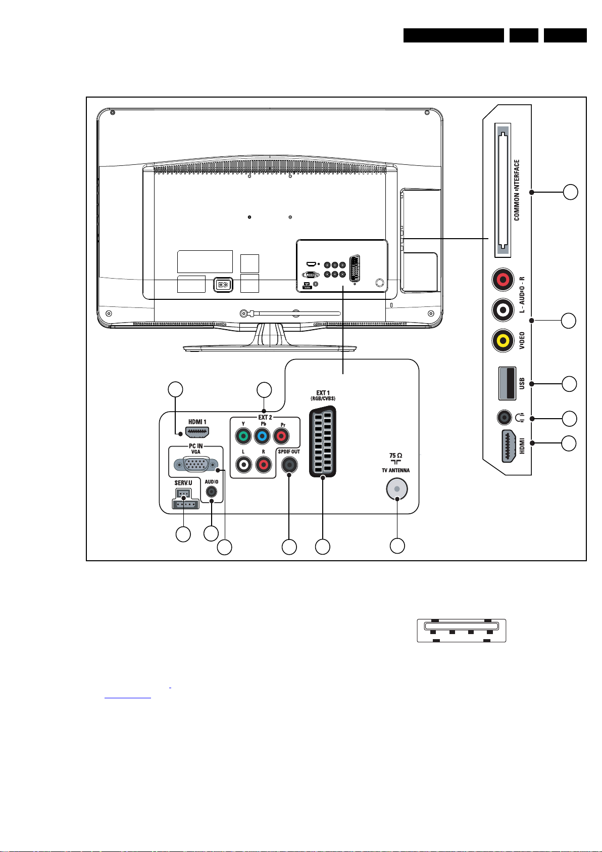
2.3 Connections
1
6
2
3
4
5
7
8
9
11
12
10
13
18840_001_100323.eps
100428
1 2 3 4
10000_022_090121.eps
090121
Technical Specifications, Connections
EN 3TPM5.2E LA 2.
Note: The following connector colour abbreviations are used
(acc. to DIN/IEC 757): Bk= Black, Bu= Blue, Gn= Green,
Gy= Grey, Rd= Red, Wh= White, Ye= Yellow.
2.3.1 Side Connections
1 - Common Interface
68p-See diagram B08
SSB: CI card. jk
2 - Cinch: Audio - In
Ye -Video CVBS 1 V
Rd -Audio R 0.5 V
Wh - Audio L 0.5 V
/ 75 Ω jq
PP
/ 10 kΩ jq
RMS
/ 10 kΩ jq
RMS
Figure 2-1 Connection overview
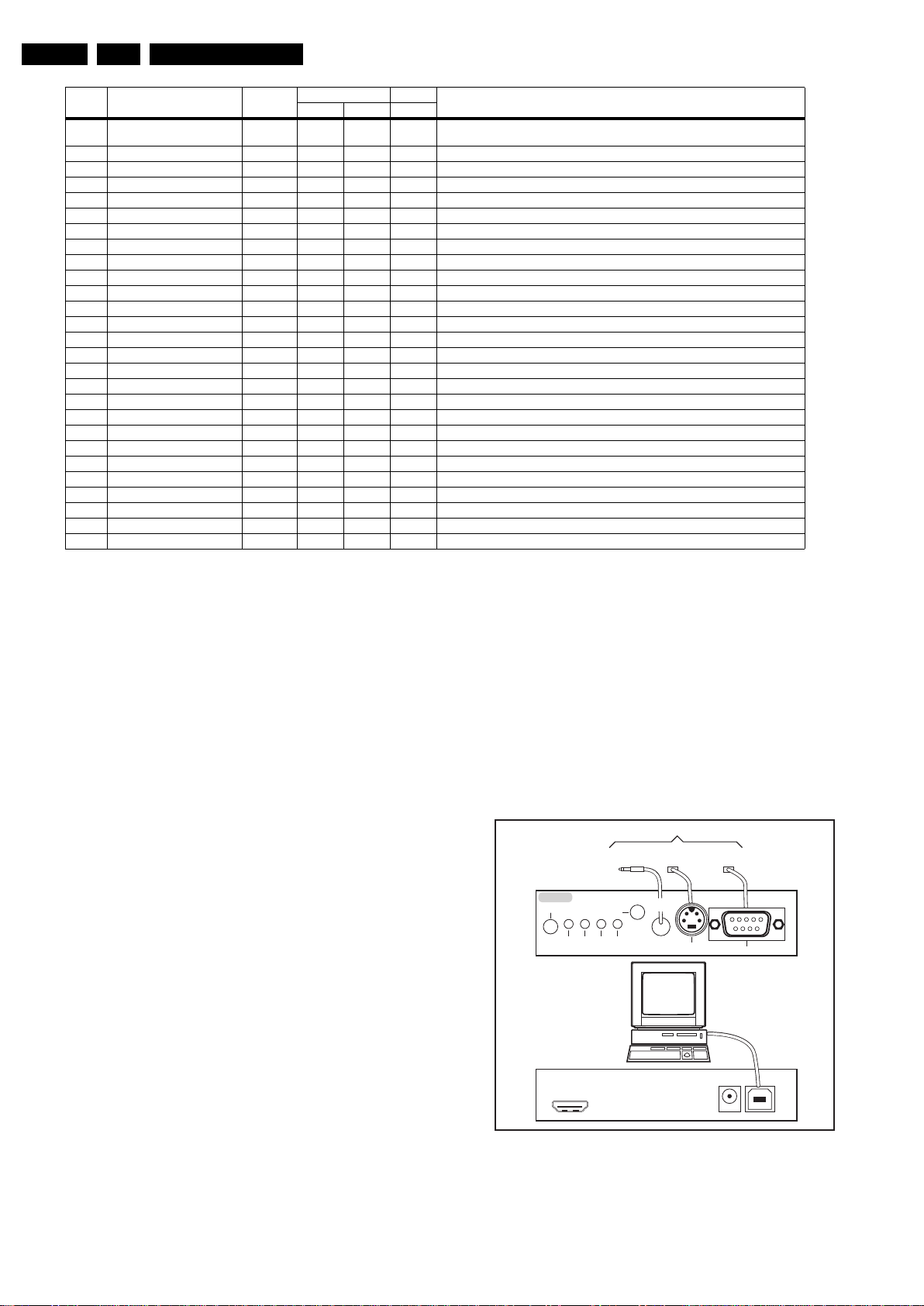
3 - USB2.0
1-+5V k
2 -Data (-) jk
3 -Data (+) jk
4 -Ground Gnd H
4 - Head phone (Output)
Bk -Head phone 80 - 600 Ω / 10 mW ot
Figure 2-2 USB (type A)
2010-Jul-23
Page 4
EN 4 TPM5.2E LA2.
10000_017_090121.eps
090428
19
1
18 2
21
20
1
2
10000_001_090121.eps
090121
1
6
10
11
5
15
10000_002_090121.eps
090127
Technical Specifications, Connections
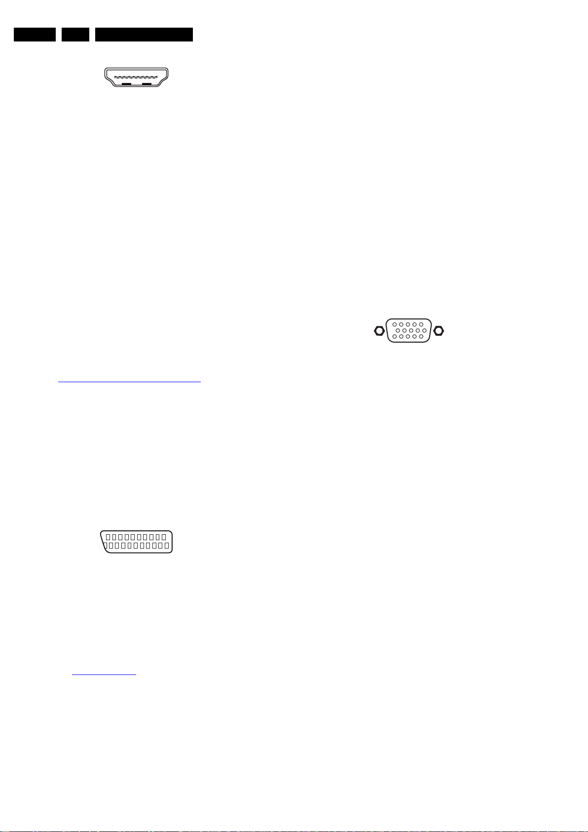
5 - HDMI: Digital Video, Digital Audio - In
Figure 2-3 HDMI (type A) connector
1 -D2+ Data channel j
2 -Shield Gnd H
3 -D2- Data channel j
4 -D1+ Data channel j
5 -Shield Gnd H
6 -D1- Data channel j
7 -D0+ Data channel j
8 -Shield Gnd H
9 -D0- Data channel j
10 - CLK+ Data channel j
11 - Shield Gnd H
12 - CLK- Data channel j
13 - n.c.
14 - n.c.
15 - DDC_SCL DDC clock j
16 - DDC_SDA DDC data jk
17 - Ground Gnd H
18 - +5V j
19 - HPD Hot Plug Detect j
20 - Ground Gnd H
4 -Ground Audio Gnd H
5 -Ground Blue Gnd H
6 -Audio L 0.5 V
7 -Video Blue/C-out 0.7 V
8 -Function Select 0 - 2 V: INT
/ 10 kΩ j
RMS
/ 75 Ω jk
PP
4.5 - 7 V: EXT 16:9
9.5 - 12 V: EXT 4:3 j
9 -Ground Green Gnd H
10 - n.c.
11 - Video Green 0.7 V
12 - n.c.
/ 75 Ω j
PP
13 - Ground Red Gnd H
14 - Ground P50 Gnd H
15 - Video Red/C 0.7 V
/ 75 Ω j
PP
16 - Status/FBL 0 - 0.4 V: INT
1 - 3 V: EXT / 75 Ω j
17 - Ground Video Gnd H
18 - Ground FBL Gnd H
19 - Video CVBS 1 V
20 - Video CVBS/Y 1 V
/ 75 Ω k
PP
/ 75 Ω j
PP
21 - Shield Gnd H
10 - Cinch: S/PDIF - Out
Bk -Coaxial 0.4 - 0.6V
/ 75 ohm kq
PP
11 - PC IN:VGA
2.3.2 Rear Connections
6 - HDMI 1: Digital Video, Digital Audio - In
See 5 - HDMI: Digital Video, Digital Audio - In
7 - EXT2: Video YPbPr - In, Audio - In
Gn - Video - Y 1 V
Bu - Video - Pb 0.7 V
Rd -Video - Pr 0.7 V
Wh - Audio - L 0.5 V
Rd -Audio - R 0.5 V
/ 75 W jq
PP
/ 75 W jq
PP
/ 75 W jq
PP
/ 10 kW jq
RMS
/ 10 kW jq
RMS
8 - TV ANTENNA - In
Signal input from an antenna, cable or satellite.
9 - EXT1: Video RGB/YC - In, CVBS - In/Out, Audio - In/Out
Figure 2-4 SCART connector
1 -Audio R 0.5 V
2 -Audio R 0.5 V
3 -Audio L 0.5 V
/ 1 kΩ k
RMS
/ 10 kΩ j
RMS
/ 1 kΩ k
RMS
.
1 -Video Red 0.7 V
2 -Video Green 0.7 V
3 -Video Blue 0.7 V
4-n.c.
Figure 2-5 VGA connector
/ 75 Ω j
PP
/ 75 Ω j
PP
/ 75 Ω j
PP
5 -Ground Gnd H
6 -Ground Red Gnd H
7 -Ground Green Gnd H
8 -Ground Blue Gnd H
9-+5V
10 - Ground Sync Gnd H
DC
+5 V j
11 - Ground Red Gnd H
12 - DDC_SDA DDC data j
13 - H-sync 0 - 5 V j
14 - V-sync 0 - 5 V j
15 - DDC_SCL DDC clock j
12 - Audio - In: Left / Right, VGA
Gn - Audio L/R in 0.5 V
/ 10 kW jq
RMS
13 - Service / UART
1 -Ground Gnd H
2 -UART_TX Transmit k
3 -UART_RX Receive j
2.4 Chassis Overview
Refer to 9. Block Diagrams for PWB/CBA locations.
2010-Jul-23
Page 5

Precautions, Notes, and Abbreviation List
3. Precautions, Notes, and Abbreviation List
EN 5TPM5.2E LA 3.
Index of this chapter:
3.1 Safety Instructions
3.2 Warnings
3.3 Notes
3.4 Abbreviation List
3.1 Safety Instructions
Safety regulations require the following during a repair:
• Connect the set to the Mains/AC Power via an isolation
transformer (> 800 VA).
• Replace safety components, indicated by the symbol h,
only by components identical to the original ones. Any
other component substitution (other than original type) may
increase risk of fire or electrical shock hazard.
Safety regulations require that after a repair, the set must be
returned in its original condition. Pay in particular attention to
the following points:
• Route the wire trees correctly and fix them with the
mounted cable clamps.
• Check the insulation of the Mains/AC Power lead for
external damage.
• Check the strain relief of the Mains/AC Power cord for
proper function.
• Check the electrical DC resistance between the Mains/AC
Power plug and the secondary side (only for sets that have
a Mains/AC Power isolated power supply):
1. Unplug the Mains/AC Power cord and connect a wire
between the two pins of the Mains/AC Power plug.
2. Set the Mains/AC Power switch to the “on” position
(keep the Mains/AC Power cord unplugged!).
3. Measure the resistance value between the pins of the
Mains/AC Power plug and the metal shielding of the
tuner or the aerial connection on the set. The reading
should be between 4.5 MΩ and 12 MΩ.
4. Switch “off” the set, and remove the wire between the
two pins of the Mains/AC Power plug.
• Check the cabinet for defects, to prevent touching of any
inner parts by the customer.
3.2 Warnings
• All ICs and many other semiconductors are susceptible to
electrostatic discharges (ESD w). Careless handling
during repair can reduce life drastically. Make sure that,
during repair, you are connected with the same potential as
the mass of the set by a wristband with resistance. Keep
components and tools also at this same potential.
• Be careful during measurements in the high voltage
section.
• Never replace modules or other components while the unit
is switched “on”.
• When you align the set, use plastic rather than metal tools.
This will prevent any short circuits and the danger of a
circuit becoming unstable.
3.3 Notes
3.3.1 General
• Measure the voltages and waveforms with regard to the
chassis (= tuner) ground (H), or hot ground (I), depending
on the tested area of circuitry. The voltages and waveforms
shown in the diagrams are indicative. Measure them in the
Service Default Mode with a colour bar signal and stereo
sound (L: 3 kHz, R: 1 kHz unless stated otherwise) and
picture carrier at 475.25 MHz for PAL, or 61.25 MHz for
NTSC (channel 3).
• Where necessary, measure the waveforms and voltages
with (D) and without (E) aerial signal. Measure the
voltages in the power supply section both in normal
operation (G) and in stand-by (F). These values are
indicated by means of the appropriate symbols.
3.3.2 Schematic Notes
• All resistor values are in ohms, and the value multiplier is
often used to indicate the decimal point location (e.g. 2K2
indicates 2.2 kΩ).
• Resistor values with no multiplier may be indicated with
either an “E” or an “R” (e.g. 220E or 220R indicates 220 Ω).
• All capacitor values are given in micro-farads (μ=× 10
nano-farads (n =× 10
• Capacitor values may also use the value multiplier as the
decimal point indication (e.g. 2p2 indicates 2.2 pF).
• An “asterisk” (*) indicates component usage varies. Refer
to the diversity tables for the correct values.
• The correct component values are listed on the Philips
Spare Parts Web Portal.
3.3.3 Spare Parts
For the latest spare part overview, consult your Philips Spare
Part web portal.
3.3.4 BGA (Ball Grid Array) ICs
Introduction
For more information on how to handle BGA devices, visit this
URL: http://www.atyourservice-magazine.com
“Magazine”, then go to “Repair downloads”. Here you will find
Information on how to deal with BGA-ICs.
BGA Temperature Profiles
For BGA-ICs, you must use the correct temperature-profile.
Where applicable and available, this profile is added to the IC
Data Sheet information section in this manual.
3.3.5 Lead-free Soldering
Due to lead-free technology some rules have to be respected
by the workshop during a repair:
• Use only lead-free soldering tin. If lead-free solder paste is
required, please contact the manufacturer of your soldering
equipment. In general, use of solder paste within
workshops should be avoided because paste is not easy to
store and to handle.
• Use only adequate solder tools applicable for lead-free
soldering tin. The solder tool must be able:
– To reach a solder-tip temperature of at least 400°C.
– To stabilize the adjusted temperature at the solder-tip.
– To exchange solder-tips for different applications.
• Adjust your solder tool so that a temperature of around
360°C - 380°C is reached and stabilized at the solder joint.
Heating time of the solder-joint should not exceed ~ 4 sec.
Avoid temperatures above 400°C, otherwise wear-out of
tips will increase drastically and flux-fluid will be destroyed.
To avoid wear-out of tips, switch “off” unused equipment or
reduce heat.
• Mix of lead-free soldering tin/parts with leaded soldering
tin/parts is possible but PHILIPS recommends strongly to
avoid mixed regimes. If this cannot be avoided, carefully
clear the solder-joint from old tin and re-solder with new tin.
3.3.6 Alternative BOM identification
It should be noted that on the European Service website,
“Alternative BOM” is referred to as “Design variant”.
-9
), or pico-farads (p =× 10
. Select
2010-Jul-23
-12
-6
),
).
Page 6
EN 6 TPM5.2E LA3.
Precautions, Notes, and Abbreviation List
The third digit in the serial number (example:
AG2B0335000001) indicates the number of the alternative
B.O.M. (Bill Of Materials) that has been used for producing the
specific TV set. In general, it is possible that the same TV
model on the market is produced with e.g. two different types
of displays, coming from two different suppliers. This will then
result in sets which have the same CTN (Commercial Type
Number; e.g. 28PW9515/12) but which have a different B.O.M.
number.
By looking at the third digit of the serial number, one can
identify which B.O.M. is used for the TV set he is working with.
If the third digit of the serial number contains the number “1”
(example: AG1B033500001), then the TV set has been
manufactured according to B.O.M. number 1. If the third digit is
a “2” (example: AG2B0335000001), then the set has been
produced according to B.O.M. no. 2. This is important for
ordering the correct spare parts!
For the third digit, the numbers 1...9 and the characters A...Z
can be used, so in total: 9 plus 26= 35 different B.O.M.s can be
indicated by the third digit of the serial number.
Identification: The bottom line of a type plate gives a 14-digit
serial number. Digits 1 and 2 refer to the production centre (e.g.
AG is Bruges), digit 3 refers to the B.O.M. code, digit 4 refers
to the Service version change code, digits 5 and 6 refer to the
production year, and digits 7 and 8 refer to production week (in
example below it is 2006 week 17). The 6 last digits contain the
serial number.
MODEL :
PROD.NO:
32PF9968/10
AG 1A0617 000001
MADE IN BELGIUM
220-240V 50/60Hz
VHF+S+H+UHF
S
10000_024_090121.eps
~
BJ3.0E LA
Figure 3-1 Serial number (example)
3.3.7 Board Level Repair (BLR) or Component Level Repair (CLR)
If a board is defective, consult your repair procedure to decide
if the board has to be exchanged or if it should be repaired on
component level.
If your repair procedure says the board should be exchanged
completely, do not solder on the defective board. Otherwise, it
cannot be returned to the O.E.M. supplier for back charging!
3.3.8 Practical Service Precautions
• It makes sense to avoid exposure to electrical shock.
While some sources are expected to have a possible
dangerous impact, others of quite high potential are of
limited current and are sometimes held in less regard.
• Always respect voltages. While some may not be
dangerous in themselves, they can cause unexpected
reactions that are best avoided. Before reaching into a
powered TV set, it is best to test the high voltage insulation.
It is easy to do, and is a good service precaution.
128W
100105
3.4 Abbreviation List
0/6/12 SCART switch control signal on A/V
board. 0 = loop through (AUX to TV),
6 = play 16 :9 format, 12 = play 4: 3
format
AARA Automatic Aspect Ratio Adaptation:
algorithm that adapts aspect ratio to
remove horizontal black bars; keeps
the original aspect ratio
ACI Automatic Channel Installation:
algorithm that installs TV channels
directly from a cable network by
means of a predefined TXT page
ADC Analogue to Digital Converter
AFC Automatic Frequency Control: control
signal used to tune to the correct
frequency
AGC Automatic Gain Control: algorithm that
controls the video input of the feature
box
AM Amplitude Modulation
AP Asia Pacific
AR Aspect Ratio: 4 by 3 or 16 by 9
ASF Auto Screen Fit: algorithm that adapts
aspect ratio to remove horizontal black
bars without discarding video
information
ATSC Advanced Television Systems
Committee, the digital TV standard in
the USA
ATV See Auto TV
Auto TV A hardware and software control
system that measures picture content,
and adapts image parameters in a
dynamic way
AV External Audio Video
AVC Audio Video Controller
AVIP Audio Video Input Processor
B/G Monochrome TV system. Sound
carrier distance is 5.5 MHz
BDS Business Display Solutions (iTV)
BLR Board-Level Repair
BTSC Broadcast Television Standard
Committee. Multiplex FM stereo sound
system, originating from the USA and
used e.g. in LATAM and AP-NTSC
countries
B-TXT Blue TeleteXT
C Centre channel (audio)
CEC Consumer Electronics Control bus:
remote control bus on HDMI
connections
CL Constant Level: audio output to
connect with an external amplifier
CLR Component Level Repair
ComPair Computer aided rePair
CP Connected Planet / Copy Protection
CSM Customer Service Mode
CTI Color Transient Improvement:
manipulates steepness of chroma
transients
CVBS Composite Video Blanking and
Synchronization
DAC Digital to Analogue Converter
DBE Dynamic Bass Enhancement: extra
low frequency amplification
DCM Data Communication Module. Also
referred to as System Card or
Smartcard (for iTV).
DDC See “E-DDC”
D/K Monochrome TV system. Sound
carrier distance is 6.5 MHz
DFI Dynamic Frame Insertion
2010-Jul-23
Page 7

Precautions, Notes, and Abbreviation List
EN 7TPM5.2E LA 3.
DFU Directions For Use: owner's manual
DMR Digital Media Reader: card reader
DMSD Digital Multi Standard Decoding
DNM Digital Natural Motion
DNR Digital Noise Reduction: noise
reduction feature of the set
DRAM Dyna mic RAM
DRM Digital Rights Management
DSP Digital Signal Processing
DST Dealer Service Tool: special remote
control designed for service
technicians
DTCP Digital Transmission Content
Protection; A protocol for protecting
digital audio/video content that is
traversing a high speed serial bus,
such as IEEE-1394
DVB-C Digital Video Broadcast - Cable
DVB-T Digital Video Broadcast - Terrestrial
DVD Digital Versatile Disc
DVI(-d) Digital Visual Interface (d= digital only)
E-DDC Enhanced Display Data Channel
(VESA standard for communication
channel and display). Using E-DDC,
the video source can read the EDID
information form the display.
EDID Extended Display Identification Data
(VESA standard)
EEPROM Electrically Erasable and
Programmable Read Only Memory
EMI Electro Magnetic Interference
EPG Electronic Program Guide
EPLD Erasable Programmable Logic Device
EU Europe
EXT EXTernal (source), entering the set by
SCART or by cinches (jacks)
FDS Full Dual Screen (same as FDW)
FDW Full Dual Window (same as FDS)
FLASH FLASH memory
FM Field Memory or Frequency
Modulation
FPGA Field-Programmable Gate Array
FTV Flat TeleVision
Gb/s Giga bits per second
G-TXT Green TeleteXT
H H_sync to the module
HD High Definition
HDD Hard Disk Drive
HDCP High-bandwidth Digital Content
Protection: A “key” encoded into the
HDMI/DVI signal that prevents video
data piracy. If a source is HDCP coded
and connected via HDMI/DVI without
the proper HDCP decoding, the
picture is put into a “snow vision” mode
or changed to a low resolution. For
normal content distribution the source
and the display device must be
enabled for HDCP “software key”
decoding.
HDMI High Definition Multimedia Interface
HP HeadPhone
I Monochrome TV system. Sound
2
C Inter IC bus
I
2
D Inter IC Data bus
I
2
S Inter IC Sound bus
I
carrier distance is 6.0 MHz
IF Intermediate Frequency
IR Infra Red
IRQ Interrupt Request
ITU-656 The ITU Radio communication Sector
(ITU-R) is a standards body
subcommittee of the International
Telecommunication Union relating to
radio communication. ITU-656 (a.k.a.
SDI), is a digitized video format used
for broadcast grade video.
Uncompressed digital component or
digital composite signals can be used.
The SDI signal is self-synchronizing,
uses 8 bit or 10 bit data words, and has
a maximum data rate of 270 Mbit/s,
with a minimum bandwidth of 135
MHz.
ITV Institutional TeleVision; TV sets for
hotels, hospitals etc.
LS Last Status; The settings last chosen
by the customer and read and stored
in RAM or in the NVM. They are called
at start-up of the set to configure it
according to the customer's
preferences
LATAM Latin America
LCD Liquid Crystal Display
LED Light Emitting D iode
L/L' Monochrome TV system. Sound
carrier distance is 6.5 MHz. L' is Band
I, L is all bands except for Band I
LPL LG.Philips LCD (supplier)
LS Loudspeaker
LVDS Low Voltage Differential Signalling
Mbps Mega bits per second
M/N Monochrome TV system. Sound
carrier distance is 4.5 MHz
MHEG Part of a set of international standards
related to the presentation of
multimedia information, standardised
by the Multimedia and Hypermedia
Experts Group. It is commonly used as
a language to describe interactive
television services
MIPS Microprocessor without Interlocked
Pipeline-Stages; A RISC-based
microprocessor
MOP Matrix Output Processor
MOSFET Metal Oxide Silicon Field Effect
Transistor, switching device
MPEG Motion Pictures Experts Group
MPIF Multi Platform InterFace
MUTE MUTE Line
MTV Mainstream TV: TV-mode with
Consumer TV features enabled (iTV)
NC Not Connected
NICAM Near Instantaneous Compounded
Audio Multiplexing. This is a digital
sound system, mainly used in Europe.
NTC Negative Temperature Coefficient,
non-linear resistor
NTSC National Television Standard
Committee. Color system mainly used
in North America and Japan. Color
carrier NTSC M/N= 3.579545 MHz,
NTSC 4.43= 4.433619 MHz (this is a
VCR norm, it is not transmitted off-air)
NVM Non-Volatile Memory: IC containing
TV related data such as alignments
O/C Open Circuit
OSD On Screen Display
OAD Over the Air Download. Method of
software upgrade via RF transmission.
Upgrade software is broadcasted in
TS with TV channels.
OTC On screen display Teletext and
Control; also called Artistic (SAA5800)
P50 Project 50: communication protocol
between TV and peripherals
PAL Phase Alternating Line. Color system
mainly used in West Europe (color
carrier= 4.433619 MHz) and South
America (color carrier PAL M=
2010-Jul-23
Page 8

EN 8 TPM5.2E LA3.
Precautions, Notes, and Abbreviation List
3.575612 MHz and PAL N= 3.582056
MHz)
PCB Printed Circuit Board (same as “PWB”)
PCM Pulse Code Modulation
PDP Plasma Display Panel
PFC Power Factor Corrector (or Pre-
conditioner)
PIP Picture In Picture
PLL Phase Locked Loop. Used for e.g.
FST tuning systems. The customer
can give directly the desired frequency
POD Point Of Deployment: a removable
CAM module, implementing the CA
system for a host (e.g. a TV-set)
POR Power On Reset, signal to reset the uP
PSDL Power Supply for Direct view LED
backlight with 2D-dimming
PSL Power Supply with integrated LED
drivers
PSLS Power Supply with integrated LED
drivers with added Scanning
functionality
PTC Positive Temperature Coefficient,
non-linear resistor
PWB Printed Wiring Board (same as “PCB”)
PWM Pulse Width Modulation
QRC Quasi Resonant Converter
QTNR Quality Temporal Noise Reduction
QVCP Quality Video Composition Processor
RAM Random Access Memory
RGB Red, Green, and Blue. The primary
color signals for TV. By mixing levels
of R, G, and B, all colors (Y/C) are
reproduced.
RC Remote Control
RC5 / RC6 Signal protocol from the remote
control receiver
RESET RESET signal
ROM Read Only Memory
RSDS Reduced Swing Differential Signalling
data interface
R-TXT Red TeleteXT
SAM Service Alignment Mode
S/C Short Circuit
SCART Syndicat des Constructeurs
d'Appareils Radiorécepteurs et
Téléviseurs
SCL Serial Clock I
SCL-F CLock Signal on Fast I
SD Standard Definition
SDA Serial Data I
SDA-F DAta Signal on Fast I
2
C
2
C bus
2
C
2
C bus
SDI Serial Digital Interface, see “ITU-656”
SDRAM Synchronous DRAM
SECAM SEequence Couleur Avec Mémoire.
Color system mainly used in France
and East Europe. Color carriers=
4.406250 MHz and 4.250000 MHz
SIF Sound Intermediate Frequency
SMPS Switched Mode Power Supply
SoC System on Chip
SOG Sync On Green
SOPS Self Oscillating Power Supply
SPI Serial Peripheral Interface bus; a 4-
wire synchronous serial data link
standard
S/PDIF Sony Philips Digital InterFace
SRAM Static RAM
SRP Service Reference Protocol
SSB Small Signal Board
SSC Spread Spectrum Clocking, used to
reduce the effects of EMI
STB Set Top Box
STBY STand-BY
SVGA 800 × 600 (4:3)
SVHS Super Video Home System
SW Software
SWAN Spatial temporal Weighted Averaging
Noise reduction
SXGA 1280 × 1024
TFT Thin Film Transistor
THD Total Harmonic Distortion
TMDS Transmission Minimized Differential
Signalling
TS Transport Stream
TXT TeleteXT
TXT-DW Dual Window with TeleteXT
UI User Interface
uP Microprocessor
UXGA 1600 × 1200 (4:3)
V V-sync to the module
VESA Video Electronics Standards
Association
VGA 640 ×480 (4:3)
VL Variable Level out: processed audio
output toward external amplifier
VSB Vestigial Side Band; modulation
method
WYSIWYR What You See Is What You Record:
record selection that follows main
picture and sound
WXGA 1280 ×768 (15:9)
XTAL Quartz crystal
XGA 1024 × 768 (4:3)
Y Luminance signal
Y/C Luminance (Y) and Chrominance (C)
signal
YPbPr Component video. Luminance and
scaled color difference signals (B-Y
and R-Y)
YUV Component video
2010-Jul-23
Page 9

4. Mechanical Instructions
18840_101_100324.eps
100324
Mechanical Instructions
EN 9TPM5.2E LA 4.
Index of this chapter:
4.1 Cable Dressing
4.2 Service Positions
4.3 Assembly/Panel Removal
4.4 Set Re-assembly.
4.1 Cable Dressing
Notes:
• Figures below can deviate slightly from the actual situation,
due to the different set executions.
Figure 4-1 Cable dressing (19")
2010-Jul-23
Page 10

EN 10 TPM5.2E LA4.
18840_102_100324.eps
100324
Mechanical Instructions
Figure 4-2 Cable dressing (22")
2010-Jul-23
Page 11
Mechanical Instructions
18840_104_100324.eps
100324
18840_106_100422.eps
100422
3
1
1
1
1
2
EN 11TPM5.2E LA 4.
Figure 4-3 Cable dressing (26")
4.2 Service Positions
For easy servicing of a TV set, the set should be put face down
on a soft flat surface, foam buffers or other specific workshop
tools. Ensure that a stable situation is created to perform
measurements and alignments. When using foam bars take
care that these always support the cabinet and never only the
display. Caution: Failure to follow these guidelines can
seriously damage the display!
Ensure that ESD safe measures are taken.
4.3 Assembly/Panel Removal
Instructions below apply to the 19PFL3405H/xx, but are similar
for other models.
4.3.1 Rear Cover
Warning: Disconnect the mains power cord before removing
the rear cover.
1. Remove the fixation screws that secure the stand at the
bottom of the stand. Then remove the stand.
2. Remove fixation screws [1], [2] and [3] that secure the rear
cover, see Figure 4-4
3. The rear cover is secured with locking clips at the side and
top of the cabinet. Pull the rear cover from the TV. This may
require more than average force. Be sure to oppose to
the stand support. Make sure that wires and flat foils are
not damaged while lifting the rear cover from the set, see
Figure 4-5
and Figure 4-6.
.
Figure 4-4 Rear cover removal [1/3]
2010-Jul-23
Page 12

EN 12 TPM5.2E LA4.
18840_107_100422.eps
100422
Pull up
18840_103_100324.eps
100429
1
Figure 4-5 Rear cover removal [2/3]
Mechanical Instructions
4.3.4 Speakers
1. Release the speaker cable from its clamps.
2. Unplug the speaker connector from the SSB.
3. Take the speakers out.
When defective, replace the whole unit.
4.3.5 Stand removal
Caution: it is mandatory to remount all different screws at their
original position during re-assembly. Be sure to put the set in
the Service Position.
1. Remove the speaker cables as described earlier.
2. Remove the fixation screws.
3. Take the stand out.
4.3.6 IR/LED Board
4. Unplug the connectors from the IR/LED board.
5. Remove the fixation screw.
6. Release the clips that hold the board and take it out from
the bezel.
When defective, replace the whole unit.
4.3.7 Keyboard Control Panel
Pull up
18840_108_100422.eps
Figure 4-6 Rear cover removal [3/3]
4.3.2 Small Signal Board (SSB)
Caution: it is mandatory to remount all different screws at their
original position during re-assembly. Failure to do so may result
in damaging the SSB.
1. Release the Connector from the Flat Foil connectors.
Caution: be careful, as these are very fragile connectors!
Take the flat foils out of their connectors.
2. Unplug all other connectors.
3. Remove the fixation screw near the L-R audio side inputs.
4. Remove all other fixation screws from the SSB.
5. Take the SSB out.
100422
Refer to Figure 4-7
.
1. Unplug the connector [1] on the IR/LED board that leads to
the Local Control board, as it is not unplug-able at the Local
Control board itself (soldered connector).
2. Release the cable from its tape.
3. Put your thumbs against the front bezel while pulling the
Local Control board in the direction of the arrow .
When defective, replace the whole unit.
4.3.3 Power Supply Unit (PSU)
Caution: it is mandatory to remount all different screws at their
original position during re-assembly. Failure to do so may result
in damaging the PSU.
1. Release the Power board cables from their clamps.
2. Unplug power connector from the SSB and LCD panel.
3. Remove all fixation screws from the PSU.
4. The PSU can now be taken out of the set.
When defective, replace the whole unit.
2010-Jul-23
Figure 4-7 Keyboard Control Panel
Page 13

4.3.8 LCD Panel
1. Remove the SSB as described earlier.
2. Remove the PSU as described earlier.
3. Remove the speaker as described earlier.
4. Remove the stand as described earlier.
5. Release the tape that fix the Keyboard Control cable near
the Keyboard Control panel.
6. Remove the fixation screws that secure the LCD panel with
the bezel.
7. Lift the LCD Panel from the bezel.
8. Remove the fixation screws that secure the panel with the
Metal frame.
9. Take the panel out. Remove the Flat Foil connector from
the panel.
When defective, replace the whole unit.
4.4 Set Re-assembly
To re-assemble the whole set, execute all processes in reverse
order.
Notes:
• While re-assembling, make sure that all cables are placed
and connected in their original position. See Figure 4-1
and Figure 4-2
• Pay special attention not to damage the EMC foams on the
SSB shields. Ensure that EMC foams are mounted
correctly.
.
Mechanical Instructions
EN 13TPM5.2E LA 4.
2010-Jul-23
Page 14

EN 14 TPM5.2E LA5.
18840_200_100324.eps
100324
18840_202_100324.eps
100428
Service Modes, Error Codes, and Fault Finding
5. Service Modes, Error Codes, and Fault Finding
Index of this chapter:
5.1 Service Modes
5.2 Service Tools
5.3 Software Upgrading
5.4 Error Codes
5.5 Fault Finding and Repair Tips
5.1 Service Modes
The Customer Service Mode (CSM) is used for communication
between the call centre and the customer, while the Service
Alignment Mode (SAM) offers several features for the service
technician.
This chassis also offers the option of using ComPair, a
hardware interface between a computer and the TV chassis. It
offers the abilities of structured troubleshooting, error code
reading, and software version read-out for all chassis.
5.1.1 Customer Service Mode (CSM)
How to Navigate
By means of the “CURSOR-DOWN/UP” knob (or the scroll
wheel) on the RC-transmitter, can be navigated through the
menus.
Figure 5-3 CSM Menu 3
Purpose
The Customer Service Mode shows error codes and
information on the TV's operation settings.The call centre can
instruct the customer (by telephone) to enter CSM in order to
identify the status of the set.This helps the call centre to
diagnose problems and failures in the TV set before making a
service call.
The CSM is a read-only mode; therefore, modifications are not
possible in this mode.
How to Activate CSM
Key in the code “123654” via the standard RC transmitter.
Note: Activation of the CSM is only possible if there is no (user)
menu on the screen!
Figure 5-1 CSM Menu 1
General
• 1.1 Set Type NVM read/write (max. 16 characters).
• 1.2 Production code NVM read/write (max. 16
characters).
• 1.3 Installation date Date the software was installed.
• 1.4 Option Code Store in NVM (set feature grouping as
option) panel code.
• 1.5 Codes Error code Layer 2. Store in NVM. 10 error
buffers: 000 = No problem, 011 = I
2
C bus error,
012 = tuner error, 013 = panel.
• 1.6 SSB 12NC NVM read/write (12 characters).
• 1.7 Display 12NC NVM read/write (12 characters).
• 1.8 PSU 12NC NVM read/write (12 characters).
• 2.1 Current Main SW Detects and displays software
version.
• 2.2 Stand-by SW Detects and displays software version.
• 2.3 SW version of other μP Detects and displays software
version.
• 2.4 Reserved Not applicable.
• 2.5 Reserved Not applicable.
• 2.6 NVM version Detects and displays software version.
• 3.1 Signal Quality/Present analog/digital signal strength.
• 3.2 Child lock Detects and displays.
• 3.3 HDCP keys Detects and displays.
• 3.4 CI slot present Detects and displays.
• 3.5 HDMI input format per Supported format. e.g.
576i 50 Hz, 576p 50 Hz, 720p50 Hz, 1080i 50 Hz,
1080p50Hz.
• 3.6 HDMI audio format input stream Per supported
format e.g. Dolby TrueHD, DTS-HD Master Audio, MPCM.
• 3.7 HDMI video format input stream Per Supported
format. e.g. 576i 50 Hz, 576p 50 Hz, 720p50 Hz,
1080i 50 Hz, 1080p 50 Hz
2010-Jul-23
Figure 5-2 CSM Menu 2
18840_201_100324.eps
100429
How to Exit CSM
Press “MENU” on the RC-transmitter.
Page 15
Service Modes, Error Codes, and Fault Finding
18840_203_100324.eps
100324
18840_207_100422.eps
100422
EN 15TPM5.2E LA 5.
5.1.2 Service Alignment Mode (SAM)
How to enter
To enter the factory mode, use the following method:
• Press the following key sequence on the remote control
transmitter: “062596” directly followed by the “INFO”
button.
After entering the factory mode, the following screen is visible
on the top and right of the panel.
Figure 5-4 Example of SAM - 1 -
Table 5-1 Contents of SAM
Number Action Items Range Default Value Description
0 F/W Version
1 Panel_ID 119 120 121 panel identification
2Err Code:000000000000000 ---Show the latest 5 error code status
3 Clear Error Buffer Press OK Press OK Press OK Reset CSM ERROR Code to 0
4NVM Address 000The address in the NVM
5NVM Value 111The value in the NVM
6 NVM Store Press OK Press OK Press OK Store in the NVM
7 NVM Copy TV to USB Press OK Press OK Press OK Use this to copy the NVM data from the TV to the USB
8 NVM Read USB to TV Press OK Press OK Press OK Use this to copy the NVM data from the USB to the TV
9 CLR_Temp_R 0 - 255 119 128 126 Back-End Scaler R G B Gain NVM has for YPbPr four settings: NORMAL, WA RM, COOL,
10 CLR_Temp_G 0 - 255 128 128 128
11 CLR_Temp_B 0 - 255 116 80 100
12 Auto_Color Press OK Press OK Press OK
13 ADC_Gain_R 0 - 255 79 0 85 Analogue to Digital Converter Gain for R ed, AutoColor affe cts this and it va lue is depends
14 ADC_Gain_G 0 - 255 78 0 87 Analogue to Digital Converter Gain for Green, AutoColor affects this and it value is de-
15 ADC_Gain_B 0 - 255 79 0 87 Analogue to Digital Converter Gain for Blue, AutoColor affects this and it value is depends
16 ADC_Offset_R 0 - 255 113 128 113
17 ADC_Offset_G 0 - 255 109 128 109
18 ADC_Offset_B 0 - 255 100 128 100
19 Virgin_Mode Off Off Off Reset the set to manufacturer's mode
20 Gamma_Table On On On use gamma table or not
21 E-Fuse On On On use efuse as default ADC value or not
22 Ageing Mode Off Off Off turn on ageing mode
23 Reset_PBS_PWD Press OK Press OK Press OK Clear NVM EEP_OFFSET_BDS_PCODE_1_4, EEP_OFFSET_BDS_PCODE_2_4,
24 V-COM Press OK Press OK Press OK This starts V-COM
25 Video_PWM_Medium 0 - 255 128 128 128 PWM value at contrast 50%
26 Video_PWM_Minmum 0 - 255 240 240 240 Minimum PWM value
27Video_PWM_Maximun 0 - 255000Maximum PWM value
28 Video_PWM_Ratio_Top 0 - 100 90 90 90 PWM value at Best Power
29Video_PWM_Ratio_Bottom0 - 100555PWM value at Best Picture
30 Video_PWM_Ratio_STD 0 - 100 95 95 95 PWM value at standard
31 YPBPR_PHASE 0 - 255 InValid InValid InValid 480i, 480p, 576i, 576p, 720p 50 Hz, 720p 60 Hz,1080i 25 Hz,1080i 30 Hz,
32 AUD_GAIN_LINEIN 0 - 36 29 29 22 Audio gain by different sources
33 AUD_GAIN_HDMI 0 - 36 29 29 22 Audio gain for HDMI inputs
34 AUD_GAIN_ATV 0 - 36 29 29 22 Audio gain for analogue TV signals
35 AUD_GAIN_DTV 0 - 36 29 29 22 Audio gain for digital TV signal
36 AUD_GAIN_USB 0 - 36 29 29 22 Audio gain for the USB input
37 AUD_LIPSYNC_SPK -272 - +272 200 200 200 Audio delay to the speaker, “+” is delay, “-” is ahead. NVM value = Delay(ms)/0.147
38 AUD_LIPSYNC_HP -272 - +272 200 200 200 Audio delay to the head-phone, “+” is del ay, “- ” is a head. NVM value = Delay(ms)/0.147
Press OK Press OK Press OK
19" 22" 26"
Press “OK” to check the Version information of the software
when you select the “0. F/W Version”.
Figure 5-5 Example of SAM - 2 -
Version description
CUSTOMER. Other source use offset with hardcoding.
PC: any pattern has black and white YPbPr: SMPTE bar (colour bar), any timing.
on the input
pends on the input
on the input
Analogue to Digital Converter Offset for Red, AutoColor affects this and it value is de-
pends on the input
Analogue to Digital Converter Offset for Green, AutoColor affects this and it value is de-
pends on the input
Analogue to Digital Converter Offset for Blue, AutoColor affects this and it value is de-
pends on the input
EEP_OFFSET_BDS_PCODE_3_4, EEP_OFFSET_BDS_PCODE_4_4
1080p 24 Hz,1080p 50 Hz,1080p 60 Hz
2010-Jul-23
Page 16
EN 16 TPM5.2E LA5.
10000_036_090121.eps
091118
TO
UART SERVICE
CONNECTOR
TO
UART SERVICE
CONNECTOR
TO
I2C SERVICE
CONNECTOR
TO TV
PC
HDMI
I
2
C only
Optional power
5V DC
ComPair II Developed by Philips Brugge
RC out
RC in
Optional
Switch
Power ModeLink/
Activity
I
2
C
ComPair II
Multi
function
RS232 /UART
Number Action Items Range Default Value Description
39 AUD_LIPSYNC_SPDIF -272 - +272 200 200 200 Audio delay to the S/P-DIF output, “+” is delay, “-” is ahead. NVM value = Delay(ms)/
40 Tuner_ID 95 95 95 Tuner Identification, 94: NXP 95: LG
41OPT AV2 Scart2 0, 20000: not available, 2: CVBS + YC
42OPT HDMI2 0/1001On/Off
43 OPT Reset Option 0/1 Press OK Press OK Press OK after reset, should restart the set immediately
44 Esticker NVM 1 0 - 61, 255 32 32 32 0~61: Icon number. 255: no icon
45 Esticker NVM 2 0 - 61, 255 79 79 79 0~61: Icon number. 255: no icon
46 Esticker NVM 3 0 - 61, 255 77 77 83 0~61: Icon number. 255: no icon
47 Esticker NVM 4 0 - 61, 255 35 35 85 0~61: Icon number. 255: no icon
48 Esticker NVM 5 0 - 61, 255 7 7 45 0~61: Icon number. 255: no icon
49 Esticker NVM 6 0 - 61, 255 45 45 2 0~61: Icon number. 255: no icon
50 Esticker NVM 7 0 - 61, 255 0 0 58 0~61: Icon number. 255: no icon
51 Esticker NVM 8 0 - 61, 255 58 58 48 0~61: Icon number. 255: no icon
52 Esticker NVM 9 0 - 61, 255 48 48 81 0~61: Icon number. 255: no icon
53 Esticker NVM 10 0 - 61, 255 64 64 64 0~61: Icon number. 255: no icon
54 Esticker NVM 11 0 - 61, 255 77 77 86 0~61: Icon number. 255: no icon
55 Esticker NVM 12 0 - 61, 255 76 76 76 0~61: Icon number. 255: no icon
56 Esticker NVM 13 0 - 61, 255 71 71 71 0~61: Icon number. 255: no icon
57 Esticker NVM 14 0 - 61, 255 70 70 70 0~61: Icon number. 255: no icon
58 Esticker NVM 15 0 - 61, 255 74 74 74 0~61: Icon number. 255: no icon
59 Esticker NVM 16 0 - 61, 255 72 72 72 0~61: Icon number. 255: no icon
60 Esticker NVM 17 0 - 61, 255 78 78 78 0~61: Icon number. 255: no icon
61 Esticker NVM 18 0 - 61, 255 255 255 255 0~61: Icon number. 255: no icon
62 Esticker NVM 19 0 - 61, 255 255 255 255 0~61: Icon number. 255: no icon
63 Esticker NVM 20 0 - 61, 255 255 255 255 0~61: Icon number. 255: no icon
64 Esticker Reset Press OK Press OK Press OK Executing this resets the e-sticker
65 Exit_Factory Press OK Press OK Press OK Exit factory mode
Service Modes, Error Codes, and Fault Finding
19" 22" 26"
0.147
How to Navigate
With the up/down cursor keys can be used to navigate through
the menu, while with the Left/Right cursor the values can be
changed.
How to EXIT
Choose “EXIT”, and press the “OK” button. Turn “Off” the TV
via the side control key and then turn “On” the TV again.
5.1.3 Hotel mode
Notes: (only applicable to xxHFLxxxxX/nn)
• Refer to the user manual for more information on the hotel
mode.
• When in the hotel mode, the service modes CSM, SDM,
SAM and ComPair are automatically disabled (this is to
prevent hotel guests entering Philips service modes).
• In order to use the service modes and ComPair, hotel
mode must be disabled.
• To enable/disable the hotel mode, the hotel setup remote
(green remote) is needed.
5.2 Service Tools
5.2.1 ComPair
Introduction
ComPair (Computer Aided Repair) is a Service tool for Philips
Consumer Electronics products. and offers the following:
1. ComPair helps to quickly get an understanding on how to
repair the chassis in a short and effective way.
2. ComPair allows very detailed diagnostics and is therefore
capable of accurately indicating problem areas. No
knowledge on I
because ComPair takes care of this.
3. ComPair speeds up the repair time since it can
automatically communicate with the chassis (when the uP
is working) and all repair information is directly available.
4. ComPair features TV software upgrade possibilities.
2010-Jul-23
2
C or UART commands is necessary,
Specifications
ComPair consists of a Windows based fault finding program
and an interface box between PC and the (defective) product.
The ComPair II interface box is connected to the PC via an
USB cable. For the TV chassis, the ComPair interface box and
the TV communicate via a bi-directional cable via the service
connector(s).
The ComPair fault finding program is able to determine the
problem of the defective television, by a combination of
automatic diagnostics and an interactive question/answer
procedure.
How to Connect
This is described in the chassis fault finding database in
ComPair.
Figure 5-6 ComPair II interface connection
Caution: It is compulsory to connect the TV to the PC as
shown in the picture above (with the ComPair interface in
between), as the ComPair interface acts as a level shifter. If
Page 17

Service Modes, Error Codes, and Fault Finding
18850_204_100204.eps
100204
18850_205_100204.eps
100204
18850_206_100204.eps
100204
one connects the TV directly to the PC (via UART), ICs will be
damaged!
How to Order
ComPair II order codes:
• ComPair II interface: 3122 785 90630.
• Programming software can be downloaded from the Philips
Service portal.
• ComPair UART interface cable for TPM5.2x xx.
3122 785 90630.
Note: While having problems, contact the local support desk.
5.3 Software Upgrading
5.3.1 Introduction
Philips continuously tries to improve its products, and we
recommend that you update the TV software when updates are
available. Software update files can be obtained from your
dealer or can be downloaded from the following websites:
http://www.philips.com/support
Preparing a portable memory for software upgrade
You require the following:
1. A personal computer connected to the Internet.
2. An archive utility that supports the ZIP-format (e.g. WinZip
for Windows or Stufflt for Mac OS).
3. A USB flash drive (preferably empty).
EN 17TPM5.2E LA 5.
Figure 5-7 Update the TV software 1
Note:
1. Only FAT/DOS-formatted flash drives are supported.
2. Only use software update files that can be found on the
http://www.philips.com/support
web site.
5.3.2 Check the current TV software version
Before starting the software upgrade procedure, it is advised to
check that what the current TV software:
1. Press the “Menu” button on your remote control.
2. Select “Setup” and press “OK”, then select [Software
update] > [Current software].
If the current software version of your TV is the same as the
latest update file found on http://www.philips.com/support
not necessary to update the TV software.
5.3.3 Download the latest software
1. Point your web browser to http://www.philips.com/support
2. Find information and software related to your TV.
3. Select the latest software update file and download it to
your PC.
4. Insert a USB flash drive into one of the USB ports of your
PC.
5. Decompress the downloaded ZIP file and copy the
“autorun.upg” to the root directory of the USB flash drive.
5.3.4 Update the TV software
1. Insert the USB flash drive that contains the software
update file.
2. Then a window jumps out as Figure 5-7
.
Note: If the USB flash drive is not detected after power up,
disconnect it and re-insert it.
3. Select [Update] and press OK.
4. To proceed, In next menu select [Start] and press OK to
start software updates. See Figure 5-8
.
5. Upgrading will now begins and the status of the updating
progress will be displayed.
6. When the TV software is updated. Remove your USB flash
drive, then select [Restart] and press OK to restart the
TV.See Figure 5-9
.
Figure 5-8 Update the TV software 2
, it is
.
Figure 5-9 Update the TV software 3
Note:
• Do not remove the USB flash drive during the software
update.
• If a power failure occurs during the update, do not remove
the USB flash drive from the TV. The TV will continue the
software update as soon as power comes back.
• If an error occurs during the update retry the procedure or
contact your dealer.
• We do not recommend downgrading to an older version.
• Once the upgrade is finished, use your PC to remove the
TV software from your USB portable memory.
2010-Jul-23
Page 18

EN 18 TPM5.2E LA5.
5.4 Error Codes
The error code buffer contains all errors detected since the last
time the buffer was erased. The buffer is written from left to
right. When an error occurs that is not yet in the error code
buffer, it is displayed at the left side and all other errors shift one
position to the right.
Basically there are three kinds of error codes:
Error Code Event
000 No problem
011 I
012 Tuner error
013 panel
2
C bus error
5.5 Fault Finding and Repair Tips
5.5.1 Speakers
Make sure that the volume is set to minimum during
disconnecting the speakers in the ON-state of the TV. The
audio amplifier can be damaged by disconnecting the speakers
during ON-state of the set!
Service Modes, Error Codes, and Fault Finding
5.5.2 Tuner
Attention: In case the tuner is replaced, always check the tuner
options.
2010-Jul-23
Page 19

6. Alignments
Alignments
EN 19TPM5.2E LA 6.
Index of this chapter:
6.1 General Alignment Conditions
6.2 Hardware Alignments
6.3 YPbPr Mode display adjustment
6.4 PC mode display adjustment
6.5 Option Settings
Note: The Service Alignment Mode (SAM) are described in
chapter 5. Service Modes, Error Codes, and Fault Finding
Menu navigation is done with the CURSOR UP, DOWN, LEFT
or RIGHT keys of the remote control transmitter.
6.1 General Alignment Conditions
Perform all electrical adjustments under the following
conditions:
• Power supply voltage: 195 - 264 V
• Connect the set to the mains via an isolation transformer
with low internal resistance.
• Allow the set to warm up for approximately 15 minutes.
• Measure voltages and waveforms in relation to correct
ground.
Caution: It is not allowed to use heatsinks as ground.
• Test probe: R
• Use an isolated trimmer/screwdriver to perform
alignments.
> 10 MΩ, Ci < 20 pF.
i
, 50/ 60 ± 3 Hz.
AC
6.2 Hardware Alignments
ADC_GAIN_B and ADC_OFFSET_R, ADC_OFFSET_G,
ADC_OFFSET_B. Then store those values to NVM.
2. Apply 100% white pattern.
3. Set colour temperature to “NORMAL”.
4. At FAC mode menu, adjust the CLR TEMP R, CLR TEMP
G, CLR TEMP B values to meet “NORMAL” colour
coordinates specification below. Then store those values to
NVM (R/G/B gain value ≤128).
.
5. Set colour temperature to “COOL”.
6. At FAC mode menu, adjust the CLR TEMP R, CLR TEMP
G, CLR TEMP B values to meet “COOL” colour
coordinates specification below. Then store those values to
NVM (R/G/B gain value ≤128).
7. Set colour temperature to “WARM”.
8. At FAC mode menu, adjust the CLR TEMP R, CLR TEMP
G, CLR TEMP B values to meet “WARM” colour
coordinates specification below. Then store those values to
NVM (R/G/B gain value ≤128).
Colour temperature Normal/Warm/Cool (x, y) co-ordinates
specification:
Table 6-1 Reading with Minolta CS-200
Picture Mode x y
Normal (9000K) 0.287 ±0.003 0.296 ±0.003
Cool (11000K) 0.276 ±0.003 0.282 ±0.003
Warm (6500K) 0.313 ±0.003 0.329 ±0.003
Not applicable.
6.3 YPbPr Mode display adjustment
6.3.1 General set-up
Equipment Requirements:
Minolta CS-200 or equivalent Colour analyser, Quantum Data
Pattern Generator 802G, 802BT or equivalent instrument.
Input requirements:
Input Signal Type: YPbPr signal
• 1080i mode, TVBar100 pattern by 802G or 802BT.
• Select Picture mode to User mode and check the x, y data.
Input Signal Strength:
for Y signal; 700 mVpp for Pb & Pr signal
1 V
pp
Input Injection Point:
YPbPr (RAC jack)
6.3.2 Alignment method
Quantum Data Pattern Generator 802G or 802BT. Apply 1080i,
and the pattern TVBAR100 with a Quantum colour analyser.
Initial Set-up:
1. Select source as “EXT2”.
2. Set Smart Picture mode as “Standard” and off the
“Dynamic contrast/Dynamic backlight”.
3. Apply “TVBar100” pattern with colour bar pattern by signal
generator.
4. Enter factory mode menu: press numeric keys
“062596” + INFO key (FAC mode menu).
Alignment:
1. At SAM mode menu, select AUTO_COLOR item. Then
press “OK” key to adjust ADC_GAIN_R, ADC_GAIN_G,
If you have not such equipment, the below value is for your
reference.
Table 6-2 Reference value
Colour temperature
Picture Mode Size
Normal (9000K) 19" 128 128 107
22" 116 128 111
26" 126 128 100
Cool (11000K) 19" 119 128 116
22" 105 128 124
26" 111 128 120
Warm (6500K) 19" 128 116 70
22" 128 128 80
26" 128 109 56
Note:
• Check Luminance:
Use Minolta CS-200 or equivalent colour analyser for
colour coordinates and luminance check. Then locate the
colour analyser receiver at the centre of the screen.
When Brightness/Contrast/Video Contrast setting at 100
and CLR_TEMP_R/CLR_TEMP_G/CLR_TEMP_B =128.
The luminance needs to be greater than 240 cd/m
and 22" sets and greater than 320 cd/m
• An equivalent colour analyser needs to be calibrated to
deliver similar measurements as the Minolta CS-200.
Red Green Blue
6.4 PC mode display adjustment
6.4.1 Display quality adjustment
Use the POPO (pixel on pixel off) pattern to adjust the clock
until no stripe and adjust the phase until clear picture (“Auto”
will be done every time switching to PC mode and mode
change).
2
for 26".
2
for 19"
2010-Jul-23
Page 20

EN 20 TPM5.2E LA6.
18290_201_090330.eps
090416
6.4.2 WHITE-D adjustment
Equipment Requirements:
Minolta CS-200 or Equivalent Chroma 2250 or equivalent PC
signal generator.
Input requirements:
Input Signal Type: PC VGA signal, 1366 × 768/60 Hz PC mode
with “five white block” pattern.
Alignments
Figure 6-1 Five white blocks pattern
Input Signal Strength:
0.7 V
linear voltage.
p-p
Input Injection Point:
PC D-SUB input.
6.4.3 Alignment method
Initial Set-up:
1. Select source as “PC”.
2. Set Contrast = 50 (Sharp) and Brightness=50 (Sharp), at
normal menu mode.
3. Apply “5 white block” pattern by VGA pattern generator,
see Figure 6-1
.
4. Enter factory mode menu: press numeric keys “062596” +
INFO key (FAC mode menu).
6.4.4 Alignment
1. At FAC mode menu, select the item AUTO_COLOR item.
Then press “OK” key to adjust ADC_GAIN_R,
ADC_GAIN_G, ADC_GAIN_B and ADC_OFFSET_R,
ADC_OFFSET_G, ADC_OFFSET_B. Then store those
values to NVM.
2010-Jul-23
Page 21

6.5 Option Settings
6.5.1 Reset Options
In SAM, after reset “Reset option code”, restart the set
immediately.
6.5.2 Option Code Overview
Table 6-3 Option code overview
CTN_ALT BOM# Panel Type Panel ID
19HFL3232D/10_1 LG LC185EXN-SCA1 119
19PFL3405H/05_1 LG LC185EXN-SCA1 119
19PFL3405H/12_1 LG LC185EXN-SCA1 119
22HFL3232D/10_1 LG LC216EXN-SCA1 120
22PFL3405H/05_1 LG LC216EXN-SCA1 120
22PFL3405H/12_1 LG LC216EXN-SCA1 120
22PFL3415H/12_1 LG LC216EXN-SCA1 120
22PFL3415H/60_1 LG LC216EXN-SCA1 120
26HFL3232D/10_1 LG LC260EXN-SCB1 121
26PFL3405H/05_1 LG LC260EXN-SCB1 121
26PFL3405H/12_1 LG LC260EXN-SCB1 121
Alignments
EN 21TPM5.2E LA 6.
2010-Jul-23
Page 22

EN 22 TPM5.2E LA7.
64 MB DDR2 × 2
NAND Flash 16MB
24C64
NVM
SPI
24C02
HDMI EDID
TUNER
NOR Flash 512KB
LED LCD Panel
24C02
HDMI EDID
REAR HDMI
SIDE HDMI
ADIN4_SRV,ADIN2_SRV
IF BPF
CVBS1
SIDE AV
VGA
24C02
VGA EDID
OIRI, OPCTRL0
R1,G1,B1
Component
VDAC_OUT1
HP AMP
TPA6132A2
Audio AMP
TPA3113D2
SCART
MP3/JPEG
S/W upgrade/NVM clone
AR0,AL0
DRV603
CI card IN
TTL/ L VDS
18840_208_100422.eps
100428
7. Circuit Descriptions
Circuit Descriptions
Index of this chapter:
7.1 Introduction
7.2 Power Architecture
Notes:
•Only new circuits (circuits that are not published recently)
are described.
• Figures can deviate slightly from the actual situation, due
to different set executions.
• For a good understanding of the following circuit
descriptions, please use the wiring, block (see chapter
9. Block Diagrams) and circuit diagrams (see chapter
10. Circuit Diagrams and PWB Layouts).Where necessary,
you will find a separate drawing for clarification.
7.1 Introduction
The TPM5.2E LA chassis is using the MT5363 main processor.
7.1.1 TPM5.2E Architecture Overview
• For details about the chassis block diagrams refer to
chapter 9. Block Diagrams. An overview of the TPM5.1E
LA architecture can be found in Figure 7-1
.
Figure 7-1 Architecture of TPM5.2E LA
2010-Jul-23
Page 23

7.1.2 SSB Cell Layout
18840_206_100406.eps
100428
AUDIO CLA SS - D
DC/DC
TUNER
ANALOG I/O
S ERVICE
CONNECTOR
MT5363
DIGITAL I/O
COMMON INTERFACE
ANALOG I/O
DIGITAL I/O
Circuit Descriptions
EN 23TPM5.2E LA 7.
Figure 7-2 SSB layout cells (top view)
2010-Jul-23
Page 24

EN 24 TPM5.2E LA7.
18840_205_100324.eps
1004288
V21_RWP
V5_RWP_BTS
42
2D3113APT
PMA-oiduA
157U
FU36T309G
107U
3049PM
KCUB
tiucriC CL
057U
FU34T33-7111G
rotalugeR A1
33VD
33VA
RDD_81VD
pihC niaM
CD ot CD
oiduA
LENAP
BS33VD
WS_V5
BSRWPO
RENUT_V5
YB DNATS
407Q
1244NOA
SOMC
207U
31-LD7111PA
rotalugeR A1
257U
FU34T33-7111G
rotalugeR A1
357U
31-LD7111PA
rotalugeR
21VA
xaM A5.2
3635TM
11VD
BTS_V5
BTS_V5
WS
xaM A5.1
Q
7
5
0
A
O
N
4
4
2
1
CM
O
S
FFO/NO_CCV_LENAP
BTS_V5
CCV_LENAP
114U
RTS1712SPMTS
CCV_21C
0504hT
CRTP
REWOP_BSU
AICMCP
11VD
pma-erP
tuo TRACS
701U
RTUBA21L87L
V21
ylno”62
457U
TRTESH5124CS
7.2 Power Architecture
Refer to figure Figure 7-3 for the power architecture of this
platform (DC/DC power conversion).
Circuit Descriptions
7.2.1 Power Supply Unit
All power supplies are a black box for Service. When defective,
a new board must be ordered and the defective one must be
returned, unless the main fuse of the board is broken. Always
replace a defective fuse with one with the correct
specifications! This part is available in the regular market.
Consult the Service website for the order codes of the boards.
The output voltages to the chassis are:
• +5-STANDBY (stand-by-mode only)
• +12V (on-mode)
• +24V (audio power)
Figure 7-3 Power Architecture
2010-Jul-23
Page 25

IC Data Sheets
18850_300_100107.eps
100222
Block diagram
DVB-T ATD
CVBS/
YC Input
VADCx4
TV
Decoder
HDMI
Rx
HDMI In
I/F
Audio
Demod
Audio
Input
Audio
ADC
Panel
LVDS
CVBS
VDAC
TVE
DDR
DRAM
Controller
ARM
BIM
TS
Demux
VDO-In
PreProc
MDDi
Audio In
JPEG,MPEG
H.264
2-D Graphic
Mix andPost
Processing
OSD
scaler
Vplane
scaler/PIP
Audio DSP
IO Bus
Standby uP CKGEN
Audio I/F
Audio DAC
SPDIF, I
2
S
BScan PVR RTC
UART
MS,SD PWM NAND Flash
JTAG IrDA SIF USB2.0 Watchdog Serial Flash Servo ADC
8. IC Data Sheets
This section shows the internal block diagrams and pin
configurations of ICs that are drawn as “black boxes” in the
electrical diagrams (with the exception of “memory” and “logic”
ICs).
8.1 Diagram B04 SSB: MT5363 By-pass/Trap, MT5363LIMG BGA-522(IC U401)
EN 25TPM5.2E LA 8.
Figure 8-1 Internal block diagram
2010-Jul-23
Page 26

EN 26 TPM5.2E LA8.
18850_301_100107.eps
100222
Pinning information
LT 1 2 3 4 5 6 7 8 9 10 11 12 13 14 15 16 17 18 19
A
B VCC2IO
C
D RA9
E
F RA5
G
H RBA2
J
K RCKE
L
M RA13
N
P RA8
R
T RDQ19
U
V RDQM2
W
Y RDQS3
AA
AB RDQ16
AC
AD RCLK1
AE
AF VCC2IO
AG
AH GPIO44
AJ
AK JTRST_
AL
AM VCCK
AN
AP OSDA0
AR
AT POCE0_
AU
RCLK0_
VCC2IO
RA12
RA10
RBA1
RCAS_
RA11
VCC2IO
RDQ22
RDQS2_
RDQS3_
RDQ21
VCC2IO
GPIO38
JTDI
VCCK
VCCK
PDD0
POOE_
RCLK0
VCC2IO
RA7
RBA0
RWE_
RA2
RCS_
RDQ20
RDQS2
DVSS
RDQ23
RCLK1_
VCC2IO
GPIO43
JTCK
VCCK
OSCL0
POWE_
RDQ10
RDQ13
VCC2IO
RA3
DVSS
DVSS
RA0
VCC2IO
RDQ17
DVSS
RDQ29
RDQ18
VCC2IO
GPIO41
JTMS
VCCK
VCCK
PAALE
PACLE
RDQ8
RDQ5
VCC2IO
RA1
MEMTN
RA4
RRAS_
RDQ30
RDQ28
RDQ24
REXTDN
VCC2IO
GPIO37
JTDO
VCCK
VCCK
PDD1
PARB_
RDQ15
RDQS1_
RDQ2
VCC2IO
DVSS
DVSS
RODT
VCC2IO
RDQM3
DVSS
RDQ26
VCC2IO
GPIO39
GPIO42
VCCK
VCCK
POCE1_
PDD2
PDD3
RDQS1
RDQ0
RDQ7
VCC2IO
MEMTP
RA6
RVREF
RDQ25
RDQ27
RDQ31
VCC2IO
GPIO40
VCCK
VCCK
VCCK
PDD4
PDD5
RDQS0_
DVSS
DVSS
DVSS
RVREF
DVSS
VCCK
VCCK
PDD6
PDD7
RDQS0
DVSS
DVSS
DVSS
AVSS12_U
SB
AVSS33_U
SB
AVSS33_U
SB
RDQ14
RDQM1
RDQM0
DVSS
AVDD12_U
SB
USB_VRT
USB_DM
USB_DP
RDQ11
RDQ9
RDQ6
RDQ1
AVDD33_U
SB
AVDD12_H
DMI
AVSS33_U
SB
RDQ12
VCC2IO
VCC2IO
RDQ3
VCCK
HDMI_SCL
2
AVSS33_H
DMI
RX2_C
RX2_CB
VCC2IO
VCC2IO
VCC2IO
RDQ4
AVDD12_M
EMPLL
AVSS12_M
EMPLL
VCCK
VCCK
DVSS
DVSS
VCCIO33-1
AVDD33_H
DMI
RX2_0
RX2_0B
VCC2IO
VCC2IO
VCC2IO
DVSS
DVSS
VCCK
DVSS
VCCK
DVSS
VCCK
HDMI_SDA
2
HDMI_CEC
RX2_1
RX2_1B
AO0N
AO0P
AVDD33_L
VDS
AVDD33_L
VDS
DVSS
DVSS
DVSS
VCCK
DVSS
VCCK
VCCIO33-1
PWR5V_2
RX2_2
RX2_2B
AO1N
AO1P
AE0N
AE0P
AVDD12_L
VDS
VCCK
DVSS
DVSS
DVSS
DVSS
VCCK
PWR5V_1
HDMI_HPD
2
RX1_C
RX1_CB
AO2N
AO2P
AE1N
AE1P
AVSS12_L
VDS
DVSS
DVSS
DVSS
DVSS
VCCK
HDMI_SCL
1
RX1_0
RX1_0B
AOCKN
AOCKP
AE2N
AE2P
AVSS33_L
VDS
AVDD12_V
PLL
DVSS
DVSS
DVSS
DVSS
DVSS
VCCK
HDMI_HPD
1
HDMI_SDA
1
RX1_1
RX1_1B
AO3N
AO3P
AECKN
AECKP
TP_VPLL
AVSS12_V
PLL
DVSS
DVSS
DVSS
DVSS
VCCK
OPCTRL1
RX1_2
RX1_2B
AV 1 2 3 4 5 6 7 8 9 10 11 12 13 14 15 16 17 18 19
IC Data Sheets
Figure 8-2 Pin configuration (1)
2010-Jul-23
Page 27

IC Data Sheets
18850_302_100107.eps
100222
Pinning information
20 21 22 23 24 25 26 27 28 29 30 31 32 33 34 35 36 37 RT
A 0DXRTE 2DXRTE 0DXTTE 3OIPG 12OIPG 53OIPG N4OA
AO4P
AE3N
AE3P
DVSS
DVSS
AE4N
AE4P
GPIO36
DVSS
DVSS
GPIO32
GPIO34
GPIO33
VCCIO33
GPIO28
GPIO30
GPIO29
GPIO31
GPIO26
GPIO27
GPIO24
GPIO25
GPIO22
GPIO20
GPIO19
GPIO23
GPIO17
GPIO18
GPIO16
GPIO15
GPIO11
GPIO12
GPIO14
GPIO13
GPIO9
GPIO10
GPIO8
GPIO7
GPIO4
GPIO6
GPIO5
VCCIO33
FSRC_WR
ETTXD3
ETTXEN
ETPHYCLK
VCCIO33
AOSDATA3
IF_AGC
ETTXD1
ETTXD2
ETCOL
GPIO2
ALIN
ETRXCLK
ETTXCLK
CI_MCLKO
CI_MISTR
T
ASPDIF
RF_AGC
ETRXD3
ETTXER
CI_MIVAL
OPWM0
AOBCK
ETRXD1
ETRXER
CI_MCLKI
CI_MDI0
GPIO0
AOMCLK
ETRXDV B
ETCRS C
ETMDIO D
ETMDC E
CI_MOSTR
T
F
CI_MOVAL G
CI_MDO0 H
OPWM1 J
GPIO1 K
AOSDATA0 L
AOLRCK M
DVSS
DVSS
DVSS
DVSS
DVSS
DVSS
VCCK
DVSS
DVSS
DVSS
DVSS
DVSS
VCCK
DVSS
DVSS
DVSS
VCCK
VCCK
AVSS33_A
DAC1
OSCL2
AVDD33_A
DAC1
VCCIO33
AOSDATA4
OSDA1
AL1
OSDA2
OPWM2
AR1
TUNER_DA
TA
OSCL1
AR2
AOSDATA1
U1TX
AL2
TUNER_CL
K
U1RX
AR3
N
AOSDATA2 P
R
VCXO T
U
AL3 V
DVSS DVSS VCCK
AVDD33_R
EF_AADC
VCCIO33 VCCIO33 VCCIO33 W
DVSS
DVSS
DVSS
DVSS
DVSS
DVSS
VCCK
VCCK
VCCK
AVSS33_R
EF_AADC
VMID_AAD
C
AVDD33_A
ADC
AIN1_L_AA
AIN4_L_AA
DC
AVSS33_A
ADC
AIN4_R_A
AIN5_L_AA
DC
AIN5_R_A
ADC
AIN2_R_A
AIN6_L_AA
DC
AIN6_R_A
ADC
Y
AA
AIN3_R_A
DVSS
VCCK
DVSS
DVSS
VCCK
DVSS
DVSS
DVSS
DVSS
AVDD12_T
VDPLL
AVDD12_A
DC
AIN1_R_A
ADC
AVDD12_S
ADC
AIN0_L_AA
DC
AVDD33_
ADAC0
AIN0_R_A
ADC
AVSS33_A
DAC0
AVDD33_
ADC
AIN2_L_AA
DC
AVICM
AIN3_L_AA
DC
AR0
AVSS33_D
ADC
AB
AC
AD
AE
AL0 AF
OPWRSB
OPCTRL0
ORESET_
AVDD10_L
AVSS33_V
GA_STB
AVDD12_R
AVSS12_P
LL
AVSS33_SI
F
FS_VDAC
PLL
AVSS33_D
IG
AVDD33_S
IF
AVSS12_P
LL
AVDD33_D
IG
BYPASS0
YSPLL
ADIN0_SR
V
AVDD12_A
DCPLL
ADIN1_SR
V
AF
DEMOD1
XTALO
ADIN3_SR
V
ADCINN_D
EMOD
AV
DD33_X
TAL_STB
ADIN2_SR
EMOD1 AG
ADCINP_D
EMOD
AH
XTALI AJ
AVSS33_X
TAL
AK
ADIN5_SR
V
AL
ADIN4_SR
OPCTRL2
OPCTRL3
OPCTRL4
U0TX
U0RX
OIRI
HSYNC
VSYNC
DO
SOG
BP
AVDD33_V
GA_STB
COM
GP
GB
SOY1
RP
AVSS12_R
GB
COM1
Y1P
PR1P
PB1P
Y0P
SOY0
PB0P
COM0
AVDD33_V
DAC
AVSS33_V
DAC
PR0P
VDAC_OUT
1
VDAC_OUT
2
AVDD33_C
VBS
AVSS33_C
VBS
SY0
SC0
MPXP
SY1
SC1
V
CVBS2P
CVBS3P
V
AM
MPXN AN
TUNER_BY
PASS
AP
CVBS0N AR
CVBS0P AT
CVBS1P AU
20 21 22 23 24 25 26 27 28 29 3
0 31 32 33 34 35 36 37 R
B
Figure 8-3 Pin configuration (2)
EN 27TPM5.2E LA 8.
2010-Jul-23
Page 28

EN 28 TPM5.2E LA8.
18840_303_100406.eps
100406
Block diagram
Pinning information
BS
IN
SW
GND
SS
EN
COMP
FB
CONNECT EXPOSED PAD
AND GND PIN TO A CERTAIN
GROUND PLANE
1
2
3
4
8
7
6
5
TOP VIEW
INTERNAL
REGULATORS
IN
EN
+
ERROR
AMPLIFIER
6υA
1.2V
OVP
RAMP
CLK
0.8V
0.3V
CURRENT
COMPARATOR
CURRENT
SENSE
AMPLIFIER
0.95V
SHUTDOWN
COMPARATOR
COMP
SS
FB
GND
OSCILLATOR
340KHz
SRQ
SW
BS
IN
5V
OVP
IN < 3.95V
+
Q
+
+
1.3 V
+
+
+
--
--
--
--
--
--
IC Data Sheets
8.2 Diagram B01 SSB: Power-1, MP9403 (IC U701)
2010-Jul-23
Figure 8-4 Internal block diagram and pin configuration
Page 29

8.3 Dia gram B12 SSB: Audio Amp/Headphone out, TPA6132A2RTER 25mW QFN-16 (IC U602)
18850_304_100107.eps
100222
Block diagram
Pinning information
Click-and-Pop
Suppression
+
–
HPVDD
HPVSS
+
–
HPVDD
HPVSS
Charge
Pump
INR+
INR-
INL+
INL-
OUTL
OUTR
CPP
CPN
HPVSS
G0
EN
Thermal
Protection
Gain
Select
G1
VDD
Supply
Control
PGND
SGND
HPVDD
Resistor
Array
1F
1F
2.2 F
Short-Circuit
Protection
Resistor
Array
HPVDD
1
HPVDD
CPP
INL-
INL+
INR+
INR-
PGND
CPN
2
3
4
12
11
10
9
16
15
14
13
5
6
7
8
RTUO
G0
G1
SSVPH
LTUO
DNGS
DDV
NE
IC Data Sheets
EN 29TPM5.2E LA 8.
Figure 8-5 Internal block diagram and pin configuration
2010-Jul-23
Page 30

EN 30 TPM5.2E LA8.
18840_304_100406.eps
100428
Block diagram
Pinning information
1
2
3
4
5
6
7
8
9
10
28
27
26
25
24
23
22
21
20
19
SD
FAULT
LINP
LINN
GAIN0
GAIN1
AVCC
AGND
GVDD
PLIMIT
PVCCL
PVCCL
BSPL
OUTPL
PGND
OUTNL
BSNL
BSNR
OUTNR
PGND
RINN
RINP
NC
11
12
13
14
18
17
16
15
OUTPR
BSPR
PVCCR
PVCCR
PBTL
PWP (TSSOP) PACKAGE
(TOP VIEW)
PWM
Logic
Gate
Drive
Gate
Drive
PVCCL
PVCCL
GVDD
PVCCL
PVCCL
BSPL
PGND
OUTPL
OUTNL
PGND
GVDD
BSNL
PWM
Logic
Gate
Drive
Gate
Drive
PVCCL
PVCCL
GVDD
PVCCL
PVCCL
BSNR
PGND
OUTNR
OUTPR
PGND
GVDD
BSPR
LINP
LINN
RINP
RINN
UVLO/OVLO
SC Detect
DC Detect
Thermal
Detect
Startup Protection
Logic
Biasesand
References
FAULT
SD
GAIN0
PLIMIT
AGND
AVCC
GAIN1
Ramp
Generator
AVDD
GVDD
GVDD
LDO
Regulator
Gain
Control
PLIMIT
PBTL
Gain
Control
TTL
Buffer
PBTL
Select
PBTL Select
PBTL Select
OUTPL FB
OUTNL FB
OUTNN FB
OUTNP FB
OUTPR FB
OUTNR FB
OUTNL FB
OUTPL FB
PLIMIT
Gain
Control
TTL
Buffer
PLIMIT
Reference
IC Data Sheets
8.4 Diagram B12 SSB: Audio Amp/Headphone out, TPA3113D2PWPR 6W TSSOP-28 (IC U601)
2010-Jul-23
Figure 8-6 Internal block diagram and pin configuration
Page 31

9. Block Diagrams
18840_401_100407.eps
100428
KEYBOARD CONTROL PANEL
(1057)
CN701
13.
12. STB_PWR 5V
11. STB_PWR 5V
10. PWR 24V
9. PWR 24V
8. GND
7. GND
6. GND
5. +12V
4. +12V
3. +12V
2. BRIGHT_ADJ
1. INVERTER_ON_OFF
CN1
1. N
2. L
CN401
12.
11.5V_SW
10.
9. KEY2
8. KEY1
7. GND
6. DV33SB
5. DV33SB
4. GND
3. RC6
2. LED_G
1. LED_R
WIRING DIAGRAM 19" & 22"
(Dali)
SSB
(1053)
B
MAIN POWER SUPPLY
(1054)
CN902
1. STATUS
2.
3. STB
4. +24V
5. GND
6. GND
7. GND
8. +5.2V
9. +5.2V
10. DIM
11. DIM
12. LED-ON/OFF
RIGHT SPEAKER
Board Level Repair
Component Level Repair
Only For Authorized W orkshop
CN601
1. ROUT-
2. ROUT+
3. LOUT-
4. LOUT+
A
LEFT SPEAKER
IR/LED BOARD
(1056)
CN001
4P
CN301
7P
J
CN903
1. +24V
2. +24V
3. +24V
4. +24V
5. +24V
6. GND
7. GND
8. GND
9. GND
10.GND
11.
12. LED-ON/OFF
13. DIM
14. STATUS
LCD DISPLAY
CN409
30. GND
29. AV33
28.
5.
...
4. VCC
3. VCC
2. VCC
1. VCC
8409
8409
Wiring Diagram 19", 22"
Block Diagrams
EN 31TPM5.2E LA 9.
2010-Jul-23
Page 32

Wiring Diagram 26"
WIRING DIAGRAM 26" (Dali)
Board Level Repair
Block Diagrams
EN 32TPM5.2E LA 9.
KEYBOARD CONTROL PANEL
(1057)
Component Level Repair
Only For Authorized W orkshop
MAIN POWER SUPPLY
A
(1054)
CN903
1. +24V
2. +24V
3. +24V
4. +24V
5. +24V
6. GND
7. GND
8. GND
9. GND
10.GND
11.
12. LED-ON/OFF
13. DIM
14. STATUS
CN902
1. STATUS
2.
3. STB
4. +24V
5. GND
6. GND
7. GND
8. +5.2V
9. +5.2V
10. DIM
11. DIM
12. LED-ON/OFF
LCD DISPLAY
CN601
1. ROUT-
2. ROUT+
3. LOUT-
4. LOUT+
CN401
12.
11.5V_SW
10.
9. KEY2
8. KEY1
7. GND
6. DV33SB
5. DV33SB
4. GND
3. RC6
2. LED_G
1. LED_R
CN701
13.
12. STB_PWR 5V
11. STB_PWR 5V
10. PWR 24V
9. PWR 24V
8. GND
7. GND
6. GND
5. +12V
4. +12V
3. +12V
2. BRIGHT_ADJ
1. INVERTER_ON_OFF
B
CN409
30. GND
29. AV33
28.
...
5.
4. VCC
3. VCC
2. VCC
1. VCC
SSB
(1053)
8408
IR/LED BOARD
(1056)
CN001
4P
CN301
7P
8401
CN1
1. N
2. L
J
RIGHT SPEAKER
LEFT SPEAKER
18840_402_100407.eps
100428
2010-Jul-23
Page 33

Block Diagram
18840_400_100412.eps
100428
64 MB DDR2 × 2
NAND Flash 16MB
24C64
NVM
SPI
24C02
HDMI EDID
TUNER
NOR Flash 512KB
LED LCD Panel
24C02
HDMI EDID
REAR HDMI
SIDE HDMI
ADIN4_SRV,ADIN2_SRV
IF BPF
CVBS1
SIDE AV
VGA
24C02
VGA EDID
OIRI, OPCTRL0
R1,G1,B1
Component
VDAC_OUT1
HP AMP
TPA6132A2
Audio AMP
TPA3113D2
SCART
MP3/JPEG
S/W upgrade/NVM clone
AR0,AL0
DRV603
CI card IN
TTL/ LVDS
Block Diagrams
EN 33TPM5.2E LA 9.
2010-Jul-23
Page 34

Circuit Diagrams and PWB Layouts
18840_500_100408.eps
100428
Adapter
A01 A01
2010-04-02
A
715G3897
Adapter
BD901 A1
C900 D1
C901 D2
C902 A7
C903 B3
C904 B8
C905 B7
C906 D7
C907 B3
C908 F1
C909 G6
C910 E8
C911 A8
C912 E3
C913 C8
C914 C9
C915 A6
C916 E6
C917 C3
C918 B8
C919 B4
C920 B5
C921 B8
C922 B9
C923 C8
C924 D1
C925 C6
C926 F8
C927 C10
C928 C10
C929 F4
C930 E10
C931 C5
C932 G10
C933 B5
C934 D10
C935 G6
C936 B7
C937 E9
C938 D9
C939 D9
C951 E3
CN901 H1
CN902 B11
CN903 C11
D901 B6
D903 B5
D904 C4
D905 A7
D906 C7
D907 C7
D908 E2
F901 G2
FB901 A2
FB902 G1
FB903 H2
FB904 F2
FB905 B6
FB906 D2
FB907 D1
FB908 C2
FB909 C1
HD905 B7
HQ903 D5
IC901 C3
IC902 E6
IC903 F8
J902 G1
J906 A2
J907 F2
J910 D6
J915 H2
J919 E1
J920 E1
L902 E1
L903 B8
L904 A8
L905 C1
Q901 E4
Q902 E5
Q903 C6
Q904 D9
Q905 E9
Q906 F10
R900 F1
R901 D2
R902 F9
R903 B7
R904 B7
R905 B7
R906 G9
R907 E2
R908 F3
R909 E5
R910 B4
R911 E2
R912 C7
R913 F11
R914 F5
R915 B6
R916 A7
R917 A7
R918 C4
R919 C5
R920 C5
R921 A7
R922 D4
R923 E7
R924 F9
R925 F6
R926 E7
R927 F7
R928 E9
R929 E9
R930 G11
R931 F8
R932 F9
R933 F11
R934 B9
R935 F10
R936 A2
R937 A5
R939 E11
R940 C9
R941 D9
R942 E10
R944 D9
R945 E11
R946 E7
R
V901 E1
SG901 E2
SG902 E1
SG903 C2
SG904 C1
T901 A6
TH901 F1
ZD902 B9
ZD903 F7
ZD904 F2
ZD906 A5
1
1
2
2
3
3
4
4
5
5
6
6
7
7
8
8
9
9
10
10
11
11
A
A
B B
C C
D
D
E E
F F
G G
H H
HOT COLD
ǂ
ǂ
ǂ
ǂ
ǂ
ስ
ǂ
ฉ
ฉ
ฉ
ฉ
ฉ
ɝ
⣀
ɝ
⣀
ฉ
ฉ
ฉ
ǂ
STB
NC
+24V
+5.2V
!
!
!
!
!
!
!
!
!
!
!
!
!
HV
!!
!
!
DIM
LED-ON/OFF
Status
L905
LF-009561(NC)
L905
LF-009561(NC)
1
2
4
3
R911
3.3M 1/4W(NC)
R911
3.3M 1/4W(NC)
C912
220P 50V
C912
220P 50V
FB907
BEAD(NC)
FB907
BEAD(NC)
12
R915
3.3 OHM 1/4W
R915
3.3 OHM 1/4W
C935
1500pF / 250V(NC)
C935
1500pF / 250V(NC)
R901
3.3M 1/4W(NC)
R901
3.3M 1/4W(NC)
Q902
PMBS3904(NC)
Q902
PMBS3904(NC)
C916
220P 50V
C916
220P 50V
R907
3.3M 1/4W(NC)
R907
3.3M 1/4W(NC)
R944
47K +-5% 1/8W
R944
47K +-5% 1/8W
R925
0R39 5% 1W
R925
0R39 5% 1W
D905
SRF1060
D905
SRF1060
1
2
3
R908
430KOHM +-5% 1/8W(NC)
R908
430KOHM +-5% 1/8W(NC)
SG901
GS41-201MA
SG901
GS41-201MA
+
C913
1000uF 35V
+
C913
1000uF 35V
R919
10R 1/8W 5%
R919
10R 1/8W 5%
CN902
Wire Harness
CN902
Wire Harness
1
2
3
4
5
6
7
8
9
10
11
12
J920
JUMPER
J920
JUMPER
12
C939
2U2 25V(NC)
C939
2U2 25V(NC)
ZD906
P6KE150A
ZD906
P6KE150A
12
IC902
EL817M(X)
IC902
EL817M(X)
1
23
4
J902
JUMPER
J902
JUMPER
1 2
R939
1K 1/4W 5%
R939
1K 1/4W 5%
R946
430 OHM 1/4W
R946
430 OHM 1/4W
D903
FR103
D903
FR103
R917100 OHM 1/4WR917100 OHM 1/4W
C900
470pF/250V
C900
470pF/250V
C915
0.0022uF/500V
C915
0.0022uF/500V
L903
3.5uH
L903
3.5uH
R920
22K 1/4W
R920
22K 1/4W
CN901
SOCKET
CN901
SOCKET
12
R916100 OHM 1/4WR916100 OHM 1/4W
SG902
GS41-201MA
SG902
GS41-201MA
T901
POWER X'FMR
T901
POWER X'FMR
1
2
3
5
6
7
8
9
10
11
12
4
J919
JUMPER
J919
JUMPER
12
+
C920
22uF/50V(NC)
+
C920
22uF/50V(NC)
FB902
BEAD(NC)
FB902
BEAD(NC)
12
+
C938
2U2 50V
+
C938
2U2 50V
D901
FR107
D901
FR107
J906
JUMPER
J906
JUMPER
1 2
C906
1500pF / 250V
C906
1500pF / 250V
C934
100N 50V
C934
100N 50V
FB909
BEAD
FB909
BEAD
12
R936
330 OHM 1/4W(NC)
R936
330 OHM 1/4W(NC)
R933
1K 1/4W 5%(NC)
R933
1K 1/4W 5%(NC)
C925
100PF 1KV
C925
100PF 1KV
J910
JUMPER(NC)
J910
JUMPER(NC)
1
2
C927
100N 50V
C927
100N 50V
F901
FUSE
F901
FUSE
R903100 OHM 1/4WR903100 OHM 1/4W
R904100 OHM 1/4WR904100 OHM 1/4W
C904
2.2nF 100V
C904
2.2nF 100V
R900
2M4 5% 1/2W
R900
2M4 5% 1/2W
R942
1KOHM +-5% 2WS(NC)
R942
1KOHM +-5% 2WS(NC)
Q904
AO4443
Q904
AO4443
S
1
S
2
S
3
G
4
D
8
D
7
D
6
D
5
ZD903
UDZSNP6.2B
ZD903
UDZSNP6.2B
1 2
C928
100N 50V(NC)
C928
100N 50V(NC)
-
+
BD901
GBU406
-
+
BD901
GBU406
2
1
3
4
FB901
BEAD(NC)
FB901
BEAD(NC)
1 2
FB905
BEAD(NC)
FB905
BEAD(NC)
12
C924
0.22UF275V(NC)
C924
0.22UF275V(NC)
R906
0R051/8W
R906
0R051/8W
C918
2.2nF 100V
C918
2.2nF 100V
R929
68K OHM
R929
68K OHM
R945
1KOHM +-5% 2WS(NC)
R945
1KOHM +-5% 2WS(NC)
R921100 OHM 1/4WR921100 OHM 1/4W
R923
3K3 +-5% 1/8W
R923
3K3 +-5% 1/8W
R909
200OHM +-5% 1/8W
R909
200OHM +-5% 1/8W
FB908
BEAD
FB908
BEAD
12
R927
100R 1/8W 5%
R927
100R 1/8W 5%
C910
1N 50V(NC)
C910
1N 50V(NC)
L904
3.5uH
L904
3.5uH
R932
2K4 1/8W 1%
R932
2K4 1/8W 1%
CN903
Wire Harness
CN903
Wire Harness
1
2
3
4
5
6
7
8
9
10
11
12
13
14
+
C930
100uF 35V(NC)
+
C930
100uF 35V(NC)
R934
10 OHM 1/4W
R934
10 OHM 1/4W
R902
22R +-5% 1/8W
R902
22R +-5% 1/8W
FB904
BEAD(NC)
FB904
BEAD(NC)
12
R941
47K +-5% 1/8W
R941
47K +-5% 1/8W
SG903
GS41-201MA(NC)
SG903
GS41-201MA(NC)
C951
10N 50V
C951
10N 50V
C926
100N 50V
C926
100N 50V
Q906
RK7002FD5T116(NC)
Q906
RK7002FD5T116(NC)
D904
1N4148W
D904
1N4148W
C919
100N 50V
C919
100N 50V
L902
LF-009561
L902
LF-009561
1
2
4
3
t
TH901
SCK13074MMY502
t
TH901
SCK13074MMY502
12
R905100 OHM 1/4WR905100 OHM 1/4W
D907
SF35G
D907
SF35G
SG904
GS41-201MA(NC)
SG904
GS41-201MA(NC)
C933
220P 100V(NC)
C933
220P 100V(NC)
RV901
TVR14511KFC4FY
RV901
TVR14511KFC4FY
R940
47K +-5% 1/8W
R940
47K +-5% 1/8W
C917
47N 50V
C917
47N 50V
ZD902
P6KE20A
ZD902
P6KE20A
12
R910
20K +-5% 1/8W
R910
20K +-5% 1/8W
C932
100N 50V(NC)
C932
100N 50V(NC)
+
C914
470UF 35V
+
C914
470UF 35V
Q905
PMBT3904
Q905
PMBT3904
R914
1K 1/10W(NC)
R914
1K 1/10W(NC)
+
C907
100uF 450V
+
C907
100uF 450V
C901
470pF/250V
C901
470pF/250V
C936
2.2nF 100V
C936
2.2nF 100V
C937
100N 50V
C937
100N 50V
J907
JUMPER
J907
JUMPER
1 2
HQ903HQ903
1
2
C903
10nF
C903
10nF
+
C923
1000uF 35V(NC)
+
C923
1000uF 35V(NC)
Q903
STP10NK70ZFP
Q903
STP10NK70ZFP
R937
100KOHM +-5% 2WS(NC)
R937
100KOHM +-5% 2WS(NC)
+
C905
1000uF/16V(NC)
+
C905
1000uF/16V(NC)
R912100 OHM 1/4W(NC)R912100 OHM 1/4W(NC)
+
C931
22uF/50V
+
C931
22uF/50V
R930
330K 1/8W 5%(NC)
R930
330K 1/8W 5%(NC)
IC901
LD7576AGR
IC901
LD7576AGR
CT
1
COMP
2
CS
3
GND4OUT
5
VCC
6
HV
8
C911
2N2 50V
C911
2N2 50V
C929
330N 25V(NC)
C929
330N 25V(NC)
R935
100R 1/8W 5%(NC)
R935
100R 1/8W 5%(NC)
HD905HD905
1
2
D908
1N4148(NC)
D908
1N4148(NC)
R913
330K +-5% 1/8W(NC)
R913
330K +-5% 1/8W(NC)
IC903
KIA431A-AT/P
IC903
KIA431A-AT/P
C909
1500pF / 250V(NC)
C909
1500pF / 250V(NC)
R918
100OHM +-5% 1/8W
R918
100OHM +-5% 1/8W
C908
0.33UF
C908
0.33UF
J915
JUMPER
J915
JUMPER
12
FB903
BEAD(NC)
FB903
BEAD(NC)
12
C902
2N2 50V
C902
2N2 50V
R924
13K7 1/8W 1%(NC)
R924
13K7 1/8W 1%(NC)
ZD904
UDZSNP6.2B(NC)
ZD904
UDZSNP6.2B(NC)
1 2
R928
3K9 1/8W 1%
R928
3K9 1/8W 1%
D906
SF35G
D906
SF35G
FB906
BEAD(NC)
FB906
BEAD(NC)
12
R922
1 MOHM +-5% 1/4W(NC)
R922
1 MOHM +-5% 1/4W(NC)
R926
0R051/8W
R926
0R051/8W
+
C922
470UF 16V
+
C922
470UF 16V
Q901
RK7002FD5T116(NC)
Q901
RK7002FD5T116(NC)
R931
1K5 +-5% 1/8W
R931
1K5 +-5% 1/8W
+
C921
1000uF 25V
+
C921
1000uF 25V
10. Circuit Diagrams and PWB Layouts
Power Board: 19", 22"
EN 34TPM5.2E LA 10.
2010-Jul-23
Page 35

18840_501_100408.eps
100428
SL9
M7
H1
IC902
TH901
C915
C913
C921
RV901
HQ903
C908
D901
ZD906
C925
R900
L903
L904
H5
D905
C903
CN901
J903
L902
R925
RV902
SG902
SG901
C922
C914
H6
FB901
C906
C900
C901
J910
BD901
H4
F901
Q903
J904
FB903
J915
L905
C923
CN902
CN903
C924
R937
D903
FB905
J909
J905
J906
J912
C935
SG904
SG903
H2
C907
R942
D908
R945
J919
FB906
J920
FB907
J914
FB908
FB909
HD905
C909
D906
D907
R946
C931
C920
J901
C905
ZD902
J921
J922
FB902
FB904
J902
J907
J913
R929
C930
R933
R939
C938
T901
IC903
H7
H3
Circuit Diagrams and PWB Layouts
Layout Power Board 19", 22" (Top Side)
EN 35TPM5.2E LA 10.
2010-Jul-23
Page 36

Circuit Diagrams and PWB Layouts
18840_502_100408.eps
100428
FD1
FD2
R904
R903
R916
R917
R927
R931
R919
R909
R923
R926
R928
R932
R910
R915
R908
C917
C919
C926
C951
C927
C928
C910
C912
C929
C933
R905
R921
R902
R901
R907
R922
R920
R936
D904
ZD903
ZD904
C902
C904
C911
C918
R934
Q901
R914
C916
J916
J918
J917
C936
C937
R940
R941
R944
Q904
R911
R906
Q902
C932
C934
R924
R930
R935
R918
Q906
C939
Q905
IC901
Layout Power Board 19", 22" (Bottom Side)
EN 36TPM5.2E LA 10.
2010-Jul-23
Page 37

Power Board: 26"
18840_503_100408.eps
100408
Adapter
A01 A01
2010-04-02
A
715G3924
Adapter
1
1
2
2
3
3
4
4
5
5
A
A
B
B
C
C
D
D
STB
Status
+12V
+24Vsnd
+24V
+5.2V
!
!
!!
!
!
!
!
! !
!
!
!
!
!
!
!
HV
!
!
!
LED_ON/OFF
DIM
HOT COLD
HOT COLD
HOT COLD
COLD
ɝ
⣀
ฉ
ǂ
η
ስ
ฉ
ฉ
ǂ
ስ
ǂ
ǂ
ǂ
ǂ
ǂ
ฉ
ฉ
ฉ
ฉ
ฉ
ɝ
⣀
T3.15AH 250V
PT-012896
t
NR901
SCK13074MMY502
t
NR901
SCK13074MMY502
12
ZD907
UDZSNP6.2B
ZD907
UDZSNP6.2B
1 2
L905
3.5uH
L905
3.5uH
C918
2N2 50V
C918
2N2 50V
FB904
BEAD
FB904
BEAD
1 2
IC903
KIA431A-AT/P
IC903
KIA431A-AT/P
D903
BAV21
D903
BAV21
R908
0R051/8W
R908
0R051/8W
ZD913
P6KE13A
ZD913
P6KE13A
12
R911
1K 1/6W 5%(NC)
R911
1K 1/6W 5%(NC)
R946
10KOHM +-5% 1/8W
R946
10KOHM +-5% 1/8W
R947
47KOHM 1/8W(NC)
R947
47KOHM 1/8W(NC)
R909
1K 1/8W
R909
1K 1/8W
C910
1N 50V(NC)
C910
1N 50V(NC)
C915
0.0022uF/500V
C915
0.0022uF/500V
IC901
LD7576AGR
IC901
LD7576AGR
CT
1
COMP
2
CS
3
GND
4
OUT
5
VCC
6
HV
8
IC904
EL817M(X)
IC904
EL817M(X)
1
23
4
R912
1K 1/8W(NC)
R912
1K 1/8W(NC)
IC902
EL817M(X)
IC902
EL817M(X)
1
23
4
SG904
SPG-201M-LF(NC)
SG904
SPG-201M-LF(NC)
R910
2.2 OHM 1/4W
R910
2.2 OHM 1/4W
R904100R +-5% 1/4WR904100R +-5% 1/4W
R903
100R +-5% 1/4W
R903
100R +-5% 1/4W
R936
3.3M 1/4W
R936
3.3M 1/4W
+
C934
10uF 50V(NC)
+
C934
10uF 50V(NC)
C936
0.22UF275V(NC)
C936
0.22UF275V(NC)
ZD903
UDZSNP15B
ZD903
UDZSNP15B
1 2
R907
3K6 1/8W 1%
R907
3K6 1/8W 1%
R922
4.7K1/2W(NC)
R922
4.7K1/2W(NC)
C928
100N 50V
C928
100N 50V
RV901
TVR14511KFC4FY
RV901
TVR14511KFC4FY
+
C929
470uF 16V
+
C929
470uF 16V
Q910
PMBS3904(NC)
Q910
PMBS3904(NC)
D920
1N4148
D920
1N4148
+
C946
47UF 50V
+
C946
47UF 50V
R917 68 OHM 1/4WR917 68 OHM 1/4W
+
C907
120uF 450V
+
C907
120uF 450V
C924
10N 50V
C924
10N 50V
R933
JUMPER
R933
JUMPER
1 2
R955
0R051/8W
R955
0R051/8W
R924
470OHM +-5% 1/8W
R924
470OHM +-5% 1/8W
R939
15K 1/8W
R939
15K 1/8W
R906
150OHM +-5% 1/8W
R906
150OHM +-5% 1/8W
Q906
PMBS3904
Q906
PMBS3904
FB903
BEAD(NC)
FB903
BEAD(NC)
1 2
R916
68 OHM 1/4W
R916
68 OHM 1/4W
C911
2.2nF 100V
C911
2.2nF 100V
+
C920
470uF 35V(NC)
+
C920
470uF 35V(NC)
R905
100R +-5% 1/4W
R905
100R +-5% 1/4W
R913
47 OHM 1/4W
R913
47 OHM 1/4W
Q901
BC857C
Q901
BC857C
R927
100OHM +-5% 1/8W
R927
100OHM +-5% 1/8W
R915
470OHM +-5% 1/8W
R915
470OHM +-5% 1/8W
ZD908
GDZJ15B(NC)
ZD908
GDZJ15B(NC)
1 2
R930
10K OHM +-5% 1/8W
R930
10K OHM +-5% 1/8W
L904
3.5uH
L904
3.5uH
C923
1N 50V
C923
1N 50V
J905
JUMPER
J905
JUMPER
1
2
D901
FR107
D901
FR107
-
+
BD901
GBU406
-
+
BD901
GBU406
2
1
3
4
D902
MBRF10150CT
D902
MBRF10150CT
1
2
3
R937
100 OHM 1/4W
R937
100 OHM 1/4W
R957
10K 1/8W 1%
R957
10K 1/8W 1%
R929
51K 1/6W 1%
R929
51K 1/6W 1%
ZD904
UDZSNP18B
ZD904
UDZSNP18B
1 2
C919
100N 50V
C919
100N 50V
ZD915
MTZJ T-72 27B(NC)
ZD915
MTZJ T-72 27B(NC)
1 2
Q907
BC857C
Q907
BC857C
CN901
SOCKET
CN901
SOCKET
1
2
C930
100N 50V(NC)
C930
100N 50V(NC)
C906
0.0022uF/250V(NC)
C906
0.0022uF/250V(NC)
R934
3.3M 1/4W
R934
3.3M 1/4W
D905
SR310-24
D905
SR310-24
1
2
C905
0.0022uF/250V(NC)
C905
0.0022uF/250V(NC)
SG902
SPG-201M-LF
SG902
SPG-201M-LF
HQ903HQ903
1
2
R945
10K 1/6W 5%
R945
10K 1/6W 5%
C908
470NF
C908
470NF
C917
47N 50V
C917
47N 50V
C941
220N 50V
C941
220N 50V
C916
330N 25V
C916
330N 25V
D904
1N4148W
D904
1N4148W
+
C921
470uF 25V
+
C921
470uF 25V
ZD910
BZX79-C9V1
ZD910
BZX79-C9V1
1 2
+
C955
1000uF 10V
+
C955
1000uF 10V
C926
100N 50V
C926
100N 50V
D917
SR104
D917
SR104
1
2
ZD902
BZX79-C9V1
ZD902
BZX79-C9V1
1 2
R925
0R39 5% 1W
R925
0R39 5% 1W
R926
1K 1/8W
R926
1K 1/8W
R928
470K 1/4W
R928
470K 1/4W
C927
100N 50V(NC)
C927
100N 50V(NC)
R900
2M4 5% 1/2W
R900
2M4 5% 1/2W
C935
150PF 1KV
C935
150PF 1KV
R943
3.3M 1/4W
R943
3.3M 1/4W
T901
POWER X''FMR
T901
POWER X''FMR
1
2
3
5
6
7
8
9
10
11
12
4
HD902HD902
1
2
C933
220P 100V
C933
220P 100V
R941
22K +-5% 1/8W
R941
22K +-5% 1/8W
C925
0.47UF 50V
C925
0.47UF 50V
+
C954
1000uF 10V
+
C954
1000uF 10V
R932
680R 1/8W 1%
R932
680R 1/8W 1%
IC905
TNY277PN-TL
IC905
TNY277PN-TL
EN/UV
1
BP/M
2
D
4
S
5
S
6
S
7
S
8
+
C922
470uF 16V
+
C922
470uF 16V
L903
3.5uH
L903
3.5uH
FB906
BEAD
FB906
BEAD
1 2
R938
68 OHM 1/4W
R938
68 OHM 1/4W
R956
11K 1/8W 1%
R956
11K 1/8W 1%
CN902
Wire Harness
CN902
Wire Harness
1
2
3
4
5
6
7
8
9
10
11
12
13
14
SG901
SPG-201M-LF
SG901
SPG-201M-LF
SG903
SPG-201M-LF(NC)
SG903
SPG-201M-LF(NC)
R948
100R +-5% 1/4W
R948
100R +-5% 1/4W
R970
390K +-5% 1/8W
R970
390K +-5% 1/8W
R923
3K3 +-5% 1/8W
R923
3K3 +-5% 1/8W
F901
FUSE
F901
FUSE
L906
LF-009561(NC)
L906
LF-009561(NC)
1
2
4
3
R965
2M2(NC)
R965
2M2(NC)
IC907
EL817M(X)
IC907
EL817M(X)
1
23
4
Q909
PMBS3904
Q909
PMBS3904
R931
1K 1/8W
R931
1K 1/8W
C952
100N 50V
C952
100N 50V
R940
3K3 +-5% 1/8W
R940
3K3 +-5% 1/8W
C909
0.0022uF/250V
C909
0.0022uF/250V
C947
100P 50V
C947
100P 50V
C900
470pF/250V
C900
470pF/250V
C932
10N 50V
C932
10N 50V
FB905
BEAD(NC)
FB905
BEAD(NC)
12
ZD914
P6KE160A
ZD914
P6KE160A
12
C912
100P 50V
C912
100P 50V
R935
100KOHM +-5% 2WS
R935
100KOHM +-5% 2WS
C938
2.2nF 100V
C938
2.2nF 100V
D908
SF35G(NC)
D908
SF35G(NC)
R953
100R 1/6W 5%
R953
100R 1/6W 5%
R919
10OHM +-5% 1/8W
R919
10OHM +-5% 1/8W
D916
FR103
D916
FR103
D907
1N4148(NC)
D907
1N4148(NC)
C958
1N 50V(NC)
C958
1N 50V(NC)
FB901
BEAD(NC)
FB901
BEAD(NC)
1 2
FB902
BEAD(NC)
FB902
BEAD(NC)
1 2
Q911
PMBS3904
Q911
PMBS3904
D910
SF35G(NC)
D910
SF35G(NC)
ZD906
P6KE180A(NC)
ZD906
P6KE180A(NC)
R921
100OHM +-5% 1/8W
R921
100OHM +-5% 1/8W
R942
10KOHM +-5% 1/8W
R942
10KOHM +-5% 1/8W
L902
LF-009561
L902
LF-009561
1
2
4
3
D909
SRF1060
D909
SRF1060
1
2
3
C931
2N2 50V
C931
2N2 50V
+
C913
680uF 35V
+
C913
680uF 35V
Q903
STP10NK70ZFP
Q903
STP10NK70ZFP
R951
47OHM +-5% 1/8W
R951
47OHM +-5% 1/8W
C939
2N2 50V
C939
2N2 50V
+
C937
680uF 35V
+
C937
680uF 35V
D915
FR107
D915
FR107
ZD909
UDZSNP15B
ZD909
UDZSNP15B
1 2
C901
470pF/250V
C901
470pF/250V
3
T902
PPH7019AL
3
T902
PPH7019AL
2
1
4
5
7
8
10
9
R902
0R051/8W
R902
0R051/8W
R914
47 OHM 1/4W
R914
47 OHM 1/4W
C945
0.0022uF/500V
C945
0.0022uF/500V
C953
100N 50V
C953
100N 50V
+
C914
330uF 35V
+
C914
330uF 35V
R918
100OHM +-5% 1/8W
R918
100OHM +-5% 1/8W
C904
100N 450V(NC)
C904
100N 450V(NC)
IC908
KIA431A-AT/P
IC908
KIA431A-AT/P
R920
22K +-5% 1/8W
R920
22K +-5% 1/8W
Heatsink
HD909
Heatsink
HD909
1
CN903
Wire Harness
CN903
Wire Harness
1
2
3
4
5
6
7
8
9
10
11
12
13
14
RV902
TVR14561KFC4FY(NC)
RV902
TVR14561KFC4FY(NC)
R944
1K5 +-5% 1/8W
R944
1K5 +-5% 1/8W
ZD912
BZX79-C9V1(NC)
ZD912
BZX79-C9V1(NC)
1
2
C902
2N2 50V
C902
2N2 50V
BD901 A1
C900 B1
C901 B1
C902 A4
C904 A1
C905 B3
C906 C3
C907 A2
C908 C1
C909 D3
C910 B4
C911 A4
C912 B2
C913 B4
C914 A4
C915 A3
C916 D2
C917 B2
C918 A4
C919 A2
C920 A5
C921 A4
C922 A4
C923 B3
C924 C2
C925 A2
C926 B4
C927 C5
C928 C4
C929 C3
C930 D5
C931 C3
C932 D4
C933 A3
C934 A2
C935 A3
C936 B1
C937 B4
C938 A4
C939 C3
C941 B2
C945 C2
C946 C2
C947 D2
C952 D3
C953 D2
C954 C3
C955 C3
C958 B4
CN901 D1
CN902 C5
CN903 C5
D901 A3
D902 A3
D903 A2
D904 B2
D905 A3
D907 B4
D908 B3
D909 C3
D910 B3
D915 C2
D916 C2
D917 A4
D920 D1
F901 D1
FB901 D1
FB902 A1
FB903 D1
FB904 B1
FB905 A3
FB906 B1
HD902 B4
HD909 C3
HQ903 B3
IC901 A2
IC902 B3
IC903 B3
IC904 C4
IC905 D1
IC907 D3
IC908 D3
J905 A1
L902 C1
L903 A4
L904 A4
L905 C3
L906 B1
NR901 D1
Q901 D2
Q903 B3
Q906 B2
Q907 B2
Q909 D4
Q910 B4
Q911 B1
R900 C1
R902 B3
R903 A3
R904 A3
R905 A3
R906 C4
R907 B4
R908 D3
R909 B2
R910 C2
R911 B4
R912 B4
R913 C3
R914 C3
R915 A3
R916 A3
R917 A3
R918 B2
R919 B2
R920 B3
R921 B2
R922 B4
R923 B3
R924 D2
R925 B3
R926 B3
R927 B3
R928 D2
R929 B4
R930 B2
R931 B4
R932 C4
R9
33 D2
R934 C1
R935 A2
R936 C1
R937 A4
R938 A3
R939 C2
R940 D3
R941 C2
R942 C2
R943 C1
R944 C4
R945 D4
R946 B2
R947 D4
R948 A3
R951 C2
R953 C3
R955 D3
R956 D3
R957 D3
R965 C1
R970 D2
R
V901 C1
RV902 A1
SG901 C1
SG902 C1
SG903 B1
SG904 B1
T901 A3
T902 C3
ZD902 D2
ZD903 B3
ZD904 A2
ZD906 A2
ZD907 D3
ZD908 B3
ZD909 D2
ZD910 D1
ZD912 C1
ZD913 A4
ZD914 C2
Circuit Diagrams and PWB Layouts
EN 37TPM5.2E LA 10.
2010-Jul-23
Page 38

Circuit Diagrams and PWB Layouts
18840_504_100408.eps
100428
H1
SL1 SL2SL3
SL4
C915
NR901
RV901
RV902
IC902
C946
C913
R925
J915
J902
C922
SG901
C914
D903
C934
C920
C935
J925
IC904
IC907
C937
FB902
J906
D920
ZD912
J905
G1
C904
C945
C929
IC905
R922
H4
HD902
L903
L904
L905
T902
L906
HQ903
D909
Q903
R900
SG903
SG904
HD909
FB905
J917
J904
ZD913
D915
R953
R945
D917
R929
ZD915
J903
J910
J908
F901
D907
CN902
J907
ZD902
J922
J921
J920
FB903
J919
FB901
J911
J914
J912
J913
G2
G3
G4
C936
ZD908
R911
R935
ZD906
D908
D910
D905
C907
D902
CN903
C908
D901
R933
D916
ZD910
L902
T901
BD901
C905
C906
C909
C900
C901
ZD914
C954
C921
C957
SG902
IC903
IC908
CN901
FB904
FB906
Layout Power Board 26" (Top Side)
EN 38TPM5.2E LA 10.
2010-Jul-23
Page 39

Circuit Diagrams and PWB Layouts
18840_505_100408.eps
100428
FDM6
FDM7
C910
C912
C917
C919
C923
C924
C926
C927
C928
C932
C947
C952
R918
R919
R923
R926
R927
R931
R932
R907
R940
R941
R944
R947
R955
R957
R970
R903
R904
R916
R917
Q907
Q909
R909
C953
R956
C916
Q901
C925
C931
R915
R906
Q906
R920
C933
R924
R951
R942
C930
D904
ZD903
ZD909
C911
C918
ZD907
R908
R913
R902
R939
C902
C938
C939
R905
R910
R914
R938
C958
R912
Q910
R930
R965
R943
R936
R934
ZD904
R921
R937
C941
R946
R948
Q911
R928
J924
IC901
Layout Power Board 26" (Bottom Side)
EN 39TPM5.2E LA 10.
2010-Jul-23
Page 40

SSB: Power-1
18840_506_100408.eps
100408
Power-1
B01 B01
2010-04-02
1
Power-1
715G3735
18840_500_100408.eps
100428
18840_500_100408.eps
100428
1
1
2
2
3
3
4
4
5
5
6
6
7
7
8
8
9
9
10
10
A A
B
B
C C
D D
E E
F
F
G G
H H
STAND_BY:
Normal: Low
Stand_by: Hight
OPWRSB(DV11 ON/OFF):
Normal: High
Stand_By: Low
SMD/0402
STANDBY or Light_snesor
Normal: High
Stand_by: Low
FOR DVD model POWER
STANDBY:
Normal: High
Stand_by: Low
BRIGHT_ADJ:
Normal:Max:+3V3, Min:0V
Stand_By:0V
INVERTER_ON_OFF:
Normal: High
Stand_By: Low
DC POWER INPUT
+5V_STB TO +5V_SW BY DV11
SMD/0402
SMD/0402
SMD/0402
SMD/0402
SMD/0402
SMD/0402
DV11(+5V_SW ON/OFF):
Normal: High
Stand_By: Low
PWR_24_16V TO +24_16V BY STANDBY (Sound)
STANDBY:
Normal: Hight
Stand_by: Low
SMD
STAND_BY
INVERTER_ON_OFF
BRIGHT_ADJ
STANDBY
DV11
OPWRSB
STANDBY
POWER_DETECT
STANDBY
Light_Sensor
STB_PWR_5V +5V_STB
DV33
STB_PWR_5V
+5V1_DVD+5V_STB
+5V_SW
PWR_24V_16V
+5V_STB +5V_SW
DV11
+5V_STB
PWR_12V
DV18_DDR
PWR_24V_16V +24V_16V
+24V_16V
DV33
DV33
C724
1UF16V
C724
1UF16V
+
C732
100uF 35V
+
C732
100uF 35V
R708
33K 1/10W
R708
33K 1/10W
R725
100OHM1/16W
R725
100OHM1/16W
R707R707
NC
Q702
BC847C
Q702
BC847C
3
2
1
C708
100N 16V
C708
100N 16V
FB705
220R/2000mA
FB705
220R/2000mA
12
FB701 120R/3000mAFB701 120R/3000mA
1 2
FB702 120R/3000mAFB702 120R/3000mA
1
2
F701
NC/1.5A 125V 045101.5MRL
F701
NC/1.5A 125V 045101.5MRL
U702
IC AP1117DL-13 TO252-3L
U702
IC AP1117DL-13 TO252-3L
VIN3VOUT
2
ADJ(GND)
1
R704
10K1/16W
R704
TP706TP706
1
R724
NC/10K 1/10W
R724
NC/10K 1/10W
C717
100N 16V
C717
100N 16V
R722
NC/1R 1/2W 1%
R722
NC/1R 1/2W 1%
R718
3.3K 1/16W
R718
3.3K 1/16W
+
C703
NC/100uF 10V
+
C703
NC/100uF 10V
R733
NC/22KOHM 1/10W
R733
NC/22KOHM 1/10W
+
C714
330UF 16V
+
C714
330UF 16V
R719
56R 1/10W 1%
R719
56R 1/10W 1%
+
C712
100uF 10V
+
C712
100uF 10V
R714
4.7K1/16W
R714
4.7K1/16W
U701
MP9403
U701
MP9403
BS
1
IN
2
SW
3
GND4FB
5
COMP
6
EN
7
SS
8
Thermal Pad
9
R701
NC/22KOHM 1/10W
R701
NC/22KOHM 1/10W
C718
1500P50V
C718
1500P50V
Q704
AON4421
Q704
AON4421
D
1
D
2
D
3
G4S
5
D
6
D
7
D
8
+
C721
220uF 16V
+
C721
220uF 16V
C704
10N 50V
C704
10N 50V
+
C731
4.7UF 50V
+
C731
4.7UF 50V
CN4071
NC/CONN
CN4071
NC/CONN
1
2
3
4
R717
120R 1% 1/10W
R717
120R 1% 1/10W
CN701
CONN
CN701
CONN
1
2
3
4
5
6
7
8
9
10
11
12
13
C726
NC/100N 16V
C726
NC/100N 16V
C701
22uF 10V
C701
22uF 10V
R716
47K1/16W
R716
47K1/16W
C719
10uF 16V
C719
10uF 16V
R703
NC/10K 1/4W
R703
NC/10K 1/4W
R710
NC/4.7K1/16W
R710
NC/4.7K1/16W
L701
15uH
L701
15uH
R738
NC/0R05 1/4W
R738
NC/0R05 1/4W
FB707
NC/220R/2000mA
FB707
NC/220R/2000mA
1 2
Q706
NC/BC847C
Q706
NC/BC847C
3
2
1
C725
NC/10uF/10V
C725
NC/10uF/10V
TP703TP703
1
C722
10uF 16V
C722
10uF 16V
TP704TP704
1
+
C702
470uF 16V
+
C702
470uF 16V
C715
100N 16V
C715
100N 16V
R711
22KOHM 1/10W
R711
22KOHM 1/10W
R728
NC/43K
R728
NC/43K
R731
0R05 1/10W
R731
0R05 1/10W
R715
NC/1R 1/2W 1%
R715
NC/1R 1/2W 1%
R729
0R05 1/4W
R729
0R05 1/4W
TP701TP701
1
R705
2K7 1/16W 5%
R705
2K7 1/16W 5%
R730
NC/33K 1/10W
R730
NC/33K 1/10W
R712
1K1/16W
R712
1K1/16W
R720
3.92K +-1% 1/10W
R720
3.92K +-1% 1/10W
C720
10N 50V
C720
10N 50V
D701
NC/SS3P4
D701
NC/SS3P4
1 2
TP707TP707
1
C706
4.7UF 10V
C706
4.7UF 10V
Q703
NC/AON4421
Q703
NC/AON4421
D
1
D
2
D
3
G4S
5
D
6
D
7
D
8
+
C711
100uF 10V
+
C711
100uF 10V
C705
4.7UF 10V
C705
4.7UF 10V
R713NCR713
TP705TP705
1
Q701
NC/BC847C
Q701
NC/BC847C
3
2
1
C710
NC/100N 16V
C710
NC/100N 16V
C709
1UF16V
C709
1UF16V
R735
15K 1/16W
R735
15K 1/16W
FB703 NC/120R/3000mAFB703 NC/120R/3000mA
1
2
Q707
NC/AO4435
Q707
NC/AO4435
S
1
S
2
S
3
G
4
D
8
D
7
D
6
D
5
C735
NC/100N 16V
C735
NC/100N 16V
TP702TP702
1
R737
10K1/16W
R737
R721
10.2KOHM +-1% 1/10W
R721
10.2KOHM +-1% 1/10W
Q705
NC/BC847C
Q705
NC/BC847C
+
C713
330UF 16V
+
C713
330UF 16V
R702
NC/33K 1/10W
R702
NC/33K 1/10W
FB706
220R/2000mA
FB706
220R/2000mA
12
R736
100K1/16W
R736
100K1/16W
C707
NC/4.7uF 6.3V
C707
NC/4.7uF 6.3V
C716
NC/180P 50V
C716
NC/180P 50V
C701 C2
C702 B5
C703 F6
C704 D2
C705 B8
C706 F6
C707 C8
C708 B5
C709 E1
C710 G6
C711 G1
C712 B9
C713 D3
C714 G3
C715 D4
C716 E2
C717 E2
C718 D3
C719 D1
C720 E2
C721 G2
C722 G3
C724 G2
C725 F7
C726 F8
C731 D7
C732 D8
C735 E7
CN4071 F8
CN701 B1
D701 D2
F701 F8
FB701 B4
FB702 B4
FB703 B4
FB705 D1
FB706 G2
FB707 F7
L701 D3
Q701 G6
Q702 B8
Q703 F6
Q704 B8
Q705 C3
Q706 E7
Q707 D7
R701 G6
R702 G6
R703 C1
R704 G6
R705 B7
R707 G6
R708 B8
R710 C3
R711 B8
R712 B3
R713 B3
R714 E1
R715 F7
R716 E2
R717 G3
R718 E2
R719 G3
R720 D3
R721 E3
R722 F7
R724 E7
R725 C2
R728 D7
R729 D7
R730 D7
R731 E3
R733 D7
R735 D8
R736 D8
R737 G6
R738 F6
TP701 B1
TP702 B1
TP703 B1
TP704 B1
TP705 B1
TP706 B1
TP707 B1
U701 D2
U702 G2
Circuit Diagrams and PWB Layouts
EN 40TPM5.2E LA 10.
2010-Jul-23
Page 41

SSB: Power-2
18840_507_100408.eps
100428
Power-2
B02 B02
2010-04-02
1
Power-2
715G3735
C723 E1
C727 E2
C752 E3
C753 E1
C754 D6
C755 C2
C757 C3
C758 B3
C759 F5
C761 A1
C762 A2
C763 C1
C764 B4
C765 A3
C767 A4
Q750 D6
Q751 E6
R750 E5
R751 D5
R752 D5
R753 F5
R755 E6
R756 B3
R757 C3
R758 E6
R759 E2
R760 E2
R761 F2
R762 E2
R765 E6
R767 C2
U750 A1
U751 A3
U752 B1
U753 B3
U754 D1
1
1
2
2
3
3
4
4
5
5
6
6
7
7
8
8
9
9
10
10
11
11
A A
B
B
C C
D
D
E E
F F
G G
H
H
PANEL_VCC_ON/OFF
+5V_TUNER
AV12
DV33SB+5V_STB
AV33
+5V_SW
+5V_SW
DV33
+5V_STB
PANEL_VCC
PWR_12V
AV33
+5V_SW
AV33
+5V_STB2,6,8
DV33SB8,12,13,14
DV332,4,5,6,8,9,12,13,14
PWR_12V2
PANEL_VCC_ON/OFF6
PANEL_VCC14
+5V_TUNER4
AV124,5,6,7,12,14
GND2,4,5,6,7,8,9,10,11,12,13,14
AV336,12,14
+5V_SW2,6,8,9,11,12,13,14
Vo=1.25 x (1+1R/120R) = 1.25V
DV33 TO AV12
+5V_STB TO DV33SB
+5V_SW TO AV33
+5V_SW TO DV33
PANEL_VCC_ON/OFF(PANEL_VCC ON/OFF):
Normal: High
Stand_By: Low
+5V_STB OR PWR_12V TO PANEL VCC
LVDS Control Interface
SMD
SMD
SMD
SMD
Q751
2SC2412KR
Q751
2SC2412KR
3
2
1
C759
NC/100N 16V
C759
NC/100N 16V
R751
0R05 4A 1/4W
R751
0R05 4A 1/4W
C765
10uF 16V
C765
10uF 16V
C763
1UF16V
C763
1UF16V
+
C762
100uF 10V
+
C762
100uF 10V
+
C752
100uF 16V
+
C752
100uF 16V
R755
33K 1/10W
R755
33K 1/10W
R750
10K 1/10W
R750
10K 1/10W
R765
0R05 1/10W
R765
0R05 1/10W
R762
1K 1/16W 1%
R762
1K 1/16W 1%
+
C755
100uF 16V
+
C755
100uF 16V
+
C764
100uF 16V
+
C764
100uF 16V
R753
NC/10K 1/10W
R753
NC/10K 1/10W
C723
100N 16V
C723
100N 16V
U751
IC G903T63UF 0.6A/3.3V SOT-223
U751
IC G903T63UF 0.6A/3.3V SOT-223
VIN
3
VOUT
2
GND14
4
R756
120R 1% 1/10W
R756
120R 1% 1/10W
R761
4K7 1/16W 1%
R761
4K7 1/16W 1%
Q750
AON4421
Q750
AON4421
D
1
D
2
D
3
G4S
5
D
6
D
7
D
8
C761
1UF16V
C761
1UF16V
+
C753
100uF 16V
+
C753
100uF 16V
R760
20K 1/16W 1%
R760
20K 1/16W 1%
U752
IC G1117-33T43UF 1A/3.3V TO-252
U752
IC G1117-33T43UF 1A/3.3V TO-252
ADJ(GND)
1
VOUT(TAB)
2
VIN
3
C727
100N 16V
C727
100N 16V
C754
1UF16V
C754
1UF16V
C767
10uF 16V
C767
10uF 16V
C757
NC/10U 16V
C757
NC/10U 16V
R759
20K 1/16W 1%
R759
20K 1/16W 1%
U753
IC AP1117DL-13 TO252-3L
U753
IC AP1117DL-13 TO252-3L
VIN3VOUT
2
ADJ(GND)
1
R752
NC/0R05 4A 1/4W
R752
NC/0R05 4A 1/4W
R757
1 OHM 1/10W
R757
1 OHM 1/10W
R767
NC/0R05 1/4W
R767
NC/0R05 1/4W
U750
IC G1117-33T43UF 1A/3.3V TO-252
U750
IC G1117-33T43UF 1A/3.3V TO-252
ADJ(GND)
1
VOUT(TAB)
2
VIN
3
R758
22KOHM 1/10W
R758
22KOHM 1/10W
C758
10uF 16V
C758
10uF 16V
U754
IC SC4215HSETRT SO-8
U754
IC SC4215HSETRT SO-8
NC
1
EN
2
VIN
3
NC
4
GND
8
FB
7
VO
6
NC
5
TH1
9
Circuit Diagrams and PWB Layouts
EN 41TPM5.2E LA 10.
2010-Jul-23
Page 42

SSB: Tuner
18840_508_100408.eps
100428
Tuner
B03 B03
2010-04-02
1
Tuner
715G3735
H
1
1
2
2
3
3
4
4
5
5
6
6
7
7
8
8
9
9
10
10
11
11
A A
B
B
C
C
D D
E
E
F F
G G
H H
TUNER_CLK_Demod
IF_AGCT
RF_AGC_NXP
IF_AGCIF_AGCT_T
TU_FAT_IN2-
TU_FAT_IN2+
FAT-
T_SCL
TUNER_DATA_DemodT_SDA
FAT+
LNA_ON/OFF
FAT_IN+
FAT_IN-
TUNER_BYPASS_In
TUNER_CVBS
MPX_N
MPX_PMPX_P1
TU_MPX_P2
MPX_N1
CVBS0P
TUNER_CVBS1
TU_MPX_P2
TUNER_CVBS1
RF_AGC_NXP
+5V_T1
+5V_T1
T_SCL
T_SDA
IF_AGCT_T
RF_AGC_TUNER
RF_AGC
RF_AGCT
+5V_T1
FAT-
FAT+
DV12_VADC
TUNER_DATA
TSYNC
TCK
TDO
TVAVLID
DV33_DVBC
TUNER_DATA_Demod
CI_INDATA5
CI_INDATA4
CI_INDATA6
DV12_DVBC
TUNER_CLK_Demod
DV12_DVBC
DV12_VADC
TUNER_DATA
TUNER_CLK_Demod
FAT_IN+_C
DV12_DVBC
TUNER_DATA_Demod
FAT_IN-_C
TUNER_CLK
CI_INDATA1
CI_INDATA2
DV33_DVBC
DV33_DVBC
TUNER_CLK
CI_INDATA7
CI_INDATA3
FAT_IN-_C
FAT_IN+_C
TU_FAT_IN2-
TU_FAT_IN2+TU_FAT_IN2+_T
TU_FAT_IN2+
TU_FAT_IN2-_T
TU_FAT_IN2-
TU_FAT_IN2+_T
TU_FAT_IN2-_T
SYSTEM_REST
IF_AGC_C
IF_AGC_C IF_AGC
M_AOLRCK
TCK
CI_INCLK
CI_INVALID
TDO CI_INDATA0
TVAVLID
TSYNC
CI_INSYNC
GND_Tuner
GND_Tuner
GND_Tuner
GND_Tuner
GND_Tuner
GND_Tuner
GND_Tuner
GND_Tuner
+5V_TUNER
+5V_TUNER
GND_Tuner
GND_Tuner
GND_Tuner
GND_Tuner
GND_Tuner
GND_Tuner
GND_Tuner
GND_Tuner
GND_Tuner
AV12
AV12
DV33
DV33_DVBC
DV33_DVBC
GND_Tuner
+5V_TUNER
GND_Tuner
GND_Tuner
GND_Tuner
DV33_DVBC
DV33
FAT_IN-6
FAT_IN+6
TUNER_DATA6
TUNER_CLK6
IF_AGCT6
RF_AGCT6
DV332,3,5,6,8,9,12,13,14
AV333,6,12,14
AV123,5,6,7,12,14
5,2 11VD
+5V_TUNER3
GND2,3,5,6,7,8,9,10,11,12,13,14
LNA_ON/OFF9
6P_XPM
6N_XPM
TUNER_BYPASS_In6
CVBS0P6
DV33SB3,8,12,13,14
DV18_DDR2,7
RF_AGC_TUNER9
TDO9
TCK9
TVAVLID9
TSYNC9
CI_INSYNC9
CI_INCLK9
CI_INDATA49
CI_INDATA59
CI_INDATA69
CI_INDATA79
CI_INDATA09
CI_INDATA19
CI_INDATA29
CI_INDATA39
CI_INVALID9
+5V_SW2,3,6,8,9,11,12,13,14
SYSTEM_REST9
M_AOLRCK5,6
SMD/0402 SMD/0402
Tuner Control Interface
IF BPF
A/V Filter
As Closed as to Main Chip
NUTUNE FH2607
SMD/0402
SMD/0402 SMD/0402
SMD/0402
SMD/0402
SMD/0402 SMD/0402
SMD/0402
SMD/0402
SMD/0402
Close to MT5363
SMD/0402
Video Input
Others Control Interface
SMD/0402
SMD/0402
SMD/0402
SMD/0402
SMD/0402
SMD/0402
SMD/0402
SMD/0402
SMD/0402
SMD/0402
SMD/0402
SMD/0402SMD/0402SMD/0402
SMD/0402
SMD/0402
SMD/0402
SMD/0402
SMD/0402SMD/0402
DVB-C Demod
SMD/0402
SMD/0402
SMD/0402
SMD/0402
SMD/0402
SMD/0402
DVB-C Control Interface
Item S30
FrontBack
SMD/0402
SMD/0402
10/06
TDTW-S810D
DVB-C IF Filter
SMD/0402
R1005
10K1/16W
R1005
10K1/16W
C1010
39pF 50V
C1010
39pF 50V
FB1017
120R/3000mA
FB1017
120R/3000mA
1
2
FB1023
NC/60 OHM
FB1023
NC/60 OHM
1
2
FB1024
120R/3000mA
FB1024
120R/3000mA
1 2
C1018
33P 50V
C1018
33P 50V
R1010
0R05OHM1/16W
R1010
0R05OHM1/16W
R1041 0R05OHM1/16WR1041 0R05OHM1/16W
FB1001
120R/3000mA
FB1001
120R/3000mA
1 2
C1049
NC/10P 50V
C1049
NC/10P 50V
C1101
NC/100N 16V
C1101
NC/100N 16V
TU101TU101
NC
1
LNA ON/OFF
2
GND
3
+B(5V)
4
RF AGC
5
GND
6
SDA
7
SCL
8
MOPLL AS
9
Digital(+)
10
Digital(-)
11
IF AGC
12
NC
13
NC
14
NC
15
NC
16
TH117TH218TH319TH4
20
R1050
0R05 1/10W
R1050
0R05 1/10W
C1041
NC/100N 16V
C1041
NC/100N 16V
FB1016
120R/3000mA
FB1016
120R/3000mA
1 2
C1100
10N 50V
C1100
10N 50V
C1045
NC/100N 16V
C1045
NC/100N 16V
R1008
10K1/16W
R1008
10K1/16W
FB1012
120R/3000mA
FB1012
120R/3000mA
1
2
R1047
NC/0R05 1/16W
R1047
NC/0R05 1/16W
TU102
NC/TUNER
TU102
NC/TUNER
RF Pin In/Out
1
Ant Pwr
2
GND
3
NC
4
RF AGC
5
GND
6
VP(TUN)
7
VT
8
GND
9
NC
10
AS
11
SCL
12
SDA
13
NC
14
IF_AGC
15
DIF1
16
DIF2
17
WIF OUT
18
NC
19
NC
20
NC
21
NC
22
NC
23
NC
24
TH125TH226TH327TH4
28
C1019
33P 50V
C1019
33P 50V
R1049
0R05 1/10W
R1049
0R05 1/10W
R1011
300R 1/10W 1%
R1011
300R 1/10W 1%
C1034
NC/100N 16V
C1034
NC/100N 16V
R1021
NC/0R05 1/16W
R1021
NC/0R05 1/16W
C1007
NC/100N 16V
C1007
NC/100N 16V
R1038
0R05OHM1/16W
R1038
0R05OHM1/16W
L1005
NC/0.22uH 10%
L1005
NC/0.22uH 10%
FB1007
120R/3000mA
FB1007
120R/3000mA
1 2
C1004
100N 16V
C1004
100N 16V
C1040
NC/10uF 6.3V
C1040
NC/10uF 6.3V
R1007
10K1/16W
R1007
10K1/16W
R1034
0R05OHM1/16W
R1034
0R05OHM1/16W
C1033
NC/100N 16V
C1033
NC/100N 16V
FB1000
120R/3000mA
FB1000
120R/3000mA
1 2
R1004
NC/4.7K1/16W
R1004
NC/4.7K1/16W
C1012
47N16V
C1012
47N16V
R1046
0R05OHM1/16W
R1046
0R05OHM1/16W
C1001
10uF 16V
C1001
10uF 16V
R1033
NC/10K1/16W
R1033
NC/10K1/16W
C1044 NC/56pF 50VC1044 NC/56pF 50V
RP1003
NC/0OHM 1/16W
RP1003
NC/0OHM 1/16W
1
2
3
4
8
7
6
5
FB1011
120R/3000mA
FB1011
120R/3000mA
1 2
C1020
22P 50V
C1020
22P 50V
+
C1000
330uF 10V
+
C1000
330uF 10V
R1016
NC/4.7K1/16W
R1016
NC/4.7K1/16W
R1030
NC/100R 1/16W 5%
R1030
NC/100R 1/16W 5%
C1037
NC/100N 16V
C1037
NC/100N 16V
R1000
NC/75OHM1/16W
R1000
NC/75OHM1/16W
FB1015
NC/120R/3000mA
FB1015
NC/120R/3000mA
12
R1001
NC/75OHM1/16W
R1001
NC/75OHM1/16W
L1009 NC/0.22uH 10%L1009 NC/0.22uH 10%
R1012
300R 1/10W 1%
R1012
300R 1/10W 1%
C1097
NC/10N 50V
C1097
NC/10N 50V
R1028
NC/0R05 1/10W
R1028
NC/0R05 1/10W
FB1022
120R/3000mA
FB1022
120R/3000mA
1
2
R1018
NC/0R05 1/16W
R1018
NC/0R05 1/16W
R1076
NC/0R05OHM1/16W
R1076
NC/0R05OHM1/16W
C1096
NC/100N 16V
C1096
NC/100N 16V
R1037
NC/4.7K1/16W
R1037
NC/4.7K1/16W
C1022
33P 50V
C1022
33P 50V
FB1008
NC/120R/3000mA
FB1008
NC/120R/3000mA
1
2
L1002
0.33uH 10%
L1002
0.33uH 10%
R1027
NC/0R05 1/10W
R1027
NC/0R05 1/10W
FB1005
120R/3000mA
FB1005
120R/3000mA
1 2
C1031 100P 50VC1031 100P 50V
R1019
NC/1K1/16W
R1019
NC/1K1/16W
FB1014
120R/3000mA
FB1014
120R/3000mA
1
2
TP1000TP1000
FB1009
NC/120R/3000mA
FB1009
NC/120R/3000mA
1 2
C1098
NC/100N 16V
C1098
NC/100N 16V
C1013
47N16V
C1013
47N16V
C1005
NC/27P 50V
C1005
NC/27P 50V
C1015
47N16V
C1015
47N16V
C1011
39pF 50V
C1011
39pF 50V
L1003
0.33uH 10%
L1003
0.33uH 10%
L1008 NC/0.22uH 10%L1008 NC/0.22uH 10%
C1046
NC/100N 16V
C1046
NC/100N 16V
R1017
NC/0R05 1/16W
R1017
NC/0R05 1/16W
C1024
10uF 6.3V
C1024
10uF 6.3V
C1026
NC/47pF 50V
C1026
NC/47pF 50V
C1027
NC/10N 16V
C1027
NC/10N 16V
U1000
NC/G552B1TA1U
U1000
NC/G552B1TA1U
VOUT
1
GND
2
FLAG
3
ON/ON
4
VIN
5
C1016
220pF 50V
C1016
220pF 50V
R1096
NC/0R05OHM1/16W
R1096
NC/0R05OHM1/16W
U101
NC/Si2163
U101
NC/Si2163
GND
1
AGC_IF
2
AGC_RF
3
SCL_HOST
4
SDA_HOST
5
VDD_CORE
6
TS_VAL
7
TS_SYNC
8
TS_CLK
9
GND
10
ADC_IP
29
ADC_IN
30
ADC_CP
31
SDA_MAST
33
ADC_CN
32
SCL_MAST
34
RESSI_ADC
35
GPIO_0
36
VDD_VADC28VDDH_ANA27ADDR26XTAL_I25XTAL_O24VDD_VCORE23RESETB22TS_ERR/GPIO_221TS_DATA720GND
19
TS_DATA0
11
TS_DATA1
12
TS_DATA2
13
VDD_HVIO
15
TS_DATA4
16
TS_DATA5
17
TS_DATA3
14
TS_DATA6
18
GND
37
FB1002
120R/3000mA
FB1002
120R/3000mA
1 2
C1042
NC/10P 50V
C1042
NC/10P 50V
C1008
NC/100N 16V
C1008
NC/100N 16V
C1023
100N 16V
C1023
100N 16V
C1035
NC/100N 16V
C1035
NC/100N 16V
RP1001
NC/0OHM 1/16W
RP1001
NC/0OHM 1/16W
1
2
3
4
8
7
6
5
R1040
NC/0R05 1/10W
R1040
NC/0R05 1/10W
FB1006
220R/2000mA
FB1006
220R/2000mA
1
2
R1036
NC/4.7K1/16W
R1036
NC/4.7K1/16W
R1043
NC/0R05 1/16W
R1043
NC/0R05 1/16W
R1039
NC/100OHM1/16W
R1039
NC/100OHM1/16W
R1026
NC/0R05 1/10W
R1026
NC/0R05 1/10W
C1102
NC/100N 16V
C1102
NC/100N 16V
R1002
4.7K1/16W
R1002
4.7K1/16W
R1025
NC/0R05 1/16W
R1025
NC/0R05 1/16W
C1028
NC/10N 16V
C1028
NC/10N 16V
L1000
0.22uH 10%
L1000
0.22uH 10%
C1009
1N 50V
C1009
1N 50V
C1029
NC/1N 50V
C1029
NC/1N 50V
C1039
NC/100N 16V
C1039
NC/100N 16V
C1025
NC/15PF50V
C1025
NC/15PF50V
R1048
0R05 1/10W
R1048
0R05 1/10W
C1003
100N 16V
C1003
100N 16V
R1045
0R05OHM1/16W
R1045
0R05OHM1/16W
C1043 NC/56pF 50VC1043 NC/56pF 50V
C1014
47N16V
C1014
47N16V
C1099
10N 50V
C1099
10N 50V
C1038
NC/100N 16V
C1038
NC/100N 16V
FB1019
120R/3000mA
FB1019
120R/3000mA
1
2
X1000
NC/16MHz
X1000
NC/16MHz
123
4
RP1000
NC/0OHM 1/16W
RP1000
NC/0OHM 1/16W
1
2
3
4
8
7
6
5
R1024
NC/100K1/16W
R1024
NC/100K1/16W
FB1003
120R/3000mA
FB1003
120R/3000mA
1 2
C1036
NC/100N 16V
C1036
NC/100N 16V
R1059
NC/0R05OHM1/16W
R1059
NC/0R05OHM1/16W
L1001
0.22uH 10%
L1001
0.22uH 10%
R1035
NC/100OHM1/16W
R1035
NC/100OHM1/16W
C1017
220pF 50V
C1017
220pF 50V
C1006
NC/27P 50V
C1006
NC/27P 50V
FB1004
120R/3000mA
FB1004
120R/3000mA
1
2
Q1001
NC/BC857C
Q1001
NC/BC857C
R1042 0R05OHM1/16WR1042 0R05OHM1/16W
R1044 NC/0R05 1/16WR1044 NC/0R05 1/16W
C1021
22P 50V
C1021
22P 50V
U103
NC/TS5A3157DCKR
U103
NC/TS5A3157DCKR
NO
1
GND
2
NC3COM
4
V+
5
IN
6
C1030
NC/1N 50V
C1030
NC/1N 50V
R1006
10K1/16W
R1006
10K1/16W
R1029
NC/100R 1/16W 5%
R1029
NC/100R 1/16W 5%
R1003
4.7K1/16W
R1003
4.7K1/16W
C1095
NC/10uF 6.3V
C1095
NC/10uF 6.3V
C1000 A5
C1001 A5
C1003 A4
C1004 A5
C1005 H3
C1006 H3
C1007 G7
C1008 G7
C1009 A3
C1010 B3
C1011 B3
C1012 B4
C1013 C4
C1014 C6
C1015 B7
C1016 B5
C1017 B5
C1018 D4
C1019 E4
C1020 D4
C1021 E4
C1022 D4
C1023 G2
C1024 G2
C1025 D6
C1026 D7
C1027 C8
C1028 D8
C1029 D8
C1030 D8
C1031 B3
C1033 C1
C1034 C1
C1035 C1
C1036 C2
C1037 D1
C1038 D1
C1039 D1
C1040 D2
C1041 G2
C1042 F4
C1043 G6
C1044 G6
C1045 G7
C1046 G7
C1049 F5
C1095 E1
C1096 E1
C1097 F1
C1098 G2
C1099 D5
C1100 D5
C1101 A2
C1102 A1
FB1000 A8
FB1001 B8
FB1002 B8
FB1003 B8
FB1004 B8
FB1005 B8
FB1006 A5
FB1007 A4
FB1008 D2
FB1009 D1
FB1011 B8
FB1012 B8
FB1014 B8
FB1015 C2
FB1016 B8
FB1017 B8
FB1019 C8
FB1022 C8
FB1023 F5
FB1024 G2
L1000 D4
L1001 D4
L1002 D4
L1003 D4
L1005 D5
L1008 G6
L1009 G6
Q1001 A6
R1000 D7
R1001 D7
R1002 B5
R1003 B5
R1004 A2
R1005 C5
R1006 C6
R1007 A4
R1008 A7
R1010 B6
R1011 B5
R1012 B5
R1016 H2
R1017 F2
R1018 F2
R1019 F2
R1021 H2
R1024 A6
R1025 E1
R1026 C7
R1027 D7
R1028 D7
R1029 D8
R1030 D8
R1033 G2
R1034 C5
R1035 F3
R1036 E3
R1037 E3
R1038 C5
R1039 F3
R1040 B1
R1041 B4
R1042 B4
R1043 G2
R1044 G6
R1045 C4
R1046 C4
R1047 G6
R1048 D3
R1049 D3
R1050 G2
R1059 E5
R1076 E5
R1096 E5
RP1000 F4
RP1001 F4
RP1003 F4
TP1000 G3
TU101 A2
TU102 A1
U1000 A2
U101 F2
U103 G4
Circuit Diagrams and PWB Layouts
EN 42TPM5.2E LA 10.
2010-Jul-23
Page 43

Circuit Diagrams and PWB Layouts
18840_509_100408.eps
100428
MT5363 BYPASS/TRAP
B04 B04
2010-04-02
1
MT5363 BYPASS/TRAP
715G3735
C4000 B4
C4001 B4
C4002 B4
C4003 B4
C4004 B5
C4005 B5
C4006 B5
C4007 D4
C4008 D4
C4009 D5
C4010 D5
C4011 D6
C4012 D6
C4013 D7
C4014 D7
C4015 D8
FB4000 A5
R4000 E9
R4001 E9
R4002 E9
R4003 F9
R4004 F7
R4005 F9
R4006 E7
1
1
2
2
3
3
4
4
5
5
6
6
7
7
8
8
9
9
10
10
11
11
A
A
B B
C C
D D
E
E
F
F
G G
H H
AVDD1V25_PLL
M_AOSDATA0
M_OPWM1
M_AOBCK
M_SPDIF_Out
M_AOLRCK
M_OPCTRL3
AVDD1V25_PLL
AV12
DV11
DV33
DV11
DV33
DV33
DV332,3,4,6,8,9,12,13,14
AV333,6,12,14
AV123,4,6,7,12,14
DV112
GND2,3,4,6,7,8,9,10,11,12,13,14
M_AOLRCK4,6
M_AOBCK6
M_AOSDATA06
M_SPDIF_Out6,11
M_OPWM19
M_OPCTRL38,11,12
MT5363 STRAPPING MODE
HW Strap Setting
SMD/0402
SMD/0402SMD/0402
SMD/0402SMD/0402SMD/0402SMD/0402SMD/0402
SMD/0402 SMD/0402 SMD/0402 SMD/0402 SMD/0402 SMD/0402 SMD/0402 SMD/0402
XTAL 54MHz
Strapping Mode
OPWM1AOSDATA0
10
PDWNC Normal
Strapping Mode
OPCTRL3(O)
0
AOLRCK AOBCK ASPDIF
ICE Mode + Serial Boot
Strapping Mode
ICE mode + ROM Boot
01
000
0
C4002
100N 16V
C4002
100N 16V
C4013
100N 16V
C4013
100N 16V
C4007
100N 16V
C4007
100N 16V
C4008
100N 16V
C4008
100N 16V
R4001
4.7K1/16W
R4001
4.7K1/16W
C4005
100N 16V
C4005
100N 16V
R4004
4.7K1/16W
R4004
4.7K1/16W
C4014
100N 16V
C4014
100N 16V
C4012
100N 16V
C4012
100N 16V
C4001
100N 16V
C4001
100N 16V
Power
&
Ground
U401A
MT5363
Power
&
Ground
U401A
MT5363
AVDD12_TVDPLL
AF29
AVDD12_SYSPLL
AG32
AVDD12_ADCPLL
AH33
AVDD12_APLL
AG30
DVSS
Y3
DVSS
J4
DVSS
L4
DVSS
W4
DVSS
J6
DVSS
L6
DVSS
W6
DVSS
C8
DVSS
E8
DVSS
G8
DVSS
AE8
DVSS
D9
DVSS
F9
DVSS
AF9
DVSS
G10
DVSS
AB13
DVSS
AD13
DVSS
N14
DVSS
R14
DVSS
W14
DVSS
AC14
DVSS
P15
DVSS
T15
DVSS
V15
DVSS
AB15
DVSS
U16
DVSS
W16
DVSS
AA16
DVSS
AC16
DVSS
T17
DVSS
V17
DVSS
Y17
DVSS
AB17
DVSS
R18
DVSS
U18
DVSS
W18
DVSS
AA18
DVSS
AC18
DVSS
T19
DVSS
V19
DVSS
Y19
DVSS
AB19
DVSS
N20
DVSS
R20
DVSS
U20
DVSS
W20
DVSS
AA20
DVSS
AC20
DVSS
B21
DVSS
D21
DVSS
P21
DVSS
T21
DVSS
V21
DVSS
Y21
DVSS
AB21
DVSS
AD21
DVSS
E22
DVSS
G22
DVSS
R22
DVSS
U22
DVSS
W22
DVSS
AA22
DVSS
AC22
VCCK
AM1
VCCK
AL2
VCCK
AN2
VCCK
AM3
VCCK
AL4
VCCK
AN4
VCCK
AK5
VCCK
AM5
VCCK
AJ6
VCCK
AL6
VCCK
AH7
VCCK
AK7
VCCK
AM7
VCCK
AJ8
VCCK
AL8
VCCK
AG12
VCCK
V13
VCCK
Y13
VCCK
U14
VCCK
AA14
VCCK
AE14
VCCK
Y15
VCCK
AD15
VCCK
R16
VCCK
AE16
VCCK
AD17
VCCK
AE18
VCCK
AD19
VCCK
AE20
VCCK
N22
VCCK
AE22
VCCK
N24
VCCK
W24
VCCK
AA24
VCCK
T25
VCCK
V25
VCCIO33
H23
VCCIO33
J30
VCCIO33
H31
VCCIO33
V31
VCCIO33
W32
VCCIO33
W34
VCCIO33
W36
VCCIO33
AF13
AVSS12_PLL
AH29
AVSS12_PLL
AH31
DVSS
P23
DVSS
T23
DVSS
V23
DVSS
Y23
DVSS
AB23
DVSS
AD23
DVSS
R24
DVSS
U24
DVSS
AC24
DVSS
AE24
DVSS
P25
DVSS
AD25
VCCK
Y25
VCCK
AB25
VCCIO33
AF15
C4011
100N 16V
C4011
100N 16V
C4004
100N 16V
C4004
100N 16V
R4003
4.7K1/16W
R4003
4.7K1/16W
R4005
4.7K1/16W
R4005
4.7K1/16W
R4006
4.7K1/16W
R4006
4.7K1/16W
FB4000
120R/3000mA
FB4000
120R/3000mA
1 2
C4000
100N 16V
C4000
100N 16V
C4010
100N 16V
C4010
100N 16V
C4015
100N 16V
C4015
100N 16V
R4000
4.7K1/16W
R4000
4.7K1/16W
C4003
100N 16V
C4003
100N 16V
R4002
NC/4.7K1/16W
R4002
NC/4.7K1/16W
C4009
100N 16V
C4009
100N 16V
C4006
100N 16V
C4006
100N 16V
SSB: MT5363 By-pass/Trap
EN 43TPM5.2E LA 10.
2010-Jul-23
Page 44

Circuit Diagrams and PWB Layouts
18840_510_100408.eps
100428
MT5363 PERIPHERAL/USB2.0
B05 B05
2010-04-02
1
MT5363
PERIPHERAL/USB2.0
715G3735
1
1
2
2
3
3
4
4
5
5
6
6
7
7
8
8
9
9
A
A
B
B
C C
D
D
E E
F F
G
G
H
H
USB 2.0
SMD/0402
SMD/0402
SMD/0402
SMD/0402
SMD/0402
SMD/0402
SMD/0402
SMD/0402
SMD/0402
SMD/0402
2040/DMS2040/DMS
SMD/0402
---><---|>
---><---|>
USB_PWR_OCP
Tuner_ByPass_Out
IF_AGCT
RF_AGCT
TUNER_CLK
TUNER_DATA
BP
CVBS0P
TUNER_BYPASS_In
COM1
COM0
AVDD1V25_RGB
GP
AVDD3V3_DEMOD
PR0P
PR1P
COM
SOY1
SOY0
VSYNC
RP
Y0P
Y1P
HSYNC
PB0P
SOG
AVDD3V3_CVBS
PB1P
CVBS1P
CVBS0N
FAT_INFAT_IN+
AVDD3V3_VDAC
YPbPr_L_In
YPbPr_R_In
M_AOSDATA0
VIMD_AADC
AVDD3V3_DIG AVDD3V3_SIF
AVDD3V3_DIG
AVDD3V3_SIF
AVDD3V3_ADAC1
ADAC_VCM
AVDD3V3_AADC
AVDD3V3_REFP_AADC
VIMD_AADC
MPX_P
MPX_N
AVDD3V3_AADC
AVDD3V3_ADAC0
AVDD3V3_REFP_AADC
ADAC_VCM
M_AOBCK
Line_Out_R
Line_Out_L
VGA_L_In
VGA_R_In
PANEL_VCC_ON/OFF
BL_ON/OFF
M_AOLRCK
HP_Out_L
HP_Out_R
AV1_R_In
AV1_L_In
M_SPDIF_Out
SCART1_L_In
SCART1_R_In
USB_PWR_EN
CVBS3P
AVDD3V3_ADAC0
AVDD3V3_ADAC1
USB_DP
USB_DM
SCART1_Out_R
SCART1_Out_L
AMP_MUTE
SPDIF_DVD_IN
TX_RX_ON/OFF
+5V_STB
+5V_SW
DV33
AVDD3V3_CVBS
AV33
AVDD1V25_RGB
AVDD3V3_DEMOD
AV12
AVDD3V3_VDAC
AV33
AV33
AV33 AV33
AV33
AV33
AV33
AV33
R4061
0R05 1/10W
R4061
0R05 1/10W
+
C4063
100uF 10V
+
C4063
100uF 10V
C4066
NC/100N 16V
C4066
NC/100N 16V
U105
NC/STMPS2171STR
U105
NC/STMPS2171STR
OUT
1
GND
2
FAULT3EN
4
IN
5
R4062
0R05 1/10W
R4062
0R05 1/10W
C4052
100N 16V
C4052
100N 16V
R4051 0R05OHM1/16WR4051 0R05OHM1/16W
FB4058
120R/500mA
FB4058
120R/500mA
1 2
C4057
100N 16V
C4057
100N 16V
C4068
1uF 25V
C4068
1uF 25V
C4067
1uF 25V
C4067
1uF 25V
Audio I/F
MT5363
U401F
Audio I/F
MT5363
U401F
AVDD33_REF_AADC
W30
AVSS33_REF_AADC
Y29
VMID_AADC
AA30
AVDD33_AADC
Y31
AVDD33_ADAC1
T31
AVSS33_ADAC1
U30
AIN4_R_AADC
AB33
AIN0_L_AADC
AD33
AL2
V35
AVSS33_AADC
Y33
AIN1_R_AADC
AC32
AIN0_R_AADC
AC34
AL3
V37
AIN4_L_AADC
AA32
AIN1_L_AADC
AB31
AVSS33_ADAC0
AE34
AR2
U34
AIN5_R_AADC
Y35
AIN2_R_AADC
AB35
AL1
U32
AR0
AE36
AIN5_L_AADC
AA34
AIN2_L_AADC
AD35
AVDD33_ADAC0
AF33
AR3
U36
AIN6_R_AADC
Y37
AIN3_R_AADC
AB37
AVICM
AF35
AR1
V33
AIN6_L_AADC
AA36
AIN3_L_AADC
AC36
AL0
AF37
AVSS33_DIG
AJ30
AVSS33_SIF
AK29
AVDD33_DIG
AK31
AVDD33_SIF
AL30
AF
AM33
MPXN
AN36
MPXP
AN34
ALIN
L32
AOLRCK
M37
AOSDATA3
K31
ASPDIF
K33
AOBCK
L34
AOSDATA4
N32
AOSDATA1
P35
AOSDATA0
L36
AOMCLK
M35
AOSDATA2
P37
C4065
NC/10U 16V
C4065
NC/10U 16V
TP4050TP4050
1
D4050
BAV99
D4050
BAV99
3
1
2
C4058
100N 16V
C4058
100N 16V
R4053
NC/4.7K1/16W
R4053
NC/4.7K1/16W
C4059
100N 16V
C4059
100N 16V
R4055
NC/10K 1/10W
R4055
NC/10K 1/10W
C4060
100N 16V
C4060
100N 16V
Video I/F
MT5363
U401D
Video I/F
MT5363
U401D
AVSS33_CVBS
AR32
AVDD33_CVBS
AN32
SY1
AR34
SC1
AU34
SY0
AP33
SC0
AT33
CVBS2P
AP35
CVBS3P
AT35
CVBS0N
AR36
CVBS1P
AU36
BYPASS0
AM31
CVBS0P
AT37
TUNER_BYPASS
AP37
AVDD33_DEMOD1
AG34
ADCINN_DEMOD
AH35
ADCINP_DEMOD
AH37
AVSS33_DEMOD1
AG36
AVSS33_VDAC
AR30
AVDD33_VDAC
AN30
FS_VDAC
AM29
VDAC_OUT1
AP31
VDAC_OUT2
AT31
HSYNC
AR22
VSYNC
AU22
SOG
AP23
BP
AT23
COM
AR24
GP
AU24
SOY1
AP25
RP
AT25
AVDD12_RGB
AM25
COM1
AR26
Y1P
AU26
PR1P
AP27
PB1P
AT27
AVSS12_RGB
AN26
Y0P
AR28
SOY0
AU28
PB0P
AP29
COM0
AT29
PR0P
AU30
TUNER_DATA
N34
IF_AGC
M31
RF_AGC
M33
TUNER_CLK
N36
FB4060
220R/2000mA
FB4060
220R/2000mA
1 2
C4053
100N 16V
C4053
100N 16V
R4058
0R05 1/10W
R4058
0R05 1/10W
t
TH4050
PTCR
t
TH4050
PTCR
1
2
R4054
NC/4.7K1/16W
R4054
NC/4.7K1/16W
C4061
100N 16V
C4061
100N 16V
R4050
560R 1/10W 1%
R4050
560R 1/10W 1%
C4069
1uF 25V
C4069
1uF 25V
R4056
0R05 1/10W
R4056
0R05 1/10W
D4051
BAV99
D4051
BAV99
3
1
2
R4057
0R05 1/10W
R4057
0R05 1/10W
C4064
NC/10U 16V
C4064
NC/10U 16V
R4059
0R05 1/10W
R4059
0R05 1/10W
1234
CN103
1234
CN103
1
2
3
4
65
C4050
100N 16V
C4050
100N 16V
C4054
100N 16V
C4054
100N 16V
R4063
0R05 1/10W
R4063
0R05 1/10W
FB4057
120R/500mA
FB4057
120R/500mA
1
2
C4056
100N 16V
C4056
100N 16V
C4051
100N 16V
C4051
100N 16V
C4055
100N 16V
C4055
100N 16V
C4062
1uF 25V
C4062
1uF 25V
R4060
0R05 1/10W
R4060
0R05 1/10W
R4052 0R05OHM1/16WR4052 0R05OHM1/16W
C4050 E6
C4051 E7
C4052 A6
C4053 B6
C4054 C6
C4055 B6
C4056 A7
C4057 B7
C4058 B7
C4059 C7
C4060 D6
C4061 D6
C4062 C7
C4063 F4
C4064 G2
C4065 G3
C4066 G4
C4067 A7
C4068 B7
C4069 C5
CN103 F4
D4050 F4
D4051 F3
FB4057 A7
FB4058 B7
FB4060 F4
R4050 D2
R4051 F3
R4052 F3
R4053 G3
R4054 G2
R4055 G4
R4056 A5
R4057 B5
R4058 B5
R4059 B7
R4060 D5
R4061 D5
R4062 E5
R4063 E7
TH4050 G3
TP4050 D3
U105 G3
U401D D3
SSB: MT5363 peripheral/USB2.0
EN 44TPM5.2E LA 10.
2010-Jul-23
Page 45

SSB: DDR2 memory
18840_511_100408.eps
100428
DDR2 MEMORY
B06 B06
2010-04-02
1
DDR2 MEMORY
715G3735
1
1
2
2
3
3
4
4
5
5
6
6
7
7
8
8
9
9
10
10
11
11
A A
B
B
C C
D D
E E
F F
G G
H H
DDR#2DDR#1
Main Chip Bottom Side
SMD/0402 SMD/0402 SMD/0402 SMD/0402 SMD/0402
DDR2 Interface
SMD/0402 SMD/0402
Bottom Side DDR#1
SMD/0402SMD/0402 SMD/0402SMD/0402 SMD/0402
SMD/0402 SMD/0402
Bottom Side DDR#2
SMD/0402SMD/0402 SMD/0402SMD/0402 SMD/0402
SMD/0402
SMD/0402
SMD/0402
DRAM DE-CAP.
MT5363 DE-CAP.
SMD/0402
SMD/0402
AV1V25_MEMPLL
Damping and Termination for CLK
SMD/0402
SMD/0402
CLK0
CLK0#
CLK1
CLK1#
RDQ14
RDQ16
RDQ17
RDQ31
RDQ19
RDQ30
RDQ18
RDQ21
RDQ20
RDQ28
RDQ23
RDQ22
RDQ29
RDQ27
RDQ24
RDQ25
RDQ26
RDQS0#
RA10
RA1
RA0
RA3
RA2
RA4
RA5
RA6
RA7
RA8
RA9
RA11
RA12
RDQM3
RDQS3
RDQS3#
RCLK1#
RCLK1
RCS#
RCAS#
RODT
RRAS#
RWE#
AV1V25_MEMPLL
RBA2
RBA1
RBA0
RCKE
RDQM1
RA13
RDQS1
RDQS1#
RDQS0
RDQS2
RDQM2
RDQS2#
RDQ1
RCLK0
RCLK0#
RDQ2
RDQ3
RDQ7
RDQ6
RDQ5
RDQ0
RDQ4
RDQM0
RDQ9
RDQ13
RDQ8
RDQ12
RDQ11
RDQ10
RDQ15
RVREF3
RDQ1
RDQ2
RDQ3
RDQ7
RDQ6
RDQ5
RDQ0
RDQ4
RDQS0
1_CKE
RDQS1
RDQ15
RDQ14
RDQ9
RDQ13
RDQ8
RDQ12
RDQ11
RDQ10
RDQM1
RDQM0
RVREF1
RDQS1#
RDQS0#
1_RAS#
1_WE#
1_A13
1_BA0
1_A0
1_A1
1_A2
1_A3
1_A4
1_A5
1_A6
1_A7
1_A8
1_A9
1_A10
1_A11
1_A12
1_BA1
1_BA2
CLK0
CLK0#
1_CS#
1_CAS#
1_ODT
RDQS3#
RDQS2#
2_CKE
RVREF2
RDQ16
RDQ17
RDQ31
RDQ19
RDQ30
RDQ18
RDQ21
RDQ20
RDQ28
RDQ23
RDQ22
RDQ29
RDQ27
RDQ24
RDQ25
RDQ26
RDQS2
RDQM2
RDQM3
RDQS3
2_RAS#
2_WE#
2_ODT
2_CS#
2_CAS#
2_A0
2_A1
2_A2
2_A3
2_A4
2_A5
2_A6
2_A7
2_A8
2_A9
2_A10
2_A11
2_A12
CLK1#
CLK1
2_BA0
2_BA1
2_BA2
2_A13
RCS#
1_BA2
1_A1
1_BA1
1_WE#
1_CKE
1_BA0
1_A10
1_A3
1_A11
1_A9
1_A8
1_A12
1_A2
1_A7
RODT
1_CAS#
1_A13
1_A6
1_A5
RRAS#
1_A0
1_A4
RA2
1_CS#
RBA2
RBA0
RWE#
RCKE
RA1
RBA1
RA10
RA3
RCAS#
RA9
RA6
RA12
RA8
RA4
1_ODT
RA7
RA13
RA11
1_RAS#
RA5
RA0
2_WE#
2_BA0
2_CKE
2_BA1
RRAS#
RODT
2_A10
2_A3
2_BA2
2_A1
2_A7
2_A12
2_A9
2_A5
2_A11
2_A2
2_CAS#
2_A8
RCS#
2_A6
2_A13
2_A4
2_A0
RBA0
RWE#
RCKE
RBA1
2_RAS#
2_ODT
RA10
RA3
RBA2
RA1
RA5
RA9
RA12
RA7
RCAS#
RA11
RA8
2_CS#
RA2
RA13
RA6
RA0
RA4
RVREF2RVREF1
AV1V25_MEMPLL
RVREF3
RCLK0
RCLK0#
RCLK1
RCLK1#
DV18_DDR
DV18_DDR
DV18_DDR
DV18_DDR
DV18_DDR
DV18_DDR
DV18_DDRDV18_DDR
AV12
DV18_DDR
TP4100TP4100
1
RP4102
56R 1/16W 5%
RP4102
56R 1/16W 5%
1
2
3
4
8
7
6
5
C4122
100N 16V
C4122
100N 16V
FB4100
120R/500mA
FB4100
120R/500mA
1 2
RP4101
56R 1/16W 5%
RP4101
56R 1/16W 5%
1
2
3
4
8
7
6
5
C4117
100N 16V
C4117
100N 16V
TP4101TP4101
1
RP4100
56R 1/16W 5%
RP4100
56R 1/16W 5%
1
2
3
4
8
7
6
5
C4116
1UF16V
C4116
1UF16V
R4108 100OHM1/16WR4108 100OHM1/16W
U403
NT5TU32M16CG-BD
U403
NT5TU32M16CG-BD
VDD
A1
NC
A2
VSS
A3
VSSQ
A7
UDQS
A8
VDDQ
A9
DQ14
B1
VSSQ
B2
UDM
B3
UDQS
B7
VSSQ
B8
DQ15
B9
VDDQ
C1
DQ9
C2
VDDQ
C3
VDDQ
C7
DQ8
C8
VDDQ
C9
DQ12
D1
VSSQ
D2
DQ11
D3
DQ10
D7
VSSQ
D8
DQ13
D9
VDD
E1
NC
E2
VSS
E3
VSSQ
E7
LDQS
E8
VDDQ
E9
DQ6
F1
VSSQ
F2
LDM
F3
LDQS
F7
VSSQ
F8
DQ7
F9
VDDQ
G1
DQ1
G2
VDDQ
G7
DQ0
G8
VDDQ
G9
DQ4
H1
VSSQ
H2
DQ3
H3
DQ2
H7
VSSQ
H8
DQ5
H9
VDDL
J1
VREF
J2
VSS
J3
VSSDL
J7
CK
J8
VDD
J9
CKEK2WE
K3
RAS
K7
CK
K8
ODT
K9
NC/BA2
L1
BA0
L2
BA1
L3
CAS
L7
CS
L8
A10/AP
M2
A1
M3
A2
M7
A0
M8
VDDM9VSS
N1
A3
N2
A5
N3
A6
N7
A4
N8
A7
P2
A9
P3
A11
P7
A8
P8
VSS
P9
VDD
R1
A12
R2
NC/A14
R3
NC/N15
R7
NC/A13
R8
VDDQ
G3
RP4108
56R 1/16W 5%
RP4108
56R 1/16W 5%
1
2
3
4
8
7
6
5
RP4107
56R 1/16W 5%
RP4107
56R 1/16W 5%
1
2
3
4
8
7
6
5
+
C4102
NC/100uF 16V
+
C4102
NC/100uF 16V
+
C4103
220UF 16V
+
C4103
220UF 16V
C4108
100N 16V
C4108
100N 16V
C4109
100N 16V
C4109
100N 16V
RP4110
56R 1/16W 5%
RP4110
56R 1/16W 5%
1
2
3
4
8
7
6
5
RP4104
56R 1/16W 5%
RP4104
56R 1/16W 5%
1
2
3
4
8
7
6
5
C4118
100N 16V
C4118
100N 16V
C4110
NC/10U 16V
C4110
NC/10U 16V
C4127
100N 16V
C4127
100N 16V
R4110
22 OHM 1/16W
R4110
22 OHM 1/16W
R4107
100OHM1/16W
R4107
100OHM1/16W
C4106
100N 16V
C4106
100N 16V
C4112
100N 16V
C4112
100N 16V
C4111
1UF 16V
C4111
1UF 16V
C4104
100N 16V
C4104
100N 16V
R4111
22 OHM 1/16W
R4111
22 OHM 1/16W
C4113
100N 16V
C4113
100N 16V
C4130
10N 50V
C4130
10N 50V
R4101
1K1/10W
R4101
1K1/10W
R4104
1K1/10W
R4104
1K1/10W
C4105
100N 16V
C4105
100N 16V
C4114
100N 16V
C4114
100N 16V
C4126
100N 16V
C4126
100N 16V
RP4106
56R 1/16W 5%
RP4106
56R 1/16W 5%
1
2
3
4
8
7
6
5
U402
NT5TU32M16CG-BD
U402
NT5TU32M16CG-BD
VDD
A1
NC
A2
VSS
A3
VSSQ
A7
UDQS
A8
VDDQ
A9
DQ14
B1
VSSQ
B2
UDM
B3
UDQS
B7
VSSQ
B8
DQ15
B9
VDDQ
C1
DQ9
C2
VDDQ
C3
VDDQ
C7
DQ8
C8
VDDQ
C9
DQ12
D1
VSSQ
D2
DQ11
D3
DQ10
D7
VSSQ
D8
DQ13
D9
VDD
E1
NC
E2
VSS
E3
VSSQ
E7
LDQS
E8
VDDQ
E9
DQ6
F1
VSSQ
F2
LDM
F3
LDQS
F7
VSSQ
F8
DQ7
F9
VDDQ
G1
DQ1
G2
VDDQ
G7
DQ0
G8
VDDQ
G9
DQ4
H1
VSSQ
H2
DQ3
H3
DQ2
H7
VSSQ
H8
DQ5
H9
VDDL
J1
VREF
J2
VSS
J3
VSSDL
J7
CK
J8
VDD
J9
CKE
K2
WE
K3
RAS
K7
CK
K8
ODT
K9
NC/BA2
L1
BA0
L2
BA1
L3
CAS
L7
CS
L8
A10/AP
M2
A1
M3
A2
M7
A0
M8
VDDM9VSS
N1
A3
N2
A5
N3
A6
N7
A4
N8
A7
P2
A9
P3
A11
P7
A8
P8
VSS
P9
VDD
R1
A12
R2
NC/A14
R3
NC/N15
R7
NC/A13
R8
VDDQ
G3
R4100
1K1/10W
R4100
1K1/10W
R4105
1K1/10W
R4105
1K1/10W
C4119
100N 16V
C4119
100N 16V
R4102
1K1/10W
R4102
1K1/10W
C4128
100N 16V
C4128
100N 16V
C4121
100N 16V
C4121
100N 16V
R4112
22 OHM 1/16W
R4112
22 OHM 1/16W
R4109
22 OHM 1/16W
R4109
22 OHM 1/16W
RP4111
56R 1/16W 5%
RP4111
56R 1/16W 5%
1
2
3
4
8
7
6
5
C4124
100N 16V
C4124
100N 16V
DRAM
MT5363
U401B
DRAM
MT5363
U401B
RODT
N6
RCAS#
L2
RA11
N2
RA9
D1
RWE#
K3
RDQ20
T3
RDQM2
V1
RDQS3
Y1
RDQ17
U4
RCLK1#
AD3
RRAS#
P5
RA4
M5
RA1
H5
RA10
G2
RDQ22
U2
RDQS2#
W2
RDQS3#
AA2
RDQ18
AC4
RCS#
P3
RA8
P1
RCKE
K1
RBA2
H1
RDQ21
AC2
RDQS2
V3
RDQ19
T1
RCLK1
AD1
RCLK0#
A2
RA0
N4
RBA1
J2
RA5
F1
RDQ23
AB3
RDQ25
T7
RDQ16
AB1
RCLK0
B3
RA6
M7
RA12
E2
RA3
G4
RDQ28
V5
RDQM3
U6
RDQ27
V7
REXTDN
AB5
RDQ8
B5
RDQ10
A4
RA2
M3
RBA0
H3
RDQ29
AA4
RDQ24
Y5
RDQ9
D11
RDQ0
D7
RA7
F3
RDQ30
T5
RDQ31
Y7
RDQ26
AA6
RDQS1#
C6
RDQ11
B11
RDQ5
D5
RDQS1
B7
RDQ6
F11
RDQ3
G12
RDQS0#
A8
RDQS0
B9
RDQM0
E10
RDQ2
E6
RDQ15
A6
RDQM1
C10
RDQ4
H13
RDQ7
F7
RDQ13
C4
RDQ14
A10
RDQ1
H11
RDQ12
A12
VCC2IO
B1
VCC2IO
AF1
VCC2IO
C2
VCC2IO
R2
VCC2IO
AE2
VCC2IO
D3
VCC2IO
AF3
VCC2IO
E4
VCC2IO
R4
VCC2IO
AE4
VCC2IO
F5
VCC2IO
AD5
VCC2IO
G6
VCC2IO
R6
VCC2IO
AC6
VCC2IO
H7
VCC2IO
AD7
VCC2IO
C12
VCC2IO
E12
VCC2IO
B13
VCC2IO
D13
VCC2IO
F13
VCC2IO
E14
VCC2IO
G14
RA13
M1
RVREF
P7
RVREF
N8
AVDD12_MEMPLL
P13
AVSS12_MEMPLL
T13
MEMTP
K7
MEMTN
K5
VCC2IO
J14
RP4103
56R 1/16W 5%
RP4103
56R 1/16W 5%
1
2
3
4
8
7
6
5
C4107
100N 16V
C4107
100N 16V
C4115
100N 16V
C4115
100N 16V
R4103
1K1/10W
R4103
1K1/10W
C4101
100N 16V
C4101
100N 16V
C4100
100N 16V
C4100
100N 16V
R4106
100OHM1/16W
R4106
100OHM1/16W
RP4105
56R 1/16W 5%
RP4105
56R 1/16W 5%
1
2
3
4
8
7
6
5
C4120
100N 16V
C4120
100N 16V
C4129
100N 16V
C4129
100N 16V
C4123
100N 16V
C4123
100N 16V
RP4109
56R 1/16W 5%
RP4109
56R 1/16W 5%
1
2
3
4
8
7
6
5
C4125
100N 16V
C4125
100N 16V
C4100 D9
C4101 D6
C4102 F1
C4103 G1
C4104 F2
C4105 F2
C4106 F3
C4107 F3
C4108 F3
C4109 G3
C4110 F5
C4111 F6
C4112 G3
C4113 G2
C4114 G2
C4115 G3
C4116 F5
C4117 E2
C4118 F3
C4119 F4
C4120 F4
C4121 F6
C4122 F6
C4123 F7
C4124 F7
C4125 F7
C4126 F7
C4127 G3
C4128 G4
C4129 G4
C4130 E6
FB4100 E5
R4100 D8
R4101 D8
R4102 D6
R4103 D5
R4104 E2
R4105 E2
R4106 D5
R4107 D7
R4108 D1
R4109 D4
R4110 D4
R4111 D7
R4112 D7
RP4100 A6
RP4101 B6
RP4102 B6
RP4103 B8
RP4104 A8
RP4105 B8
RP4106 B8
RP4107 B8
RP4108 B6
RP4109 C8
RP4110 B6
RP4111 C6
TP4100 C2
TP4101 C2
U401B A2
U402 A4
U403 A7
Circuit Diagrams and PWB Layouts
EN 45TPM5.2E LA 10.
2010-Jul-23
Page 46

Circuit Diagrams and PWB Layouts
18840_512_100408.eps
100428
FLASH/JTAG/UART/IR
B07 B07
2010-04-02
1
FLASH/JTAG/UART/IR
715G3735
1
1
2
2
3
3
4
4
5
5
6
6
7
7
8
8
9
9
10
10
11
11
A A
B
B
C
C
D
D
E E
F F
G G
H
H
---><---|>
---><---|>
TO KEY PAD BOARD
128Mbit Nand Flash
SYSTEM EEPROM
LO = > WP
HI = > WRITE
CL=10P
SMD/0402SMD/0402
SMD/0402
SMD/0402
512KB Nor Flash for Boot Code
iTV
LED_R#:
Enable(Stand_By): Low
Disable: High
LED_G#:
Enable: Low
Disable(Stand_By): High
TO IR/KEY BOARD
---><---|>
---><---|>
IR Linked
LED_G:
For flash function when
press remote control
SMD/0402
SMD/0402
---><---|>
For LCD Clock
Key2
Key1
PDD3
PDD2
PDD1
PDD0
PDD7
PDD6
PDD5
PDD4
PARB#
POOE#
POCE1#
PACLE
PAALE
POWE#
U1RX
U1TX
1V0SB
JTRST#
AVDD3V3_REG
OXTALO
OXTALI
ORESET#
U0RX
U0TX
JTDO
JTMS
JTCK
JTDI
JTRST#
OSDA0
OSCL0
SCART_FS0
SYS_EEPROM_WP
AVDD3V3_XTAL
PACLE
AUDIO_MUTE
PDD2
POCE0#
PDD3
POCE1#
PDD4
POOE#
PDD5
E_FUSE
PARB#
PAALE
POWE#
1V0SB
PDD6
LED_R
PDD7
PDD0
AVDD3V3_XTAL
PDD1
AVDD3V3_REG
M_OPCTRL3
VCXO
E_FUSE
SYS_EEPROM_WP
OSCL0
OSDA0
OXTALO
ORESET#
OPWRSB
ORESET#
U0RX
U0TX
DV33
PDD1
POOE#
POCE0#
PDD0
POCE0#
OXTALI
JTAG_DBGACK
JTDO
JTAG_DBGRQ
TVTREF#1
JTMS
JTCK
JTDI
JTRST#
RC6
SP_AMP_MUTE
RC6
LED_R
LED_G
Key1
Key2
Light_Sensor
KEY_MENU_L_R_SOURCE
KEY_UP_DN_DCSW
KEY_UP_DN_DCSW
V33
Flash_WP#
Flash_WP#
KEY_MENU_L_R_SOURCE
DVD_STATUS
SP_AMP_MUTE
V33
LCD_Clock_SCL
LCD_Clock_SDA
RC6
LCD_Clock_SDA
DV33SB
+5V_STB
LCD_Clock_SCL
DV33SB
DV33SB
DV33
DV33
DV33SB DV33SB
1V0SB
DV33SB
DV33SB
DV33
DV33
DV33 DV33
+5V_STB
DV33SB
DV33
DV33
DV33 DV33
DV33
DV33SB
DV33SB
DV33
DV33SB
+5V_SW
DV33SB
DV33SB
CN410CN410
1
2
3
CN4051
CONN
CN4051
CONN
1
2
3
4
5
R4195 0R05 1/10WR4195 0R05 1/10W
R4156
100 OHM 1/10W
R4156
100 OHM 1/10W
R4158
330 OHM 1/16W
R4158
330 OHM 1/16W
R417410K1/16W R417410K1/16W
R4180
100K1/16W
R4180
100K1/16W
R4165
1K1/16W
R4165
1K1/16W
C4167
10uF 16V
C4167
10uF 16V
R4171
3.9K1/16W
R4171
3.9K1/16W
NAND FLASH
U4051
NAND128W3A2BN6E
NAND FLASH
U4051
NAND128W3A2BN6E
I/O_0
29
I/O_1
30
I/O_2
31
I/O_3
32
I/O_4
41
I/O_5
42
I/O_6
43
I/O_7
44
CLE
16
ALE
17
CE
9
RE
8
WE
18
WP
19
R/B
7
GND
6
Vcc1
12
GND
13
GND
36
Vcc2
37
NC1
1
NC2
2
NC3
3
NC4
4
NC5
5
NC6
10
NC7
11
NC8
14
NC9
15
NC10
20
NC11
21
NC12
22
NC13
23
NC14
24
NC15
25
NC16
26
NC17
27
NC18
28
NC19
33
NC20
34
NC21
35
LOCK
38
NC22
39
NC23
40
NC24
45
NC25
46
NC26
47
NC27
48
R4184
4.7K1/16W
R4184
4.7K1/16W
R4179
100 OHM 1/10W
R4179
100 OHM 1/10W
C4158
NC/2.2UF10V
C4158
NC/2.2UF10V
R4183
0R05OHM1/16W
R4183
0R05OHM1/16W
TP4154TP4154
1
C4152
NC/100N 16V
C4152
NC/100N 16V
R4157 100 OHM 1/10WR4157 100 OHM 1/10W
R4191
4.7K1/16W
R4191
4.7K1/16W
D4151
BAV99
D4151
BAV99
3
1
2
C4168
4.7uF 10V
C4168
4.7uF 10V
R417710K1/16W R417710K1/16W
C4150
1UF16V
C4150
1UF16V
R4175
100R 1/10W 1%
R4175
100R 1/10W 1%
R4159
100 OHM 1/10W
R4159
100 OHM 1/10W
R416410K1/16W R416410K1/16W
ZD4151
NC/VPORT0603100KV05
ZD4151
NC/VPORT0603100KV05
12
R4154
6K8 1/10W 1%
R4154
6K8 1/10W 1%
R4155
0R05 1/10W
R4155
0R05 1/10W
R4163
NC/16K 1/10W 5%
R4163
NC/16K 1/10W 5%
C4153
10N 50V
C4153
10N 50V
R4168
10K1/16W
R4168
10K1/16W
R4172
100R 1/10W 1%
R4172
100R 1/10W 1%
R4229
0R05 1/10W
R4229
0R05 1/10W
CN4052
NC/CONN
CN4052
NC/CONN
2
4
6
8
1
3
5
7
ZD4150
NC/VPORT0603100KV05
ZD4150
NC/VPORT0603100KV05
12
R416910K1/16W R416910K1/16W
R4173
3.9K1/16W
R4173
3.9K1/16W
R4193
0R05OHM1/16W
R4193
0R05OHM1/16W
R4190
4.7K1/16W
R4190
4.7K1/16W
R4189
4.7K1/16W
R4189
4.7K1/16W
U410
MAX809STRG
U410
MAX809STRG
GND
1
RESET
2
VCC
3
R4230
NC/0R05OHM1/16W
R4230
NC/0R05OHM1/16W
FB4152
600R/200mA
FB4152
600R/200mA
12
R4166
10K1/16W
R4166
10K1/16W
R4186
4.7K1/16W
R4186
4.7K1/16W
TP4151TP4151
1
R4161
NC/1K 1/10W
R4161
NC/1K 1/10W
U409
M24C64-WDW6TP
U409
M24C64-WDW6TP
E0
1
E1
2
E2
3
VSS
4
SDA
5
SCL
6
WC
7
VCC
8
C4156
100N 16V
C4156
100N 16V
R4302
NC/0R05OHM1/16W
R4302
NC/0R05OHM1/16W
R4160
NC/100 OHM 1/10W
R4160
NC/100 OHM 1/10W
L4150
0U82
L4150
0U82
C4164
10P 50V
C4164
10P 50V
CN4053
NC/PHONEJACK
CN4053
NC/PHONEJACK
1
2
3
5
4
C4154
100N 16V
C4154
100N 16V
R4187
4.7K1/16W
R4187
4.7K1/16W
C4155
100N 50V
C4155
100N 50V
R4167
10K1/16W
R4167
10K1/16W
R4199
NC/10K1/16W
R4199
NC/10K1/16W
STB I/F &
Peripheral
MT5363
U401C
STB I/F &
Peripheral
MT5363
U401C
AVDD10_LDO
AM23
AVDD33_VGA_STB
AN24
AVSS33_VGA_STB
AL24
AVSS33_XTAL
AK37
AVDD33_XTAL_STB
AK35
XTALO
AJ34
ADIN2_SRV
AM35
ADIN4_SRV
AM37
ADIN0_SRV
AL32
XTALI
AJ36
ADIN3_SRV
AL34
ADIN5_SRV
AL36
ADIN1_SRV
AK33
POCE0#
AT1
PDD0
AR2
POOE#
AU2
PDD1
AP5
POCE1#
AN6
FSRC_WR
L30
POWE#
AT3
PARB#
AT5
PACLE
AU4
PAALE
AR4
PDD3
AU6
PDD2
AR6
PDD5
AT7
PDD4
AP7
PDD7
AU8
PDD6
AR8
OSDA0
AP1
OSCL0
AP3
OSDA2
P33
OSCL2
P31
OSDA1
R32
OSCL1
R34
JTRST#
AK1
JTDI
AJ2
JTCK
AK3
JTMS
AJ4
JTDO
AH5
U1TX
T35
U1RX
R36
VCXO
T37
OPCTRL1
AM19
OPCTRL2
AN20
OPCTRL0
AM21
OPCTRL3
AR20
OPCTRL4
AU20
OIRI
AN22
OPWRSB
AL20
ORESET#
AL22
U0TX
AP21
U0RX
AT21
TP4150TP4150
1
R4181
100OHM1/16W
R4181
100OHM1/16W
R4170
10K1/16W
R4170
10K1/16W
X4150
54MHz
X4150
54MHz
1
2
R4182
4.7K1/16W
R4182
4.7K1/16W
C4163
10P 50V
C4163
10P 50V
C4159
100N 50V
C4159
100N 50V
R4196
NC/4.7K1/16W
R4196
NC/4.7K1/16W
R4162
NC/16K 1/10W 5%
R4162
NC/16K 1/10W 5%
D4152
BAV99
D4152
BAV99
3
1
2
R4188
4.7K1/16W
R4188
4.7K1/16W
C4157
100N 50V
C4157
100N 50V
R4185
4.7K1/16W
R4185
4.7K1/16W
C4151
1UF16V
C4151
1UF16V
R4194
10K1/16W
R4194
10K1/16W
R4152
1 OHM 1/10W
R4152
1 OHM 1/10W
TP4152TP4152
1
R4176
33 OHM 1/16W
R4176
33 OHM 1/16W
R4198
NC/4.7K1/16W
R4198
NC/4.7K1/16W
C4160
100N 50V
C4160
100N 50V
C4165
1N 25V
C4165
1N 25V
D4150
BAV99
D4150
BAV99
3
1
2
U4052
NC/MX25L4005AMI-12G
U4052
NC/MX25L4005AMI-12G
CS
1
SO
2
WP
3
GND
4
SI
5
SCK
6
HOLD
7
VCC
8
CN401
CONN
CN401
CONN
1
2
3
4
5
6
7
8
9
10
11
12
R4197
NC/100 OHM 1/10W
R4197
NC/100 OHM 1/10W
R4153
3.01K OHM +-1% 1/10W
R4153
3.01K OHM +-1% 1/10W
R4192
100OHM1/16W
R4192
100OHM1/16W
C4169
100N 16V
C4169
100N 16V
R4301
4.7K1/16W
R4301
4.7K1/16W
CN406
NC/60947 20P 1.25MM
CN406
NC/60947 20P 1.25MM
1
3
5
7
9
11
13
15
17
19
2
4
6
8
10
12
14
16
18
20
2122
C4166
100N 16V
C4166
100N 16V
C4150 H7
C4151 F5
C4152 A7
C4153 F2
C4154 F5
C4155 F2
C4156 F5
C4157 F3
C4158 F2
C4159 D9
C4160 D9
C4163 B6
C4164 B6
C4165 C6
C4166 A4
C4167 B4
C4168 B4
C4169 B4
CN401 F3
CN4051 E8
CN4052 G2
CN4053 F1
CN406 D3
CN410 C7
D4150 E8
D4151 C6
D4152 C6
FB4152 F3
L4150 B6
R4152 B4
R4153 A8
R4154 B8
R4155 A4
R4156 D5
R4157 F1
R4158 F5
R4159 F1
R4160 H2
R4161 F2
R4162 F1
R4163 F2
R4164 D1
R4165 D2
R4166 D2
R4167 E2
R4168 E2
R4169 D1
R4170 B4
R4171 C9
R4172 D8
R4173 C9
R4174 D1
R4175 D8
R4176 D1
R4177 D2
R4179 D5
R4180 B9
R4181 E8
R4182 F5
R4183 E8
R4184 C1
R4185 G7
R4186 C5
R4187 C5
R4188 F5
R4189 G5
R4190 G5
R4191 G6
R4192 H5
R4193 E8
R4194 A3
R4195 F1
R4196 H1
R4197 H3
R4198 H1
R4199 A3
R4229 B4
R4230 C4
R4301 G6
R4302 G6
TP4150 B3
TP4151 B3
TP4152 A3
TP4154 A3
U401C A2
U4051 E6
U4052 A6
U409 H6
U410 A8
X4150 B6
ZD4150 F1
ZD4151 G1
SSB: Flash/JTAG/UART/IR
EN 46TPM5.2E LA 10.
2010-Jul-23
Page 47

SSB: CI card
18840_513_100408.eps
100428
CI CARD
B08 B08
2010-04-02
1
CI CARD
715G3735
1
1
2
2
3
3
4
4
5
5
6
6
7
7
8
8
9
9
10
10
11
11
A
A
B B
C
C
D
D
E E
F F
G
G
H
H
Function 1 (Internal CI) CI Interface
SMD/0402
SMD/0402 SMD/0402
SMD/0402
SMD/0402
USB_PWR_OCP
LED_G
LNA_ON/OFF
USB_PWR_EN
CI_OCP
CI_D1
M_CI_OUTDATA2
CI_CD2#
CI_D2
STAND_BY
CI_A14
M_CI_INDATA1
CI_WE#
M_CI_INDATA2
M_CI_INDATA3
CI_IREQ#
M_CI_INDATA4
M_CI_INCLK
M_CI_INDATA5
M_CI_INVALID
CI_A12
M_CI_INDATA6
CI_A7
M_CI_INDATA7
M_CI_OUTCLK
CI_RESET
CI_A6
CI_A4
CI_WAIT#
CI_A5
CI_A2
CI_REG#
CI_A3
M_CI_OUTSYNC
CI_A1
M_CI_OUTVALID
M_CI_OUTDATA0
CI_A0
M_CI_OUTDATA1
CI_D0
CI_PWR_EN
BL_DIMMING
M_OPWM1
CI_VS1#
M_CI_OUTDATA3
CI_CD1#
CI_D4
CI_OE#
CI_A11
CI_D3
CI_A9
CI_IOWR#
M_CI_INSYNC
M_CI_OUTDATA6
CI_D6
CI_A8
CI_IORD#
CI_D7
M_CI_INDATA0
M_CI_OUTDATA7
CI_D5
CI_A10
CI_A13
M_CI_OUTDATA4
M_CI_OUTDATA5
CI_CE1#
CI_CD1#
CI_VS1#
CI_INCLK
CI_IREQ#
CI_WAIT#
CI_CD2#
CI_OUTCLK
M_CI_OUTDATA2
M_CI_INDATA2
M_CI_INDATA1
M_CI_INDATA3
M_CI_INDATA4
M_CI_INDATA5
M_CI_INVALID
M_CI_INDATA6
M_CI_INDATA7
M_CI_OUTVALID
M_CI_OUTDATA0
M_CI_OUTSYNC
M_CI_OUTDATA1
CI_OUTSYNC
CI_OUTDATA2
CI_OUTDATA0
CI_OUTDATA1
CI_OUTVALID
CI_INDATA1
CI_INDATA2
CI_INDATA5
CI_INVALID
CI_INDATA4
CI_INDATA3
CI_INDATA7
CI_INDATA6
M_CI_INSYNC
M_CI_INCLK
CI_OUTDATA3M_CI_OUTDATA3
M_CI_OUTDATA6
CI_OUTDATA4
M_CI_INDATA0
CI_OUTDATA6
CI_OUTDATA7
CI_OUTDATA5
M_CI_OUTDATA4
CI_INDATA0
CI_INSYNC
M_CI_OUTDATA7
M_CI_OUTDATA5
CI_CE2#
CI_D7
CI_A8
CI_A13
CI_CE1#
CI_A14
CI_INVALID
CI_A10
CI_A6
CI_A7
CI_A12
CI_A1
CI_A2
CI_D1
CI_D0
CI_A3
CI_A4
CI_A5
CI_A0
CI_D2
CI_INCLK
CI_D3
CI_D4
CI_OE#
CI_WE#
CI_IREQ#
CI_D5
CI_A11
CI_D6
CI_A9
CI_INDATA2
CI_OUTDATA0
CI_IOWR#
CI_OUTDATA3
CI_INDATA7
CI_INDATA6
CI_INDATA3
CI_OUTDATA6
CI_REG#
CI_OUTDATA2
CI_INDATA0
CI_VS1#
CI_OUTSYNC
CI_OUTCLK
CI_INSYNC
CI_OUTDATA4
CI_OUTDATA1
CI_OUTDATA7
CI_IORD#
CI_OUTVALID
CI_INDATA1
CI_WAIT#
CI_CD1#
CI_OUTDATA5
CI_CD2#
CI_CE2#
CI_INDATA4
CI_INDATA5
CI_RESET
CI_OCP
RF_AGC_TUNER
M_CI_OUTCLK CI_OUTCLK
HP_DET#
POWER_DETECT
TDO
TCK
TVAVLID
TSYNC
SYSTEM_REST
HP_AMP_MUTE
CI_PWR_EN
CI2_VCC
DV33
CI2_VCC
CI2_VCC CI2_VCC
CI2_VCC
DV33
+5V_SW
DV33
CI2_VCC
DV33
DV33 DV33
DV33
R4232
4.7K1/16W
R4232
4.7K1/16W
R4216 22 OHM 1/16WR4216 22 OHM 1/16W
R4237
4.7K1/16W
R4237
4.7K1/16W
R4205 22 OHM 1/16WR4205 22 OHM 1/16W
R4233
10K 1/10W
R4233
10K 1/10W
C420210uF 16V C420210uF 16V
PCMCIA
CN159
JACK
PCMCIA
CN159
JACK
A15
20
A16
19
CE1#
7
OE#
9
WE#
15
RDY/BSY
16
GND
1
GND
34
D0
30
D1
31
D2
32
D3
2
D4
3
D5
4
D6
5
D7
6
A0
29
A1
28
A2
27
A3
26
A4
25
A5
24
A6
23
A7
22
A8
12
A9
11
A10
8
A11
10
A12
21
A13
13
A14
14
WP
33
VPP1
18
VCC
17
GND
68
CD2#
67
D10
66
D9
65
D8
64
BVD1
63
BVD2
62
GND
35
CD1#
36
D11
37
D12
38
D13
39
D14
40
D15
41
CE2#
42
RFSH
43
RFU
44
RFU
45
A17
46
A18
47
A19
48
A20
49
A21
50
VCC
51
VPP2
52
A22
53
A23
54
A24
55
A25
56
RFU
57
RESET
58
WAIT#
59
RFU
60
REG#
61
69697070717172
72
R4202 22 OHM 1/16WR4202 22 OHM 1/16W
R4217 22 OHM 1/16WR4217 22 OHM 1/16W
R4225 10K1/16WR4225 10K1/16W
C4205
10P 50V
C4205
10P 50V
R4209 22 OHM 1/16WR4209 22 OHM 1/16W
C4206
10P 50V
C4206
10P 50V
R4226 10K1/16WR4226 10K1/16W
C4203
100N 16V
C4203
100N 16V
R4227 10K1/16WR4227 10K1/16W
R4218 22 OHM 1/16WR4218 22 OHM 1/16W
R4223
10K1/16W
R4223
10K1/16W
C4204
100N 16V
C4204
100N 16V
R4228 NC/10K 1/16W 5%R4228 NC/10K 1/16W 5%
R4222
10K1/16W
R4222
10K1/16W
R4203 22 OHM 1/16WR4203 22 OHM 1/16W
R4208 22 OHM 1/16WR4208 22 OHM 1/16W
R4235
22 OHM 1/10W
R4235
22 OHM 1/10W
R4219 22 OHM 1/16WR4219 22 OHM 1/16W
R4224 10K1/16WR4224 10K1/16W
C4201
10uF 16V
C4201
10uF 16V
C4207100N 16V C4207100N 16V
R4206 22 OHM 1/16WR4206 22 OHM 1/16W
R4204 22 OHM 1/16WR4204 22 OHM 1/16W
R4234
4.7K1/16W
R4234
4.7K1/16W
R4220 22 OHM 1/16WR4220 22 OHM 1/16W
FB4200 220R/2000mAFB4200 220R/2000mA
1 2
R4231 100K1/16WR4231 100K1/16W
R4212 22 OHM 1/16WR4212 22 OHM 1/16W
R4200
4.7K1/16W
R4200
4.7K1/16W
U411
STMPS2171STR
U411
STMPS2171STR
OUT
1
GND
2
FAULT3EN
4
IN
5
R4221 22 OHM 1/16WR4221 22 OHM 1/16W
R4211 22 OHM 1/16WR4211 22 OHM 1/16W
R4213 22 OHM 1/16WR4213 22 OHM 1/16W
R4236
22 OHM 1/10W
R4236
22 OHM 1/10W
R4214 22 OHM 1/16WR4214 22 OHM 1/16W
GPIO/
Int. CI/
MII
MT5363
U401H
GPIO/
Int. CI/
MII
MT5363
U401H
GPIO33
F23
GPIO34
D23
GPIO35
A22
GPIO36
C22
GPIO30
E24
GPIO31
J24
GPIO32
B23
GPIO26
B25
GPIO27
D25
GPIO28
C24
GPIO29
G24
GPIO22
C26
GPIO23
J26
GPIO24
F25
GPIO25
H25
GPIO18
D27
GPIO19
G26
GPIO20
E26
GPIO21
A26
GPIO14
G28
GPIO15
H27
GPIO16
F27
GPIO17
B27
GPIO10
D29
GPIO11
C28
GPIO12
E28
GPIO13
J28
GPIO6
E30
GPIO7
H29
GPIO8
F29
GPIO9
B29
GPIO3
A30
GPIO4
C30
GPIO5
G30
ETPHYCLK
F31
ETTXD3
B31
ETTXEN
D31
ETCOL
G32
ETTXD0
A32
ETTXD1
C32
ETTXD2
E32
ETRXCLK
B33
ETTXCLK
D33
CI_MCLKO
F33
CI_MISTRT
H33
ETRXD2
A34
ETRXD3
C34
ETTXER
E34
CI_MIVAL
G34
ETRXD1
B35
ETRXER
D35
CI_MOVAL
G36
CI_MDI0
H35
ETRXD0
A36
ETCRS
C36
ETMDC
E36
CI_MDO0
H37
ETRXDV
B37
ETMDIO
D37
CI_MOSTRT
F37
CI_MCLKI
F35
GPIO44
AH1
GPIO38
AG2
GPIO37
AF5
GPIO43
AH3
GPIO41
AG4
GPIO39
AE6
GPIO42
AG6
GPIO40
AF7
GPIO2
J32
GPIO0
K35
GPIO1
K37
OPWM0
J34
OPWM2
T33
OPWM1
J36
R4201
NC/4.7K1/16W
R4201
NC/4.7K1/16W
R4210 22 OHM 1/16WR4210 22 OHM 1/16W
+
C4200
100uF 10V
+
C4200
100uF 10V
R4215 22 OHM 1/16WR4215 22 OHM 1/16W
R4207 22 OHM 1/16WR4207 22 OHM 1/16W
C4200 B8
C4201 B6
C4202 B7
C4203 F6
C4204 F6
C4205 F3
C4206 E3
C4207 B7
CN159 D7
FB4200 B7
R4200 B7
R4201 B6
R4202 D3
R4203 D3
R4204 D3
R4205 D3
R4206 E3
R4207 E3
R4208 E3
R4209 D3
R4210 E3
R4211 E3
R4212 F3
R4213 F3
R4214 F3
R4215 F3
R4216 F3
R4217 F3
R4218 F3
R4219 F3
R4220 F3
R4221 F3
R4222 F6
R4223 F6
R4224 F7
R4225 F7
R4226 F7
R4227 F7
R4228 F7
R4231 E8
R4232 C4
R4233 B7
R4234 C4
R4235 F3
R4236 E3
R4237 B6
U401H A3
U411 B6
Circuit Diagrams and PWB Layouts
EN 47TPM5.2E LA 10.
2010-Jul-23
Page 48

SSB: Scart1/Scart2
18840_514_100408.eps
100428
SCART1
B09 B09
2010-04-02
1
SCART1
715G3735
1
1
2
2
3
3
4
4
5
5
6
6
7
7
8
8
9
9
10
10
11
11
A
A
B
B
C C
D
D
E E
F F
G G
H
H
Full SCART
SMD/0402
SMD/0402
SMD/0402
-------><--------------><-------
SMD/0402
SMD/0402
SMD/0402
SMD/0402
SMD/0402
SMD/0402
SMD/0402
SMD/0402
SMD/0402
SMD/0402
---><---|>
-------><-------
---><---|>
SCART1 AUDIO IN
---><---|> ---><---|>
---><---|> ---><---|>
SMD/0402
SMD/0402
SMD/0402
---><---|>
SMD/0402
---><---|>
SMD/0402
SMD/0402
SMD/0402
SCT1_G_IN
SCT1_FB_IN
SCT1_R_IN
SCT1_AUL_IN
SCT1_AV_IN
SCT1_B_IN
SCT1_AUL_OUT
SCT1_FS_IN
SCT1_AV_OUT
SCT1_AUR_OUT
SCT1_AUR_IN
CVBS3P
Y0P
PR0P
PB0P
COM0
SCT1_B_IN
SCT1_R_IN
Tuner_ByPass_Out SCT1_AV_OUT
SCT1_AV1_GND
SCT1_AV_IN
SCT1_G_IN
SCART1_R_In
SCART_FS0
SCT1_AUR_IN
SCT1_AUL_IN
SCT1_FB_IN
SCT1_FS_IN
SCART1_L_In
SOY0
SCT1_AVO_GND
SCART1_RIGHT
SCART1_LEFT
SCART1_Out_L
SCART1_Out_R
OFF_MUTE
SCT1_AUR_OUT
SCART1_LEFT
OFF_MUTE
SCT1_AUL_OUT
SCART1_RIGHT
HP_SC_MUTE
VREF
VREF
VREF
HP_SC_MUTE
+24V_16V +12V
+12V
C1106
220pF 50V
C1106
220pF 50V
R1137
100OHM1/16W
R1137
100OHM1/16W
FB1052
BEAD
FB1052
BEAD
1
2
R1099
75OHM1/16W
R1099
75OHM1/16W
C1055
10N 50V
C1055
10N 50V
C1089
1UF16V
C1089
1UF16V
C1090
1UF16V
C1090
1UF16V
U106
RC4580IPWR
U106
RC4580IPWR
1OUT11IN-21IN+3VCC-
4
2IN+
5
2IN-
6
2OUT
7
VCC+
8
R1138
75OHM1/16W
R1138
75OHM1/16W
R1090
47K1/10W
R1090
47K1/10W
R1060
75OHM1/16W
R1060
75OHM1/16W
L1050
1.8uH
L1050
1.8uH
ZD1060
NC/VPORT0603100KV05
ZD1060
NC/VPORT0603100KV05
1 2
C1087
820PF 50V
C1087
820PF 50V
C1060
10uF 16V
C1060
10uF 16V
R1133
0R05 1/10W
R1133
0R05 1/10W
ZD1063
NC/VPORT0603100KV05
ZD1063
NC/VPORT0603100KV05
1 2
C1058
10N 50V
C1058
10N 50V
ZD1066
NC/VPORT0603100KV05
ZD1066
NC/VPORT0603100KV05
1 2
R1100
0R05OHM1/16W
R1100
0R05OHM1/16W
ZD1069
NC/VPORT0603100KV05
ZD1069
NC/VPORT0603100KV05
1 2
R1081
0R05OHM1/16W
R1081
0R05OHM1/16W
R1084
47K1/16W
R1084
47K1/16W
C1053
10N 50V
C1053
10N 50V
ZD1052
NC/VPORT0603100KV05
ZD1052
NC/VPORT0603100KV05
1 2
C1066
100N 50V
C1066
100N 50V
R1071
0R05OHM1/16W
R1071
0R05OHM1/16W
ZD1050
NC/VPORT0603100KV05
ZD1050
NC/VPORT0603100KV05
1 2
R1089
10K1/16W
R1089
10K1/16W
C1082
47pF 50V
C1082
47pF 50V
C1064
47pF 50V
C1064
47pF 50V
FB1053
BEAD
FB1053
BEAD
1 2
R1078
0R05OHM1/16W
R1078
0R05OHM1/16W
R1135
68OHM 1/16W
R1135
68OHM 1/16W
C1063
820PF 50V
C1063
820PF 50V
C1059
10uF 16V
C1059
10uF 16V
R1131
51K 1/16W 5%
R1131
51K 1/16W 5%
C1083
47pF 50V
C1083
47pF 50V
C1068
10N 50V
C1068
10N 50V
R1072
0R05OHM1/16W
R1072
0R05OHM1/16W
R1
Q1050
DTC623TK
R1
Q1050
DTC623TK
2
31
C1078
10N 50V
C1078
10N 50V
ZD1065
NC/VPORT0603100KV05
ZD1065
NC/VPORT0603100KV05
1 2
R1134
10K1/16W
R1134
10K1/16W
R1063
68OHM 1/16W
R1063
68OHM 1/16W
U108
L78L12ABUTR
U108
L78L12ABUTR
IN3OUT
1
GND
2
R1139
5K1 1/16W 5%
R1139
5K1 1/16W 5%
R1068
33K 1/16W
R1068
33K 1/16W
R1129
75 OHM 1/10W
R1129
75 OHM 1/10W
R1077
33K 1/16W
R1077
33K 1/16W
ZD1051
NC/VPORT0603100KV05
ZD1051
NC/VPORT0603100KV05
1 2
C1079
10N 50V
C1079
10N 50V
C1080
100N 50V
C1080
100N 50V
C1105
220pF 50V
C1105
220pF 50V
R1080
0R05OHM1/16W
R1080
0R05OHM1/16W
R1073
100OHM1/16W
R1073
100OHM1/16W
ZD1059
NC/VPORT0603100KV05
ZD1059
NC/VPORT0603100KV05
1 2
C1077
10uF 16V
C1077
10uF 16V
R1055
10K1/16W
R1055
10K1/16W
R1062
75OHM1/16W
R1062
75OHM1/16W
C1056
15PF50V
C1056
15PF50V
FB1054
BEAD
FB1054
BEAD
1 2
C1065
47N16V
C1065
47N16V
C1067
10uF 16V
C1067
10uF 16V
R1061
75OHM1/16W
R1061
75OHM1/16W
R1085
330 OHM 1/10W
R1085
330 OHM 1/10W
R1064
68OHM 1/16W
R1064
68OHM 1/16W
C1057
15PF50V
C1057
15PF50V
C1088
10uF 16V
C1088
10uF 16V
ZD1068
NC/VPORT0603100KV05
ZD1068
NC/VPORT0603100KV05
1 2
R1065
30KOHM 1/16W +/-5%
R1065
30KOHM 1/16W +/-5%
C1054
15PF50V
C1054
15PF50V
+
C1081
10uF/50V
+
C1081
10uF/50V
C1071
10uF 16V
C1071
10uF 16V
C1069
NC/10N 50V
C1069
NC/10N 50V
R1091
5K1 1/16W 5%
R1091
5K1 1/16W 5%
R1087
47K1/16W
R1087
47K1/16W
SCARTCN151 SCARTCN151
1
2
3
4
5
6
7
8
9
10
11
12
13
14
15
16
17
18
19
20
21
2223
R1094
47K1/16W
R1094
47K1/16W
R1067
30KOHM 1/16W +/-5%
R1067
30KOHM 1/16W +/-5%
C1084
NC/47pF 50V
C1084
NC/47pF 50V
R1083
47K1/10W
R1083
47K1/10W
R1088
330 OHM 1/10W
R1088
330 OHM 1/10W
R1079
0R05OHM1/16W
R1079
0R05OHM1/16W
ZD1067
NC/VPORT0603100KV05
ZD1067
NC/VPORT0603100KV05
1 2
R1093
47K1/16W
R1093
47K1/16W
R1086
0R05OHM1/16W
R1086
0R05OHM1/16W
R1
Q1051
DTC623TK
R1
Q1051
DTC623TK
2
31
C1070
NC/10N 50V
C1070
NC/10N 50V
C1053 C5
C1054 B4
C1055 C5
C1056 C4
C1057 C4
C1058 D5
C1059 A7
C1060 B7
C1063 F2
C1064 B4
C1065 A5
C1066 F3
C1067 F4
C1068 B5
C1069 A6
C1070 B6
C1071 G2
C1077 G4
C1078 F6
C1079 G6
C1080 G8
C1081 G8
C1082 E1
C1083 E2
C1084 E2
C1087 G2
C1088 F2
C1089 G3
C1090 F3
C1105 F3
C1106 H3
CN151 B2
FB1052 B3
FB1053 C3
FB1054 D3
L1050 E2
Q1050 F5
Q1051 G5
R1055 G2
R1060 C4
R1061 B4
R1062 C4
R1063 D5
R1064 C5
R1065 A7
R1067 B7
R1068 H3
R1071 B4
R1072 A3
R1073 A5
R1077 F3
R1078 C4
R1079 D4
R1080 C4
R1081 F5
R1083 G4
R1084 F6
R1085 F5
R1086 H5
R1087 G6
R1088 G5
R1089 F2
R1090 F4
R1091 G3
R1093 G8
R1094 G8
R1099 E1
R1100 E2
R1129 C6
R1131 C7
R1133 C7
R1134 D7
R1135 B5
R1137 C5
R1138 B4
R1139 F3
U106 F3
U108 F8
ZD1050 B6
ZD1051 C6
ZD1052 C6
ZD1059 F6
ZD1060 G6
ZD1063 E3
ZD1065 B3
ZD1066 B3
ZD1067 C3
ZD1068 C3
Circuit Diagrams and PWB Layouts
EN 48TPM5.2E LA 10.
2010-Jul-23
Page 49

SSB: YPbPr/VGA input
18840_515_100408.eps
100428
YPBPR/VGA INPUT
B10 B10
2010-04-02
1
YPBPR/VGA INPUT
715G3735
1
1
2
2
3
3
4
4
5
5
6
6
7
7
8
8
9
9
10
10
11
11
A
A
B B
C
C
D
D
E E
F F
G
G
H H
YPbPr_R_In
YPbPr_L_In
PR1P
COM1
PB1P
Y1P
SOY1
VGASDA
VGA_AudioRIN
RP
COM
BP
GP
VGA_PLUGPWR
RED_GND
GRN_GND
RED
GRN
BLU_GND
BLU
HSYNC
VSYNC
SOG
M_OPCTRL3
VGASDA
VGA_PLUGPWR
VGASCL
VGASCL
Y_IN_1
GRN
BLU
RED
YPbPrL_IN
VSYNC#
Y_IN_1
PB_IN_1
PR_IN_1
VGA_AudioLIN
VGASCL_IN
VGASDA_IN
VSYNC#
HSYNC#
AV3_CVBS_IN CVBS1P
CVBS0N
AV3_AudioLIN
AV1_R_In
AV1_L_In
SPDIF_OUT
YPbPrL_IN
YPbPrR_IN
SPDIF_OUT
PB_IN_1
PR_IN_1
HSYNC# VGASCL_IN
VGASDA_IN
AV3_AudioRIN
AV3_AudioLIN
AV3_CVBS_IN
M_SPDIF_Out
U0RX#U0RX U0TX
TX_RX_ON/OFF
VGA_R_In
VGA_L_In
VGA_AudioRIN
VGA_AudioLIN
Y_IN_1
PB_IN_1
DVD_Y_dect
DVD_PR_IN
DVD_PB_IN
DVD_Y_IN
GRN_GND
DVD_Y_dect
DVD_Y_GND
DVD_Y_GND
PR_IN_1
DVD_R_IN
SPDIF_DVD_IN
Key2
AV3_AudioRIN
LCD_Clock_SDA
DVD_Standby
DVD_Reset
DVD_IR_Disable
YPbPrR_IN
YPbPrR_IN
BLU_GND
RC6
DVD_PR_IN
LCD_Clock_SCL
AUDIO_MUTE
DVD_PB_IN
DVD_Disk_in
DVD_Y_IN
DVD_STATUS
YPbPrL_IN
DVD_L_IN
SPDIF_IN
U0TX#
DVD_Eject
RED_GND
VGA_PLUGPWR
VGA_PLUGPWR
VGA_PLUGPWR
+5V_SW
M_OPCTRL35,8,12
VSYNC6
HSYNC6
6PB
SOG6
6 PG
COM6
6 PR
VGA_L_In6
VGA_R_In6
GND2,3,4,5,6,7,8,9,10,12,13,14
+5V_SW2,3,6,8,9,12,13,14
CVBS1P6
SOY16
6P1Y
PB1P6
COM1
6
PR1P
6
MPX_N
4,6
MPX_P4,6
CVBS0N6
AV1_L_In6
AV1_R_In6
YPbPr_L_In6
YPbPr_R_In6
M_SPDIF_Out5,6
8 XR0U
8 XT0U
8
6C
R
DVD_STATUS8
SPDIF_DVD_IN6
TX_RX_ON/OFF
6
LCD_Clock_SDA
8
LCD_Clock_SCL8
AUDIO_MUTE8,13
8 2yeK
YPbPr L/R INPUT
AV1 (Component1)
---><---|> ---><---|>
AV1 AUDIO
-------><-------
-------><-------
-------><-------
----------><---------|
----------><---------|
VGA IN
-------><--------------><--------------><-------
----------><---------|
VGA/Audio L/R INPUT
SMD/0402
SMD/0402
SMD/0402
SMD/0402
SMD/0402
SMD/0402
----------><---------| ----------><---------|
SMD/0402
SMD/0402
SMD/0402
SMD/0402
SMD/0402
SMD/0402
SMD/0402
SMD/0402
SMD/0402
SMD/0402
SMD/0402
SMD/0402
Video Input
Audio Out
Video Input
Audio Input
SIDE AV
AV3(CVBS)_Audio R/L
(Side)
CVBS
---><---|>
SMD/0402
---><---|>
(Side)
---><---|>
AV_AUDIO
SPDIF
---><---|>
HW Strap Seeting
Others Control Interface
FOR DVD model interface
SMD/0402
SMD/0402
---><---|> ---><---|>
VGA AUDIO
SMD/0402
SMD/0402
SMD/0402
R1157
10K 1/10W
R1157
10K 1/10W
R1180
68OHM 1/16W
R1180
68OHM 1/16W
R1215
56R 1/16W 1%
R1215
56R 1/16W 1%
R1199
75OHM1/16W
R1199
75OHM1/16W
R1214
18 OHM +-5% 1/16W
R1214
18 OHM +-5% 1/16W
C1195
NC/10N 50V
C1195
NC/10N 50V
C1155
5PF 50V
C1155
5PF 50V
ZD1154
NC/VPORT0603100KV05
ZD1154
NC/VPORT0603100KV05
1 2
R1173
0R05OHM1/16W
R1173
0R05OHM1/16W
R1155
30KOHM 1/16W +/-5%
R1155
30KOHM 1/16W +/-5%
C1192
47P 50V
C1192
47P 50V
C1177
NC/10N 50V
C1177
NC/10N 50V
C1156
15PF50V
C1156
15PF50V
ZD1161
NC/VPORT0603100KV05
ZD1161
NC/VPORT0603100KV05
1 2
C1162
15PF50V
C1162
15PF50V
C1161
100N 16V
C1161
100N 16V
R1189
240R 1/10W 1%
R1189
240R 1/10W 1%
R1188
10K1/16W
R1188
10K1/16W
C1198
15PF50V
C1198
15PF50V
R1168
18 OHM +-5% 1/16W
R1168
18 OHM +-5% 1/16W
R1181
100OHM1/16W
R1181
100OHM1/16W
R1167
NC/100OHM1/16W
R1167
NC/100OHM1/16W
R1200
0R05OHM1/16W
R1200
0R05OHM1/16W
R1174
75OHM1/16W
R1174
75OHM1/16W
R1185
1.5K 1/16W
R1185
1.5K 1/16W
ZD1153
NC/VPORT0603100KV05
ZD1153
NC/VPORT0603100KV05
1 2
ZD1170
NC/VPORT0603100KV05
ZD1170
NC/VPORT0603100KV05
1 2
R1203
NC/75OHM1/16W
R1203
NC/75OHM1/16W
C1175
10N 50V
C1175
10N 50V
C1199
15PF50V
C1199
15PF50V
R1213
NC/0R05OHM1/16W
R1213
NC/0R05OHM1/16W
FB1167
600R/200mA
FB1167
600R/200mA
1 2
C1181
10uF 16V
C1181
10uF 16V
A
B
C
CN111
JACK
A
B
C
CN111
JACK
2
1
4
3
5
6
R1201
0R05OHM1/16W
R1201
0R05OHM1/16W
R1165
NC/100OHM1/16W
R1165
NC/100OHM1/16W
C1158
5PF 50V
C1158
5PF 50V
ZD1163
NC/VPORT0603100KV05
ZD1163
NC/VPORT0603100KV05
1 2
ZD1160
NC/VPORT0603100KV05
ZD1160
NC/VPORT0603100KV05
1 2
C1167
10uF 16V
C1167
10uF 16V
R1182
10K1/16W
R1182
10K1/16W
ZD1151
NC/VPORT0603100KV05
ZD1151
NC/VPORT0603100KV05
1 2
FB1162
BEAD
FB1162
BEAD
1
2
R1156
0R05OHM1/16W
R1156
0R05OHM1/16W
CN136
JACK
CN136
JACK
2
1
4
3
6
5
C1172
5PF 50V
C1172
5PF 50V
FB1170
BEAD
FB1170
BEAD
1 2
R1204 NC/0R05OHM1/16WR1204 NC/0R05OHM1/16W
D1159
BAS316
D1159
BAS316
A
1
K
2
FB1171
BEAD
FB1171
BEAD
1 2
C1164
10uF 16V
C1164
10uF 16V
ZD1152
NC/VPORT0603100KV05
ZD1152
NC/VPORT0603100KV05
1 2
R1158
68OHM 1/16W
R1158
68OHM 1/16W
CN4072
CONN
CN4072
CONN
1
2
3
4
5
6
7
8
9
10
11
12
13
14
15
16
17
18
19
20
21
22
23
24
25
FB1169
BEAD
FB1169
BEAD
1
2
R1210 NC/0R05OHM1/16WR1210 NC/0R05OHM1/16W
ZD1156
NC/VPORT0603100KV05
ZD1156
NC/VPORT0603100KV05
1 2
R1171
68OHM 1/16W
R1171
68OHM 1/16W
FB1160
BEAD
FB1160
BEAD
1
2
ZD1157
NC/VPORT0603100KV05
ZD1157
NC/VPORT0603100KV05
1 2
FB1168
600R/200mA
FB1168
600R/200mA
1 2
R1177
0R05OHM1/16W
R1177
0R05OHM1/16W
R1209
NC/0R05OHM1/16W
R1209
NC/0R05OHM1/16W
A
B
C
CN116
JACK
A
B
C
CN116
JACK
2
1
4
3
5
6
R1163
10K1/16W
R1163
10K1/16W
R1169
56R 1/16W 1%
R1169
56R 1/16W 1%
FB1172
BEAD
FB1172
BEAD
1 2
R1184
1.5K 1/16W
R1184
1.5K 1/16W
C1197
15PF50V
C1197
15PF50V
CN104
88G 35315FVCL
CN104
88G 35315FVCL
1
6
2
7
3
8
4
9
5
11
12
13
14
15
10
1716
18 19
R1178
68OHM 1/16W
R1178
68OHM 1/16W
R1179
75OHM1/16W
R1179
75OHM1/16W
C1196
NC/33P 50V
C1196
NC/33P 50V
C1152
1UF16V
C1152
1UF16V
R1211
0R05OHM1/16W
R1211
0R05OHM1/16W
C1182
NC/10N 50V
C1182
NC/10N 50V
C1179
10N 50V
C1179
10N 50V
R1207 NC/0R05OHM1/16WR1207 NC/0R05OHM1/16W
C1173
1.5nF 50V
C1173
1.5nF 50V
R1159
10K1/16W
R1159
10K1/16W
R1153
30KOHM 1/16W +/-5%
R1153
30KOHM 1/16W +/-5%
ZD1169
NC/VPORT0603100KV05
ZD1169
NC/VPORT0603100KV05
1 2
R1162
100OHM1/16W
R1162
100OHM1/16W
R1160
100OHM1/16W
R1160
100OHM1/16W
C1153
1.5nF 50V
C1153
1.5nF 50V
Q1155
2N7002LT1 FET
Q1155
2N7002LT1 FET
FB1159
BEAD
FB1159
BEAD
1 2
C1169
NC/10N 50V
C1169
NC/10N 50V
CN102
PHONEJACK
CN102
PHONEJACK
1
2
3
R1166
56R 1/16W 1%
R1166
56R 1/16W 1%
R1208
NC/0R05OHM1/16W
R1208
NC/0R05OHM1/16W
ZD1150
NC/VPORT0603100KV05
ZD1150
NC/VPORT0603100KV05
1 2
R1198
100OHM1/16W
R1198
100OHM1/16W
R1183
100OHM1/16W
R1183
100OHM1/16W
ZD1166
NC/VPORT0603100KV05
ZD1166
NC/VPORT0603100KV05
1 2
R1150
30KOHM 1/16W +/-5%
R1150
30KOHM 1/16W +/-5%
C1180
10uF 6.3V
C1180
10uF 6.3V
R1218
56R 1/16W 1%
R1218
56R 1/16W 1%
U110
M24C02-WDW6P
U110
M24C02-WDW6P
E0
1
E1
2
E2
3
VSS4SDA
5
SCL
6
WC
7
VCC
8
R1202
NC/100OHM1/16W
R1202
NC/100OHM1/16W
Q1156
2N7002LT1 FET
Q1156
2N7002LT1 FET
R1195
NC/100OHM1/16W
R1195
NC/100OHM1/16W
Q1150
BC847C
Q1150
BC847C
3
2
1
R1187
75OHM1/16W
R1187
75OHM1/16W
C1191
47N16V
C1191
47N16V
ZD1165
NC/VPORT0603100KV05
ZD1165
NC/VPORT0603100KV05
1 2
C1160
15PF50V
C1160
15PF50V
C1170
5PF 50V
C1170
5PF 50V
R1164
68OHM 1/16W
R1164
68OHM 1/16W
R1172
18 OHM +-5% 1/16W
R1172
18 OHM +-5% 1/16W
R1205
NC/0R05OHM1/16W
R1205
NC/0R05OHM1/16W
C1184
NC/10N 50V
C1184
NC/10N 50V
R1154
30KOHM 1/16W +/-5%
R1154
30KOHM 1/16W +/-5%
R1216
56R 1/16W 1%
R1216
56R 1/16W 1%
FB1173
BEAD
FB1173
BEAD
1 2
C1166
NC/10N 50V
C1166
NC/10N 50V
C1157
10N 50V
C1157
10N 50V
R1152
30KOHM 1/16W +/-5%
R1152
30KOHM 1/16W +/-5%
C1187
100N 50V
C1187
100N 50V
R1151
30KOHM 1/16W +/-5%
R1151
30KOHM 1/16W +/-5%
FB1163
BEAD
FB1163
BEAD
1 2
ZD1162
NC/VPORT0603100KV05
ZD1162
NC/VPORT0603100KV05
1 2
R1161
56R 1/16W 1%
R1161
56R 1/16W 1%
C1176
10N 50V
C1176
10N 50V
C1183
10uF 16V
C1183
10uF 16V
D1160
BAS316
D1160
BAS316
A
1
K
2
C1178
10N 50V
C1178
10N 50V
C1163
10N 50V
C1163
10N 50V
R1186
0R05OHM1/16W
R1186
0R05OHM1/16W
C1189
33P 50V
C1189
33P 50V
FB1161
BEAD
FB1161
BEAD
1 2
C1174
10uF 6.3V
C1174
10uF 6.3V
R1170
18 OHM +-5% 1/16W
R1170
18 OHM +-5% 1/16W
R1175
68OHM 1/16W
R1175
68OHM 1/16W
ZD1155
NC/VPORT0603100KV05
ZD1155
NC/VPORT0603100KV05
1 2
R1217
18 OHM +-5% 1/16W
R1217
18 OHM +-5% 1/16W
R1212
18 OHM +-5% 1/16W
R1212
18 OHM +-5% 1/16W
C1154
10N 50V
C1154
10N 50V
R1176
75OHM1/16W
R1176
75OHM1/16W
FB1158
BEAD
FB1158
BEAD
1 2
C1159
10N 50V
C1159
10N 50V
R1206
0R05OHM1/16W
R1206
0R05OHM1/16W
R1196
NC/0R05OHM1/16W
R1196
NC/0R05OHM1/16W
R1197
75OHM1/16W
R1197
75OHM1/16W
ZD1164
NC/VPORT0603100KV05
ZD1164
NC/VPORT0603100KV05
1 2
R1194
100 OHM 1/10W
R1194
100 OHM 1/10W
C1171
5PF 50V
C1171
5PF 50V
C1152 F5
C1153 A5
C1154 A5
C1155 D9
C1156 A4
C1157 A5
C1158 E9
C1159 A5
C1160 B4
C1161 E5
C1162 B4
C1163 B5
C1164 A7
C1166 A7
C1167 B7
C1169 B7
C1170 C5
C1171 D5
C1172 D5
C1173 C6
C1174 C8
C1175 C6
C1176 C6
C1177 C8
C1178 C6
C1179 D6
C1180 B8
C1181 G5
C1182 G4
C1183 H5
C1184 H4
C1187 B2
C1189 C1
C1191 F5
C1192 F4
C1195 C8
C1196 G6
C1197 G10
C1198 G10
C1199 G10
CN102 E1
CN104 D1
CN111 A1
CN116 B1
CN136 F1
CN4072 F8
D1159 D3
D1160 D2
FB1158 A3
FB1159 A3
FB1160 B3
FB1161 C4
FB1162 C4
FB1163 D4
FB1167 B7
FB1168 C7
FB1169 D9
FB1170 E8
FB1171 G10
FB1172 F10
FB1173 G10
Q1150 E7
Q1155 D1
Q1156 D2
R1150 A7
R1151 B7
R1152 B8
R1153 C8
R1154 G5
R1155 H5
R1156 A5
R1157 E7
R1158 A5
R1159 E6
R1160 D10
R1161 A4
R1162 A5
R1163 D10
R1164 A5
R1165 E1
R1166 B4
R1167 E2
R1168 A4
R1169 B4
R1170 A4
R1171 B5
R1172 B4
R1173 A4
R1174 D4
R1175 C5
R1176 D4
R1177 C5
R1178 D5
R1179 C4
R1180 C5
R1181 C5
R1182 E10
R1183 E10
R1184 D8
R1185 E8
R1186 C5
R1187 D8
R1188 D1
R1189 B2
R1194 C1
R1195 G7
R1196 G7
R1197 E8
R1198 F5
R1199 F4
R1200 F4
R1201 F5
R1202 G7
R1203 G7
R1204 G7
R1205 G7
R1206 G11
R1207 G7
R1208 A3
R1209 G7
R1210 F7
R1211 A4
R1212 F10
R1213 G7
R1214 G10
R1215 G10
R1216 G10
R1217 G10
R1218 G10
U110 E6
ZD1150 A3
ZD1151 B3
ZD1152 B3
ZD1153 C4
ZD1154 D4
ZD1155 D4
ZD1156 A6
ZD1157 B6
ZD1160 D8
ZD1161 E8
ZD1162 D10
ZD1163 E10
ZD1164 D2
ZD1165 G3
ZD1166 H3
ZD1169 F3
Circuit Diagrams and PWB Layouts
EN 49TPM5.2E LA 10.
2010-Jul-23
Page 50

SSB: HDMI 1/ HDMI 2
18840_516_100408.eps
100428
HDMI1/HDMI2 INPUT
B11 B11
2010-04-02
1
HDMI1/HDMI2 INPUT
715G3735
1
1
2
2
3
3
4
4
5
5
6
6
7
7
8
8
9
9
10
10
11
11
A A
B B
C C
D
D
E E
F F
G G
H
H
HDMI 1 INPUT
HDMI 2 INPUT
------><-------
HDMI 1 EDID EEPROM
------><-------
HDMI 2 EDID EEPROM
EDID_WEN:
write_enable: High
write_disable: Low
-----------> <-------->>
HDMI1 ESD PROTECTER
---------> <-------->>
------> <------->>
----> <------->>
HDMI2 ESD PROTECTER
-----------> <-------->>
---------> <-------->>
------> <------->>
----> <------->>
-----------> <-------->>
---------> <-------->>
------> <------->>
----> <------->>
-----------> <-------->>
---------> <-------->>
------> <------->>
----> <------->>
-----------> <-------->>
---------> <-------->>
------> <------->>
----> <------->>
------><-------------><-------
(SIDE)
(SIDE)
SMD/0402
SMD/0402
SMD/0402
SMD/0402
---------> <-------->>
-----------> <-------->>
----> <------->>
------> <------->>
SMD/0402
SMD/0402
SMD/0402
SMD/0402
SMD/0402
SCL_1
SDA_1
RX1_2+
RX1_2-
RX1_1+
RX1_1-
RX1_0+
RX1_0-
RX1_C+
RX1_CCEC_1
PWR5V_2
CEC_2
SCL_2
SCL_2
SDA_2
RX2_2+
RX2_2-
RX2_1+
RX2_1-
RX2_0+
RX2_0-
RX2_C+
RX2_C-
CEC_2
HPLUGP2_5V
HPLUGP2_5V
HDMI2_SCL
HDMI2_SDA
CEC_1
SCL_1
M_OPCTRL3
SDA_2
HPLUGP1_5V
SDA_1
RX1_2+
RX1_2-
RX1_1+
RX1_1-
RX1_0+
RX1_0-
RX1_C+
RX1_C-
RX2_0-
RX2_0+
RX2_1-
RX2_1+
RX2_2-
RX2_2+
RX2_C-
RX2_C+
HDMI1_SCL#
HDMI1_SDA#
M_OPCTRL3
PWR5V_1
RX1_2+
RX1_2-
RX1_1+
RX1_1-
RX1_0+
RX1_0-
RX1_C+
RX1_C-
PWR5V_1
CEC_1
SCL_1
SDA_1
RX2_1-
RX2_1+
RX2_2-
RX2_2+
RX2_0+
RX2_0-
RX2_C-
RX2_C+
PWR5V_2 PWR5V_2
CEC_2
SCL_2
SDA_2
HPLUGP1_5V
HDMI1_SCL#
HDMI1_SDA#
CEC_1
CEC_2
HDMI2_SCL
HDMI2_SDA
PWR5V_2
HDMI_CEC
HPD2
HDMI1_SDA#
HPD1
USB_DP
RX1_2+
RX1_0-
RX2_0-
HPD1
HPD2
RX1_0+
HDMI1_SCL#
USB_VRT HDMI2_SDA
RX1_C+
RX2_2-
RX2_1+
AVDD3V3_USB
RX2_C+
PWR5V_1
USB_VRT
PWR5V_1
USB_DM PWR5V_2
RX1_2-
RX1_C-
RX1_1+
AVDD1V25_HDMI
AVDD1V25_USB
HDMI1_SDA
HDMI1_SCL
HDMI_CEC
HDMI2_SCL
RX2_C-
HDMI1_SDA
RX2_2+
AVDD3V3_HDMI
PWR5V_1
HDMI1_SCL
RX1_1-
RX2_1-
RX2_0+
HPLUGP1_5V
HPLUGP2_5V
+5V_SW
DV33 DV33
DV33DV33
DV33SB
+5V_SW
AVDD1V25_HDMI
AVDD1V25_USB
AVDD3V3_HDMIAV33
AV12
AVDD3V3_USB
R502
27K 1/16W
R502
27K 1/16W
R526
1K1/16W
R526
1K1/16W
C508
NC/100N 16V
C508
NC/100N 16V
U504
M24C02-WDW6P
U504
M24C02-WDW6P
E0
1
E1
2
E2
3
VSS4SDA
5
SCL
6
WC
7
VCC
8
Q501
NC/BC847C
Q501
NC/BC847C
3
2
1
R504
0R05OHM1/16W
R504
0R05OHM1/16W
R525
100K1/16W
R525
100K1/16W
R518
10K1/16W
R518
10K1/16W
R506
NC/0R05OHM1/16W
R506
NC/0R05OHM1/16W
D506
BAS316
D506
BAS316
A1K
2
C507
100N 16V
C507
100N 16V
Q505
BC847C
Q505
BC847C
3
2
1
Q502
NC/2SK1828
Q502
NC/2SK1828
3
1
2
R529
0R05 1/10W
R529
0R05 1/10W
R503
NC/0R05OHM1/16W
R503
NC/0R05OHM1/16W
CN502
NC/HDMI
CN502
NC/HDMI
SHELL1
20
SHELL2
21
D2+
1
D2 Shield
2
D2-
3
D1+
4
D1 Shield
5
D1-
6
D0+
7
D0 Shield
8
D0-
9
CK+
10
CK Shield
11
CK-
12
CE Remote
13
NC
14
DDC CLK
15
DDC DATA
16
GND
17
+5V
18
HP DET
19
SHELL4
23
SHELL3
22
U502
NC/M24C02-WDW6P
U502
NC/M24C02-WDW6P
E0
1
E1
2
E2
3
VSS4SDA
5
SCL
6
WC
7
VCC
8
U513
NC/RClamp0524P.TCT
U513
NC/RClamp0524P.TCT
IN1
1
IN2
2
GND
3
IN3
4
IN4
5
OUT4
6
OUT3
7
GND
8
OUT2
9
OUT1
10
R520
47K1/16W
R520
47K1/16W
R509
NC/47K1/16W
R509
NC/47K1/16W
R532
0R05 1/10W
R532
0R05 1/10W
C503
100N 16V
C503
100N 16V
HDMI &
USB I/F
MT5363
U401E
HDMI &
USB I/F
MT5363
U401E
AVDD12_HDMI
AP11
AVSS33_HDMI
AN12
RX2_C
AR12
RX2_CB
AU12
AVDD33_HDMI
AM13
RX2_0
AP13
RX2_0B
AT13
HDMI_SCL2
AL12
HDMI_CEC
AN14
RX2_1
AR14
RX2_1B
AU14
RX2_2
AP15
RX2_2B
AT15
RX1_C
AR16
RX1_CB
AU16
RX1_0
AP17
RX1_0B
AT17
RX1_1
AR18
RX1_1B
AU18
RX1_2
AP19
RX1_2B
AT19
HDMI_SDA2
AL14
PWR5V_2
AM15
HDMI_HPD2
AN16
HDMI_SCL1
AM17
HDMI_HPD1
AL18
HDMI_SDA1
AN18
AVSS12_USB
AM9
AVDD12_USB
AL10
AVDD33_USB
AM11
USB_VRT
AN10
USB_DP
AU10
USB_DM
AR10
PWR5V_1
AL16
AVSS33_USB
AP9
AVSS33_USB
AT9
AVSS33_USB
AT11
ZD503
NC/VPORT0603100KV05
ZD503
NC/VPORT0603100KV05
1 2
U507
NC/RClamp0524P.TCT
U507
NC/RClamp0524P.TCT
IN1
1
IN2
2
GND
3
IN3
4
IN45OUT4
6
OUT3
7
GND
8
OUT2
9
OUT1
10
R511 NC/100OHM1/16WR511 NC/100OHM1/16W
D503
NC/BAS316
D503
NC/BAS316
A
1
K
2
R513
0R05 1/10W
R513
0R05 1/10W
ZD502
VPORT0603100KV05
ZD502
VPORT0603100KV05
1 2
C504
100N 16V
C504
100N 16V
U505
NC/RClamp0524P.TCT
U505
NC/RClamp0524P.TCT
IN1
1
IN2
2
GND
3
IN3
4
IN45OUT4
6
OUT3
7
GND
8
OUT2
9
OUT1
10
ZD501
VPORT0603100KV05
ZD501
VPORT0603100KV05
1 2
C505
100N 16V
C505
100N 16V
R523
0R05 1/10W
R523
0R05 1/10W
CN501
HDMI
CN501
HDMI
TH1
20
TH2
21
D2+
1
D2 Shield
2
D2-
3
D1+
4
D1 Shield
5
D1-
6
D0+
7
D0 Shield
8
D0-
9
CK+
10
CK Shield
11
CK-
12
CE Remote
13
NC
14
DDC CLK
15
DDC DATA
16
GND
17
+5V
18
HP DET
19
TH3
22
TH4
23
TH5
24
U512
NC/RClamp0524P.TCT
U512
NC/RClamp0524P.TCT
IN1
1
IN2
2
GND
3
IN3
4
IN45OUT4
6
OUT3
7
GND
8
OUT2
9
OUT1
10
U506
NC/RClamp0524P.TCT
U506
NC/RClamp0524P.TCT
IN1
1
IN2
2
GND
3
IN3
4
IN4
5
OUT4
6
OUT3
7
GND
8
OUT2
9
OUT1
10
R516
NC/4.7K1/16W
R516
NC/4.7K1/16W
D507BAS316D507 BAS316
A1K
2
C506
100N 16V
C506
100N 16V
FB502
NC/600R/500mA
FB502
NC/600R/500mA
1 2
C510
4.7UF 10V
C510
4.7UF 10V
C509
NC/100N 16V
C509
NC/100N 16V
U511
NC/RClamp0524P.TCT
U511
NC/RClamp0524P.TCT
IN1
1
IN2
2
GND
3
IN3
4
IN45OUT4
6
OUT3
7
GND
8
OUT2
9
OUT1
10
R527
NC/1K1/16W
R527
NC/1K1/16W
R543
NC/4K7 1/16W 5%
R543
NC/4K7 1/16W 5%
D504NC/BAS316D504NC/BAS316
A
1
K
2
C511
100N 16V
C511
100N 16V
R524
33 OHM 1/16W
R524
33 OHM 1/16W
R528
4.7K1/16W
R528
4.7K1/16W
R507
NC/10K1/16W
R507
NC/10K1/16W
R542
NC/4K7 1/16W 5%
R542
NC/4K7 1/16W 5%
R512
NC/33 OHM 1/16W
R512
NC/33 OHM 1/16W
R562
5K1 1/16W 5%
R562
5K1 1/16W 5%
R517
NC/1K1/16W
R517
NC/1K1/16W
R519
47K1/16W
R519
47K1/16W
FB501
600R/500mA
FB501
600R/500mA
1 2
R540
NC/4.7K1/16W
R540
NC/4.7K1/16W
R530
NC/0R05OHM1/16W
R530
NC/0R05OHM1/16W
R522 100OHM1/16WR522 100OHM1/16W
R515
NC/1K1/16W
R515
NC/1K1/16W
R541
NC/4.7K1/16W
R541
NC/4.7K1/16W
Q504
NC/BC847C
Q504
NC/BC847C
3
2
1
R510 NC/100OHM1/16WR510 NC/100OHM1/16W
R521 100OHM1/16WR521 100OHM1/16W
Q508
NC/2SK1828
Q508
NC/2SK1828
3
1
2
R508
NC/47K1/16W
R508
NC/47K1/16W
D502
BAS316
D502
BAS316
A
1
K
2
R531
0R05OHM1/16W
R531
0R05OHM1/16W
R505
NC/0R05OHM1/16W
R505
NC/0R05OHM1/16W
R514
NC/100K1/16W
R514
NC/100K1/16W
Q503
NC/BC847C
Q503
NC/BC847C
3
2
1
ZD502 B2
ZD503 D2
U513 D10
ZD501 E9
U511 C10
U512 C10
U506 F10
U507 G10
U504 B5
U505 E10
U401E F5
U502 D5
R543 B4
R562 G5
R541 G2
R542 D4
R532 H7
R540 G2
R530 D4
R531 B4
R528 B7
R529 G7
R526 B3
R527 B4
R524 B6
R525 B2
R522 B2
R523 F7
R520 B6
R521 B2
R518 B6
R519 B6
R516 D7
R517 D4
R514 D2
R515 D3
R512 D6
R513 F7
R510 D2
R511 D2
R508 D6
R509 D6
R506 H2
R507 D6
R504 E8
R505 G2
R502 E9
R503 E8
Q505 B7
Q508 G2
Q503 D7
Q504 B3
Q501 D3
Q502 G2
FB501 A5
FB502 D5
D506 A4
D507 B3
D503 C4
D504 D3
C511 A5
D502 D9
C509 D2
C510 H7
C507 B2
C508 D5
C505 G7
C506 H7
C503 F7
C504 F7
CN501 A1
CN502 C1
Circuit Diagrams and PWB Layouts
EN 50TPM5.2E LA 10.
2010-Jul-23
Page 51

Circuit Diagrams and PWB Layouts
18840_517_100408.eps
100428
AUDIO AMP/HEADPHONE OUT
B12 B12
2010-04-02
1
AUDIO AMP/
HEADPHONE OUT
715G3735
1
1
2
2
3
3
4
4
5
5
6
6
7
7
8
8
9
9
10
10
11
11
A A
B B
C
C
D D
E E
F
F
G
G
H
H
AMP_MUTE: [AOSDATA1]
AUDIO_MUTE: [OPCTRL4]
NORMAL: Low
MUTE: High
SMD/0402
SMD/0402
SMD/0402
SMD/0402
SMD/0402
SMD/0402
SMD/0402
SMD/0402
7V
-------><-------
-------><-------
-------><-------
-------><-------
-------><-------
HP_AMP_MUTE: [GPIO 43]
NORMAL: Low
MUTE: High
SMD/0402
SMD/0402
SMD/0402
SMD/0402
SMD/0402
SMD/0402
Application for BUH 1W MONO
Headphone
-------><-------
Back
Front
SMD
ROUT-
LOUT-
HPOUTL
Shutdown
HP_DET#
HPOUTL
HP_SC_MUTE
ROUT-
HP_SC_MUTE
HP_Out_R HP_out_R1
HP_Out_L
HPOUTR
LOUT+
ROUT+
Shutdown
ROUT+
Line_Out_R
Line_Out_L
AUDIO_VDD
LOUT+LOUT+
LOUT-
HP_out_L1
AUDIO_VDD
OFF_MUTE
SP_AMP_MUTE
OFF_MUTE
AUDIO_VDD
#SD
Vo+
#SD
HP_out_R1
HP_out_L1
HPOUTL_BATH
HPOUTR
HPOUTL
HP_AMP_MUTE
HPOUTR
HPOUTL_BATHVo-
AMP_MUTE
AUDIO_MUTE
GND_SOUND
GND_SOUND
DV33
GND_SOUND
GND_SOUND
+5V_SW
+5V_SW
GND_SOUND
GND_SOUND
GND_SOUND
GND_SOUND
GND_SOUND
GND_SOUND
GND_SOUND
GND_SOUND
GND_SOUND
GND_SOUND
GND_SOUND
GND_SOUND
+24V_16V
GND_SOUND
GND_SOUND
GND_SOUND
GND_SOUND
GND_SOUND
GND_SOUND
GND_SOUND
GND_SOUND
PWR_24V_16V STB_PWR_5V
+5V_SW
GND_SOUND
+5V_SW
DV33
DV33
DV33SB
GND_SOUND
FB603 120R/3000mAFB603 120R/3000mA
1
2
C609
1UF 16V
C609
1UF 16V
C617
NC/2.2UF10V
C617
NC/2.2UF10V
C618
100N 50V
C618
100N 50V
R609
9R1 1/10W 1%
R609
9R1 1/10W 1%
R643
0R05OHM1/16W
R643
0R05OHM1/16W
C652
NC/1uF 25V
C652
NC/1uF 25V
R652
24K +-1% 1/16W
R652
24K +-1% 1/16W
TP603TP603
1
D607
BAS316
D607
BAS316
A1K
2
FB607 NC/120R/6AFB607 NC/120R/6A
1 2
C640
NC/1N 50V
C640
NC/1N 50V
+
C633
220UF/35V
+
C633
220UF/35V
C606
0.47uF 16V
C606
0.47uF 16V
R625
NC/0R05OHM1/16W
R625
NC/0R05OHM1/16W
U602
TPA6132A2RTER
U602
TPA6132A2RTER
INL-
1
INR+
3
INL+
2
OUTL
16
HPVDD
12
HPVSS
8G06
INR-
4
OUTR
5
CPP
11
CPN
9
EN
13
SGND
15
AVDD
14
PGND
10
G1
7
Thermal Pad
17
TP601TP601
1
R658
NC/0R05OHM1/16W
R658
NC/0R05OHM1/16W
R634
0R05OHM1/16W
R634
0R05OHM1/16W
C619
1N 50V
C619
1N 50V
R631
1K1/16W
R631
1K1/16W
CN601
CONN
CN601
CONN
1
2
3
4
FB611 120R/3000mAFB611 120R/3000mA
1 2
L601 47uHL601 47uH
D604
BAS316
D604
BAS316
A
1
K
2
C644
10N 50V
C644
10N 50V
R644
0R05OHM1/16W
R644
0R05OHM1/16W
FB612 120R/3000mAFB612 120R/3000mA
1 2
R621
NC/10K1/16W
R621
NC/10K1/16W
C643
10N 50V
C643
10N 50V
R647
100OHM1/16W
R647
100OHM1/16W
R650
NC/27K 1/16W
R650
NC/27K 1/16W
C635
NC/1N 50V
C635
NC/1N 50V
R653
NC/6.8K1/16W
R653
NC/6.8K1/16W
FB604 120R/3000mAFB604 120R/3000mA
1 2
Q605
BC847C
Q605
BC847C
U603
NC/TPA6211A1DGN
U603
NC/TPA6211A1DGN
SHUTDOWN
1
BYPASS
2
IN+
3
IN-4Vo+
5
VDD
6
GND
7
Vo-
8
GND
9
C615
1U 25V
C615
1U 25V
R620
10K1/16W
R620
10K1/16W
R654
NC/6.8K1/16W
R654
NC/6.8K1/16W
FB613 120R/3000mAFB613 120R/3000mA
1 2
R627
100 OHM 1/10W
R627
100 OHM 1/10W
R637
0R05OHM1/16W
R637
0R05OHM1/16W
C630
220NF 25V
C630
220NF 25V
C631
330N 25V
C631
330N 25V
C601
2.2UF10V
C601
2.2UF10V
L604 47uHL604 47uH
C610
1UF16V
C610
1UF16V
D603
BAS316
D603
BAS316
A
1
K
2
C608
2.2UF10V
C608
2.2UF10V
C651
NC/1uF 25V
C651
NC/1uF 25V
C649
NC/0.47uF 16V
C649
NC/0.47uF 16V
R633
0R05OHM1/16W
R633
0R05OHM1/16W
FB610 NC/120R/6AFB610 NC/120R/6A
1
2
C623
1UF16V
C623
1UF16V
FB614 120R/3000mAFB614 120R/3000mA
1 2
C626
330N 25V
C626
330N 25V
R648
100OHM1/16W
R648
100OHM1/16W
R655
0R05OHM1/16W
R655
0R05OHM1/16W
TP604TP604
1
R649
0R05OHM1/16W
R649
0R05OHM1/16W
R635
NC/100K1/16W
R635
NC/100K1/16W
R607
0R05OHM1/16W
R607
0R05OHM1/16W
FB601
120R/3000mA
FB601
120R/3000mA
1
2
R666
100OHM1/16W
R666
100OHM1/16W
C627
220NF 25V
C627
220NF 25V
+
C634
220UF/35V
+
C634
220UF/35V
C650
NC/1uF 25V
C650
NC/1uF 25V
R612
10K1/16W
R612
10K1/16W
FB615 120R/3000mAFB615 120R/3000mA
1 2
R636
100OHM1/16W
R636
100OHM1/16W
R629
NC/100K1/16W
R629
NC/100K1/16W
C625
330N 25V
C625
330N 25V
R645
0R05OHM1/16W
R645
0R05OHM1/16W
C641
1N 50V
C641
1N 50V
R628
NC/47K1/16W
R628
NC/47K1/16W
D609
BAS316
D609
BAS316
A1K
2
C613
100N 50V
C613
100N 50V
C624
1UF16V
C624
1UF16V
U601
TPA3113D2
U601
TPA3113D2
SDZ
1
FAULTZ
2
LINP
3
LINN
4
GAIN0
5
GAIN1
6
AVCC
7
AGND
8
GVDD
9
PLIMIT
10
RINN
11
RINP
12
NC
13
PBTL
14
PVCCL
28
PVCCL
27
BSPL
26
OUTPL
25
PGND
24
OUTNL
23
BSNL
22
BSNR
21
OUTNR
20
PGND
19
OUTPR
18
BSPR
17
PVCC
16
PVCC
15
Thermal Pad
29
C614
1N 50V
C614
1N 50V
R617
0R05OHM1/16W
R617
0R05OHM1/16W
C636
1N 50V
C636
1N 50V
TP602TP602
1
R618
9R1 1/10W 1%
R618
9R1 1/10W 1%
FB608 NC/120R/6AFB608 NC/120R/6A
1
2
+
C604
330UF 35V
+
C604
330UF 35V
C628
220NF 25V
C628
220NF 25V
R640
10R 1/16W 5%
R640
10R 1/16W 5%
R606
NC/100K1/16W
R606
NC/100K1/16W
C638
1N 50V
C638
1N 50V
R608
1K1/16W
R608
1K1/16W
C605
0.47uF 16V
C605
0.47uF 16V
R656
NC/0R05OHM1/16W
R656
NC/0R05OHM1/16W
C629
220NF 25V
C629
220NF 25V
TP605TP605
1
FB605
220R/2000mA
FB605
220R/2000mA
1 2
R610
NC/10K1/16W
R610
NC/10K1/16W
CN602
PHONEJACK
CN602
PHONEJACK
1
7
6
2
3
4
5
R601
4.7K1/16W
R601
4.7K1/16W
R630
10 OHM 1/4W
R630
10 OHM 1/4W
R639
10R 1/16W 5%
R639
10R 1/16W 5%
R622
0R05OHM1/16W
R622
0R05OHM1/16W
C602
100N 50V
C602
100N 50V
C646
10uF 16V
C646
10uF 16V
R646
0R05OHM1/16W
R646
0R05OHM1/16W
Q602
BC857BW
Q602
BC857BW
1
23
C632
1N 50V
C632
1N 50V
C612
0.47uF 16V
C612
0.47uF 16V
R651
47K OHM +-1% 1/16W
R651
47K OHM +-1% 1/16W
C645
10N 50V
C645
10N 50V
C639
NC/1N 50V
C639
NC/1N 50V
R615
4.7K1/16W
R615
4.7K1/16W
R642
10R 1/16W 5%
R642
10R 1/16W 5%
C647
10uF 16V
C647
10uF 16V
R616
NC/0R05OHM1/16W
R616
NC/0R05OHM1/16W
R605
47 OHM 1/16W
R605
47 OHM 1/16W
L603 47uHL603 47uH
C642
10N 50V
C642
10N 50V
FB606
220R/2000mA
FB606
220R/2000mA
1 2
R611
0R05OHM1/16W
R611
0R05OHM1/16W
C607
0.47uF 16V
C607
0.47uF 16V
C603
100N 50V
C603
100N 50V
D608
NC/BAS316
D608
NC/BAS316
A1K
2
R659
NC/0R05OHM1/16W
R659
NC/0R05OHM1/16W
Q601
BC847BW
Q601
BC847BW
R624
NC/47K1/16W
R624
NC/47K1/16W
R657
NC/0R05OHM1/16W
R657
NC/0R05OHM1/16W
R614
4.7K1/16W
R614
4.7K1/16W
FB609 NC/120R/6AFB609 NC/120R/6A
1
2
R626
NC/100 OHM 1/10W
R626
NC/100 OHM 1/10W
R641
10R 1/16W 5%
R641
10R 1/16W 5%
C621
1UF16V
C621
1UF16V
R638
10K1/16W
R638
10K1/16W
FB602 120R/3000mAFB602 120R/3000mA
1 2
C616
1UF16V
C616
1UF16V
FB617
NC/120R/3000mA
FB617
NC/120R/3000mA
1
2
C620
330N 25V
C620
330N 25V
D606
BAS316
D606
BAS316
A
1
K
2
L602 47uHL602 47uH
R623
NC/0R05OHM1/16W
R623
NC/0R05OHM1/16W
C611
NC/10N 50V
C611
NC/10N 50V
R603
100OHM1/16W
R603
100OHM1/16W
R671
NC/10K1/16W
R671
NC/10K1/16W
C622
1UF16V
C622
1UF16V
C637
NC/1N 50V
C637
NC/1N 50V
C648
1UF16V
C648
1UF16V
C601 E3
C602 E10
C603 E10
C604 B2
C605 F2
C606 G2
C607 F2
C608 F4
C609 F4
C610 G3
C611 E10
C612 F2
C613 A7
C614 A7
C615 C5
C616 C5
C617 G8
C618 E7
C619 E7
C620 B9
C621 B5
C622 B5
C623 D5
C624 D5
C625 C9
C626 C9
C627 B7
C628 C7
C629 C7
C630 D7
C631 D9
C632 B7
C633 A7
C634 E7
C635 B9
C636 C7
C637 B9
C638 C7
C639 C9
C640 D9
C641 D7
C642 B4
C643 D4
C644 F1
C645 G1
C646 G1
C647 F1
C648 C5
C649 G8
C650 G7
C651 G7
C652 G7
CN601 C11
CN602 E11
D603 B2
D604 B2
D606 B1
D607 C1
D608 D2
D609 D2
FB601 E3
FB602 D10
FB603 D10
FB604 D10
FB605 C4
FB606 C4
FB607 B8
FB608 B8
FB609 C9
FB610 D9
FB611 D10
FB612 D11
FB613 D11
FB614 D11
FB615 D11
FB617 G9
L601 B8
L602 C8
L603 C9
L604 D9
Q601 A2
Q602 B1
Q605 F4
R601 B1
R603 D4
R605 B2
R606 C1
R607 C2
R608 F5
R609 E4
R610 G4
R611 H4
R612 G4
R614 E10
R615 E4
R616 G4
R617 F2
R618 H4
R620 A1
R621 A1
R622 A2
R623 A2
R624 F2
R625 E9
R626 B1
R627 B1
R628 G2
R629 B5
R630 C5
R631 F5
R633 B5
R634 C5
R635 B5
R636 B4
R637 G2
R638 A5
R639 B7
R640 C7
R641 C7
R642 D7
R643 B4
R644 D4
R645 F1
R646 F1
R647 F1
R648 G1
R649 B2
R650 A5
R651 C5
R652 C5
R653 G8
R654 G8
R655 E11
R656 F9
R657 E10
R658 G9
R659 G9
R666 A2
R671 G7
TP601 C10
TP602 C10
TP603 C10
TP604 C10
TP605 B5
U601 A6
U602 F3
SSB: Audio Amp/Headphone out
EN 51TPM5.2E LA 10.
2010-Jul-23
Page 52

SSB: LVDS output
18840_518_100408.eps
100428
LVDS OUTPUT
B13 B13
2010-04-02
1
LVDS OUTPUT
715G3735
1
1
2
2
3
3
4
4
5
5
6
6
7
7
8
8
9
9
10
10
11
11
A A
B B
C C
D
D
E E
F
F
G
G
H
H
SMD/0402
SMD/0402
SMD/0402
NEAR IC
NEAR IC
NEAR IC
BL_DIM(PWM for Bright_Adj):
Max: 0V
Min: +3V3
INVERTER ON/OFF
BRIGHT ADJUST
BackLight_SW:
BackLight on: Low
BackLight off: High
BL CONTROL
DC CONTROL
PWM CONTROL
100R
5K61K1K
N/C
10U
R408 R406 C405
N/C
N/C2K
R411
1K
INVERTER
ON/OFF
R410
3V3
5V
Dual signal
Single Signal
AVDD3V3_LVDS
AVDD1V25_LVDS
AVDD1V25_VPLL
AVDD1V25_VPLL
AVDD1V25_LVDS
AVDD3V3_LVDS
O1N
O1P
OCKP
OCKN
E2P
E2N
O2N
O2P
ECKN
ECKP
E0P
O0N
O3N
O3P
E0N
E1N
E3N
E3P
O0P
E1P
INVERTER_ON_OFF
BL_DIMMING
BRIGHT_ADJ
BL_ON/OFF
O2P
O2N
E0P
ECKP#OCKN
OCKP
ECKP
ECKN
O2P
O2N
OCKN#
OCKP#
O0N
O1N
O3N
O3P
O0P
+PANEL_VCC
O1P
O1P
E0N
E1P
O2P
E2N
O3P
E1N
O2N
ECKP#
O3N OCKP#
O0P O0N
OCKN#ECKN#
E0P
E1P
O1N
O3N
E3P
O0P
OCKN#
O1N
OCKP#
E3N
ECKN#
E2N
E2P
E2P
E1N
E3P
E0N
O0N
O1P
O3P
E3N
AV33
AV12
AV12DV33
+5V_SW
+5V_SW
DV33
DV33DV33
PANEL_VCC
AV33
DV33SB
TP403TP403
1
TP408TP408
1
CN409
CONN
CN409
CONN
1
2
3
4
5
6
7
8
9
10
11
12
13
14
15
16
17
18
19
20
21
22
23
24
25
26
27
28
29
30
TP417TP417
1
R411
1K1/10W
R411
1K1/10W
R418
0R05 1/10W
R418
0R05 1/10W
C403
100N 50V
C403
100N 50V
R404
NC/4.7K 1/10W
R404
NC/4.7K 1/10W
TP420TP420
1
TP416TP416
1
R416
0R05 1/10W
R416
0R05 1/10W
LVDS Output
MT5363
U401G
LVDS Output
MT5363
U401G
AE0N
E16
AVSS33_LVDS
J18
AO0P
D15
AO0N
B15
AE0P
G16
AE1N
F17
AVDD12_LVDS
N16
AO1P
C16
AO1N
A16
AE1P
H17
AVDD33_LVDS
F15
AVSS12_LVDS
P17
AO2P
D17
AO2N
B17
AE2P
G18
AE2N
E18
AVDD33_LVDS
H15
AVDD12_VPLL
N18
AOCKP
C18
AOCKN
A18
AECKP
H19
AECKN
F19
AVSS12_VPLL
P19
AO3P
D19
AO3N
B19
AE3P
G20
AE3N
E20
AO4P
C20
AO4N
A20
AE4P
H21
AE4N
F21
TP_VPLL
M19
R409
4.7K 1/10W
R409
4.7K 1/10W
R417
0R05 1/10W
R417
0R05 1/10W
C401
NC/47uF 6.3V
C401
NC/47uF 6.3V
R406
1K1/10W
R406
1K1/10W
TP419TP419
1
FB403
NC/120R/3000mA
FB403
NC/120R/3000mA
12
CN408
Wafer 2*15P 2.0picth
NC/CONN
CN408
Wafer 2*15P 2.0picth
NC/CONN
2
4
6
8
10
12
14
16
18
20
22
24
26
28
30
1
3
5
7
9
11
13
15
17
19
21
23
25
27
29
R407
4.7K 1/10W
R407
4.7K 1/10W
R420
0R05OHM1/16W
R420
0R05OHM1/16W
TP407TP407
1
TP418TP418
1
TP421TP421
1
TP413TP413
1
TP406TP406
1
R410
NC/2KOHM 1/10W
R410
NC/2KOHM 1/10W
Q401
MMBT3904
Q401
MMBT3904
3
1
2
C404
100N 16V
C404
100N 16V
R412
NC/10K1/16W
R412
NC/10K1/16W
FB406
120R/3000mA
FB406
120R/3000mA
12
TP412TP412
1
TP411TP411
1
TP405TP405
1
R419
NC/0R05OHM1/16W
R419
NC/0R05OHM1/16W
C406
100N 16V
C406
100N 16V
L401
90R/400mA
L401
90R/400mA
1
2
4
3
Q402
MMBT3904
Q402
MMBT3904
3
1
2
C402
100N 16V
C402
100N 16V
C405
NC/10U 16V
C405
NC/10U 16V
+
C407
330UF 16V
+
C407
330UF 16V
TP404TP404
1
TP401TP401
1
R408
100 OHM 1/10W
R408
100 OHM 1/10W
TP415TP415
1
TP410TP410
1
R405
NC/4.7K 1/10W
R405
NC/4.7K 1/10W
R413
4.7K 1/10W
R413
4.7K 1/10W
TP409TP409
1
L402
NC/90R/400mA
L402
NC/90R/400mA
1
2
4
3
TP414TP414
1
TP402TP402
1
FB402
120R/3000mA
FB402
120R/3000mA
12
C401 F3
C402 E7
C403 D6
C404 F7
C405 E3
C406 F7
C407 D6
CN408 B6
CN409 B8
FB402 C5
FB403 D5
FB406 C5
L401 C1
L402 C3
Q401 F2
Q402 E2
R404 E2
R405 E2
R406 E2
R407 F2
R408 E3
R409 E2
R410 F3
R411 F3
R412 F2
R413 F2
R416 E6
R417 E6
R418 F6
R419 B7
R420 B7
TP401 E8
TP402 A2
TP403 B2
TP404 B2
TP405 B2
TP406 B2
TP407 B2
TP408 B2
TP409 B2
TP410 C2
TP411 C2
TP412 A3
TP413 B3
TP414 B3
TP415 B3
TP416 B3
TP417 B3
TP418 B3
TP419 B3
TP420 C3
TP421 C3
Circuit Diagrams and PWB Layouts
EN 52TPM5.2E LA 10.
2010-Jul-23
Page 53

Circuit Diagrams and PWB Layouts
18840_519_100408.eps
100428
TP4050
C609
C621
C616
C648
C628
C622
C1166
C1169
C1182
C1184
C1080
C1187
C1189
C1192
C4150
C4151
C4155
C4157
C4158
C4159 C4160
C602
C603
C612
C623
C627
C618
C611
C754
C605
C718
C613
C606
C607
C608 C610
C624
C629 C630
C705
C706
C4163
C4164
C4165
C761
C763
C403
C735
C724
C707
C601
C709
C1090
C1066
C1005 C1006
C1063
C1087
C1095
C1099
C1100
C767
C625
C1001
C1059 C1060
C1164C1167
C1181
C1183
C4064
C4065
C757
C765
C1088
C1071
C647
C646
C620
C626
C631
C722
C1067
C1077
C401
C4201
C719
C4202
C405
C701
C755
C4102
C4103
C752
C764
C1000
C732
R407
R721
R717
FB1052
FB1053
FB1054
FB1158
FB1159
FB1160
FB1161
FB1162
FB1163
FB501
L1050
FB1169
FB1170
R1011
R1012
R1088
R1157
R1189
R1194
R404
R405
R406
R408
R409
R410
R411
R413
R4156
R4157
R4159
R4161
R4162
R4163
R4172R4175
R4179
R618
R626
R627
R701
R702
R708
R711
R755
R756
R757
R758
R1040
R4055
R4233
R724
R1026
R1027
R1028
R4160
R4235
R4195
R4197
R609
R720
R728
R730
R731
R733
R719
R1083
R1090
R1048
R1049
TH4050
R751
R703
R729
R752
R767
D604
D1159
D1160
D502
D506D507
D603
D606
D607
C725
R738
R1055
R1091
R1077R1089
C753
R759R760
R761
C1174
C1180
C1161
C1177
C1195
C711
R8
R7
R11
R9
R1
R2
TP4
TP5
TP6
TP8
TP9
TP10
TP11
TP12
TP13
TP14
TP16
TP42
TP43
TP44
TP45
TP46
TP47
TP48
TP49
TP50
TP51 TP52
TP53
TP54 TP55
TP58
TP59
TP60
TP61
TP62
TP63
TP64 TP65
TP66
TP67
TP68 TP69 TP70
TP71
TP72
TP73
TP74
TP75
TP76
TP77
TP78
TP79
TP80
TP81
TP82
TP18
TP19
R3
TP20
TP21
TP23TP24
TP26
TP27
TP28
TP29
TP30
TP31TP32
TP33
TP37
TP38 TP39
TP25
TP40
TP1
TP2
TP86
TP87
TP88
TP89
TP90
TP35
TP36
H1
H7
H2
TP34 TP22
TP4150
TP4151 TP4152
TP1000
C1
Q1
Q601
Q602
CN410
CN601
CN4051
CN701
CN401
CN409
CN408
CN136
CN602
CN4053
CN102
CN501
CN159
D701
TU101
TU102
L401
RP4111
RP4109
RP4106
RP4104
RP4100
RP4102
RP4103
RP4105
RP4107
RP1000
RP1001
RP1003
CN4052
CN406
ZD1163
ZD1169
ZD1050
ZD1069
ZD1156
ZD1157
ZD1165
ZD1166
ZD1170
ZD1063
ZD1066
ZD1067
ZD1150
ZD1151
ZD1153
ZD1154
ZD1155
ZD1160
ZD1161
ZD1162
ZD1164
ZD1068
ZD1152
ZD4150
ZD4151
ZD501
ZD502
ZD503
C731
C762
C4200
C4063
C712
C713
C702
C407
C721
C633
C634
C604
U1
U2
CN502
FB703
FB1000
FB1001
FB1002
FB1005
FB1007
FB4152
FB601
FB602
FB604
FB701
FB702
L1000
L1001
L1002
L1003
L1005
L4150
FB611
FB402
FB403
FB1011
FB1012
FB1022
FB1167
FB1168
FB406
FB1008
FB1009
FB1014
FB1016
FB1017
L1008
L1009
FB608
FB705
FB706
FB1006
FB4200
FB4060
FB607
FB609
FB610
L602 L601 L603 L604
U602
U101
R616
R714
R4109
R4110
R4106
R4111
R4112
R4107
R4051
R4052
R608
R610
R1001 R1000
R1002
R1003
R1005
R1007
R1010
R1024
R1029
R1030
R1135
R1137
R1138
R1060
R1062
R1063
R1064
R1065 R1067
R1071
R1073
R1078
R1079
R1080
R1099
R1100
R1188
R1019
R1150
R1151
R1152
R1153
R1154
R1155
R1156
R1158
R1159
R1160
R1161
R1162
R1163
R1164
R1165
R1166
R1167
R1168
R1169
R1170
R1171
R1172
R1173
R1174
R1175
R1176
R1177
R1178
R1179
R1180
R1181
R1182
R1183
R1184
R1185
R1186
R1187
R1036
R1038
R1197
R1198
R1199
R1200
R1201
R4000R4001
R4003
R4004
R4005
R4053
R4054
R4158
R4171R4173
R4176
R4182
R4185
R4186
R4187
R4188
R4189R4190 R4191 R4192
R4200
R4201
R4202
R4204
R4206
R4207
R4208
R4209
R4210
R4211
R4212
R4213
R4214
R4215
R4216
R4217
R4218
R4219
R4220
R4221
R4232
R502
R503
R504
R514
R518
R519
R520
R521
R522
R524
R525
R526
R527
R528
R543
R638
R622
R605
R652
R628
R629
R644
R648
R635
R603
R645
R705
R707
R624
R718
R1041
R1042
R611
R612
R615
R617
R633
R634
R637
R639
R640
R641
R642
R646
R647
R601
R606
R607
R614
R625
R4181 R4183 R4193
R4196
R4198
R649
R651
R531
R710
R712
R713
R725
R1086
R623
R631
R1094
R1025
R736
R735
R1017
R1018
R1033
R1034
R1035
R1037
R1039
R1043
R1044
R1045
R1046
R1047
R1093
R666
R420
R419
R4301
R4302
R655
R656
R657
R1004
Q1051
U1000
U103
U511
U505U506U507
U512U513
U4052
U701
U105
U411
Q706
Q1150
Q504
Q505
Q701
Q702
Q705
Q605
Q1155
Q1156
U108
U751
Q401
Q402
Q1001
U702
U750
U752
U753
U504
U110
U409
U106
U601
X4150
Q704
Q750
CN111
CN116
Q703
F701
R1195
R412
R715 R722
CN4071
R4234
U401
U402
U403
C1081
R737
L701
CN103
C703
C1089
C714
D4050
D4051
D4150
D4151
D4152
R1068
R1139
R4237
CN151
U754
X1000
R1076
Q707
R621
R762
CN4072
R650
CN104
C637
C1003
C1009
C1012
C1013
C1016
C1017
C1020 C1021
C1022
C1025
C1026
C1027
C1028
C1029
C1030
C1031
C1053
C1054
C1055
C1056
C1057
C1058
C1065
C1068
C1045
C1098
C1153
C1154
C1155
C1156
C1157
C1158
C1159
C1160
C1162
C1163
C1170
C1171
C1172
C1173
C1175
C1176
C1178
C1179
C1191
C4205
C507
C509
C511
C715
C716
C710
C1069 C1070
C1082
C1083
C1084
C4066
C4152
C4153
C4154
C4156
C619
C632
C639
C641
C644
C708
C720
C635
C640
C645
C636
C4207
C614
C638
C717
C704
C643
C1004
C1042
C1010
C1011
C1007
C1008 C1041
C1043
C1044
C1046
C1096
C1097
C1018
C1019
C1101
C1102
C1105
C1106
C723
C727
C1023
C1024
C758
FB1024R1050
R716
Layout Small Signal Board (Overview Top Side)
EN 53TPM5.2E LA 10.
2010-Jul-23
Page 54

Circuit Diagrams and PWB Layouts
18840_520_100408.eps
100428
C1040
C1152
C4111
C4116
C759
C510
C617
C649
C652
C650
C651
C4110
C615
R4100
R4101
R4102 R4103
R4104
FB502
R1129
R1133
R1085
R4050
R4105
R4152
R4153 R4154
R765
R750
R4236
R4056
R4057
R4058
R4059
R4060
R4061
R4062
R4063
R4155
R416
R417
R418
R4229
R513
R523
R529
R532
FB1023
R753
R630
D504
D503
D608
C726
C1196
D609
C4167
C4168
TP3
TP41
TP83
TP84
TP85
TP601 TP602 TP603 TP604
TP701TP702TP703TP704
TP705
TP706TP707
TP402
TP403
TP404
TP405
TP406
TP407
TP408
TP409
TP419
TP418
TP417
TP416 TP415
TP414 TP413
TP412
TP605
TP401
TP4100
TP4101
TP411
TP410
TP421
TP420
TP4154
L402
RP4101
RP4108
RP4110
ZD1059
ZD1060
ZD1051
ZD1052
ZD1065
FB4000
FB4057
FB4058
FB4100
FB603
FB1019
FB612
FB613
FB614
FB615
FB1003
FB1004
FB1015
FB617
FB605
FB606
U603
R4108
R643
R1006
R1008
R1061
R1072
R1084
R1087
R4002
R4165
R4166
R4167
R4168
R4170
R4180
R4184
R4194
R4203 R4205
R4222
R4223
R4224
R4225
R4226
R4227
R4228
R4231
R507
R508
R509
R510
R511
R512
R515
R516
R517
R540
R541
R542
R505
R506
R1131
R1134
R636
R4164
R4169
R4174
R4177
R530
R620
R4006
R4199
R1081
R1016 R1021
R653
R654
R671
Q1050
Q751
Q508
Q502
Q501Q503
U410
U4051
U502
R704
FB707
R1196
R1202
R4230
R562
R1203
R658
R659
R1059
R1096
C4130
C4122
C4125
C4123
C4124
C4126
C4121
C4120
C4106
C4107
C4108
C4104
C4118
C4119
C4105
C4114
C4112
C4115
C4113
C4109
C4127
C4128
C4129
C4117
C4101
C4100
C1014
C1015
C1038
C4000
C4001
C4002
C4003
C4004
C4005
C4006
C4007
C4008
C4009
C4010
C4011
C4012
C4013
C4014
C4015
C402
C404
C4050
C4051
C4052
C4053
C4054
C4055
C4056
C4057
C4058
C4059
C406
C4060
C4061
C4166
C4203 C4204
C4206
C503
C504
C505
C506
C508
C1064
C1078
C1079
C1037
C642
C4169
C1033
C1034
C1035C1036
C1039
C1049
C4062
C4067
C4068
C4069
Layout Small Signal Board (Overview Bottom Side)
EN 54TPM5.2E LA 10.
2010-Jul-23
Page 55

IR/LED Board
18840_521_100408.eps
100428
IR/LED Board
J J
2010-04-02
A
IR/LED BOARD
715G3975
1
1
2
2
3
3
4
4
5
5
A A
B
B
C C
D
D
Red
Key1
LED_R
RC6
Key2
DV33SB
DV33SB
DV33SB
DV33SB
ZD202
VPORT0603100KV05
ZD202
VPORT0603100KV05
12
U201
IRM-3636F45
U201
IRM-3636F45
VS
3
OUT
1
GND
2
LED302
LED
LED302
LED
12
TP1TP1
1
Q301
BC847C
Q301
BC847C
R304
1K 1/10W
R304
1K 1/10W
R203
100 OHM 1/10W
R203
100 OHM 1/10W
TP3TP3
1
TP4TP4
1
TP6TP6
1
R201
2K7 1/10W 5%
R201
2K7 1/10W 5%
CN301
S1315-07RVB-S01-K
CN301
S1315-07RVB-S01-K
1
2
3
4
98
5
6
7
CN001CN001
1
2
3
4 5
R301
6.2K 1/10W
R301
6.2K 1/10W
TP5TP5
1
C201
22U 10V
C201
22U 10V
C201 C4
CN001 C1
CN301 B1
LED302 A4
Q301 B4
R201 B3
R203 B4
R301 A4
R304 B3
TP1 A2
TP3 B3
TP4 B2
TP5 C2
TP6 C2
U201 C4
ZD202 C4
Circuit Diagrams and PWB Layouts
EN 55TPM5.2E LA 10.
2010-Jul-23
Page 56

18840_522_100408.eps
100428
C201
R201
R203
R301R304
TP1
TP3
TP4
TP5
TP6
H13
FD6
Q301
CN301
H11
H12
CN001
ZD202
SPG1
LED302
U201
Top
Bottom
Layout IR/LED Board
Circuit Diagrams and PWB Layouts
EN 56TPM5.2E LA 10.
2010-Jul-23
Page 57

18840_800_100415.eps
100415
PICO 19"
Pos No. Description Remarks
30 FRONT CABINET
40 REAR COVER
50 STAN D ASSY
91 STAND NECK
1176 REMOTE CONTROL
FOR ELECTRICAL PARTS/ASSEMBLIES SEE WIRING DIAGRAM CHAPTER 9
30
40
50
91
11. Styling Sheets
Styling Sheet 19"
Styling Sheets
EN 57TPM5.2E LA 11.
2010-Jul-23
Page 58

18840_801_100415.eps
100426
PICO 22"
Pos No. Description Remarks
30 FRONT CABINET
40 REAR COVER
50 STAN D ASSY
91 STAND NECK
1176 REMOTE CONTROL
FOR ELECTRICAL PARTS/ASSEMBLIES SEE WIRING DIAGRAM CHAPTER 9
30
50
40
91
Styling Sheet 22"
Styling Sheets
EN 58TPM5.2E LA 11.
2010-Jul-23
Page 59

18840_802_100415.eps
100713
PICO 26"
Pos No. Description Remarks
30 FRONT CABINET
40 REAR COVER
50 STAND ASSY
68 STAND NECK For 26HFL3232D/10 only
90 STAND NECK
1176 REMOTE CONTROL
SZ308 FRONT CABINET For 26HFL3232D/10 only
SZ313 REAR COVER For 26HFL3232D/10 only
SZ317 STAND ASSY For 26HFL3232D/10 only
FOR ELECTRICAL PARTS/ASSEMBLIES SEE WIRING DIAGRAM CHAPTER 9
30
50
40
SZ313
SZ317
90 68
SZ308
Styling Sheet 26"
Styling Sheets
EN 59TPM5.2E LA 11.
2010-Jul-23
 Loading...