

Philips 1PS70SB46, 1PS70SB45, 1PS70SB44, 1PS70SB40 Datasheet
DISCRETE SEMICONDUCTORS
DATA SH EET
k, halfpage
M3D102
1PS70SB40 series
Schottky barrier (double) diodes
Product specification
Supersedes data of 1997 Oct 28
1999 Apr 26
Philips Semiconductors Product specification
Schottky barrier (double) diodes 1PS70SB40 series
FEATURES
• Low forward voltage
• Guard ring protected
• Very small SMD package
• Low diode capacitance.
APPLICATIONS
• Ultra high-speed switching
• Voltage clamping
• Protection circuits
• Blocking diodes.
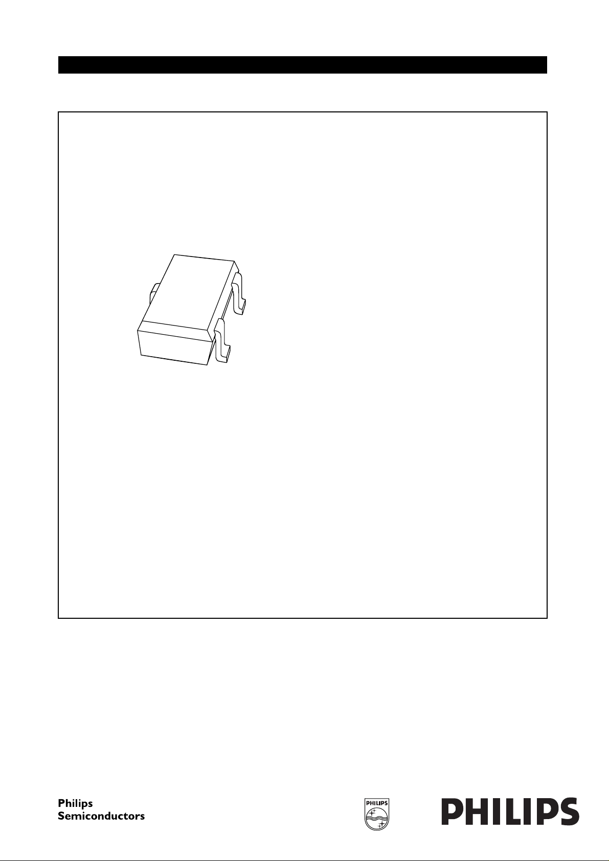
DESCRIPTION
Planar Schottky barrier diodes
encapsulated in an SC-70 very small
plastic SMD package. Single diodes
and double diodes with different
pinning are available.
MARKING
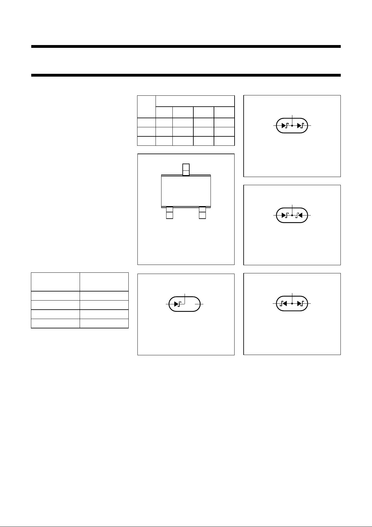
PINNING
1PS70SB..
PIN
40 44 45 46
1a
2 n.c. k
a1a1k
1
a
2
2
3k1k1,a2k1,k2a1,a
alfpage
Top view
3
1
2
MGD765
Fig.1 Simplified outline
(SC-70) and pin
configuration.
1
k
2
3
12
MLC358
2
Fig.3 1PS70SB44 diode
configuration (symbol).
3
12
MLC359
Fig.4 1PS70SB45 diode
configuration (symbol).
TYPE NUMBER
MARKING
CODE
1PS70SB40 6∗3
1PS70SB44 6∗4
1PS70SB45 6∗5
1PS70SB46 6∗6
Note
1. ∗ = -: Made in Hong Kong.
∗ = t: Made in Malaysia.
(1)
3
12
n.c.
MLC357
Fig.2 1PS70SB40 single
diode configuration
(symbol).
3
12
MLC360
Fig.5 1PS70SB46 diode
configuration (symbol).
1999 Apr 26 2
Philips Semiconductors Product specification
Schottky barrier (double) diodes 1PS70SB40 series
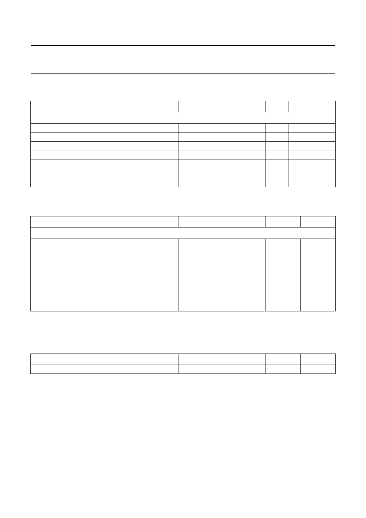
LIMITING VALUES
In accordance with the Absolute Maximum Rating System (IEC 134).
SYMBOL PARAMETER CONDITIONS MIN. MAX. UNIT
Per diode
V
R
I
F
I
FRM
I
FSM
T
stg
T
j
T
amb
ELECTRICAL CHARACTERISTICS
=25°C unless otherwise specified.
T
amb
continuous reverse voltage − 40 V
continuous forward current − 120 mA
repetitive peak forward current tp≤ 1s; δ≤0.5 − 120 mA
non-repetitive peak forward current tp<10ms − 200 mA
storage temperature −65 +150 °C
junction temperature − 150 °C
operating ambient temperature −65 +150 °C
SYMBOL PARAMETER CONDITIONS MAX. UNIT
Per diode
V
F
I
R
τ charge carrier life time I
C
d
continuous forward voltage see Fig.6
I
= 1 mA 380 mV
F
I
= 10 mA 500 mV
F
I
=40mA 1 V
F
continuous reverse current VR= 30 V; note 1; see Fig.7 1 µA
V
= 40 V; note 1; see Fig.7 10 µA
R
= 5 mA; Krakauer method 100 ps
F
diode capacitance VR= 0; f = 1 MHz; see Fig.9 5 pF
Note
1. Pulse test: t
= 300 µs; δ = 0.02.
p
THERMAL CHARACTERISTICS
SYMBOL PARAMETER CONDITIONS VALUE UNIT
R
th j-a
thermal resistance from junction to ambient note 1 625 K/W
Note
1. Refer to SC70 standard mounting conditions.
1999 Apr 26 3
 Loading...