Philips 19PFL3403-10 Schematic

Colour Television Chassis
TPS1.2E
LA
I_17620_000.eps
260308
Contents Page Contents Page
1. Technical Specifications, Connections, and Chassis
Overview 2
2. Safety Instructions, Warnings, and Notes 4
3. Directions for Use 5
4. Mechanical Instructions 6
5. Service Modes, Error Codes, and Fault Finding 11
6. Block Diagrams, Test Point Overview, and
Waveforms
Wiring Diagram19PFL3403 15
Block Diagram Scaler Board 19PFL3403 16
7. Circuit Diagrams and PWB Layouts Diagram PWB
19PFL3403 Power Board Adapter (PB01) 17 19
19PFL3403 Power Board Inverter (PB02) 18 19
Scaler Board: Video Input (SB01) 20 30-31
Scaler Board: SCART & YPbPr (SB02) 21 30-31
Scaler Board: VGA (SB03) 22 30-31
Scaler Board: HDMI Input (SB04) 23 30-31
Scaler Board: Panel I/F (SB05) 24 30-31
Scaler Board: MST9x980
Scaler Board: DDR & SDRAM (SB07) 26 30-31
Scaler Board: Audio Amplifier (SB08) 27 30-31
Scaler Board: Power (SB09) 28 30-31
Scaler Board: Sub MCU (SB10) 29 30-31
Keyboard & Control Panel (KB01) 32 33
IR & LED Panel (IB01) 34 35
8. Alignments 37
9. Circuit Descriptions, Abbreviation List, and IC Data
Sheets 39
Abbreviation List 40
IC Data Sheets 42
10. Spare Parts List 49
11. Revision List 56
(SB06) 25 30-31
©
Copyright 2008 Philips Consumer Electronics B.V. Eindhoven, The Netherlands.
All rights reserved. No part of this publication may be reproduced, stored in a
retrieval system or transmitted, in any form or by any means, electronic,
mechanical, photocopying, or otherwise without the prior permission of Philips.
Published by CS 0864 BG CD Consumer Care Printed in the Netherlands Subject to modification EN 3122 785 17600

EN 2 TPS1.2E LA1.
Technical Specifications, Connections, and Chassis Overview
1. Technical Specifications, Connections, and Chassis Overview
Index of this chapter:
1.1 Technical Specifications
1.2 Connection Overview
1.3 Chassis Overview
Notes:
• Figures can deviate due to the different set executions.
• Specifications are indicative (subject to change).
1.1 Technical Specifications
1.1.1 Vision
Display type : LCD
Screen Size : 19"
Display area (mm) : 408.2 (H) x 255.2 (V)
Number of Pixel : 1440 (H) x 900 (V)
Pitch (mm) : 0.2835x 0.2835
Colour pixel arrangement : RGB vertical stripe
Display operating mode : TN Mode, Normally
White
Colour depth : 16.7M colours (RGB
6-bits + HiFRC)
Brightness (cd/m^2) : 300 cd/m2 (typ)
Viewing angle : R/L 170, U/D 160 (typ)
Surface treatment : Hard coating (3H), AG
(Haze 25%)
Electrical interface : Dual Channel LVDS
Response time (ms, typ) : 5ms (typ)
Contrast ratio : Typical 1000:1
Backlight : 4 EEFL
Support Video Formats : 720 x 400@ 70Hz
: 640 x 480@ 60Hz
: 640 x 480@ 67Hz
: 800 x 600@ 60Hz
: 1024 x 768@ 60Hz
: 1280 x 960@ 60Hz
: 1440 x 900@ 60Hz
1.1.2 Sound
Sound systems : Virtual Surround
Maximum power (W) : 3Wx2
1.1.3 Miscellaneous
Power supply:
Power consumption : 47 W
AC line voltage range : 90~264 V
AC line frequency range : 50 - 60 Hz
Inrush current : < 40 A at 240 Vac
when cold start
Leakage current : < 0.5 mA at 240 Vac
Horizontal scan:
Horizontal : 30~81 kHz
Vertical : 56~76 Hz
1.2 Connection Overview
1.2.1 Rear Connections
VGA: Video RGB - In
1
5
10
6
15
11
E_06532_002.eps
050404
Figure 1-1 VGA Connector
1 - Video Red 0.7 V
2 - Video Green 0.7 V
3 - Video Blue 0.7 V
4-n.c.
5 - Ground Gnd H
6 - Ground Red Gnd H
7 - Ground Green Gnd H
8 - Ground Blue Gnd H
9-+5V
+5 V j
DC
10 - Ground Sync Gnd H
11 - n.c.
12 - DDC_SDA DDC data j
13 - H-sync 0 - 5 V j
14 - V-sync 0 - 5 V j
15 - DDC_SCL DDC clock j
HDMI: Digital Video, Digital Audio - In
19
18 2
Figure 1-2 HDMI (type A) connector
1 - D2+ Data channel j
2 - Shield Gnd H
3 - D2- Data channel j
4 - D1+ Data channel j
5 - Shield Gnd H
6 - D1- Data channel j
7 - D0+ Data channel j
8 - Shield Gnd H
9 - D0- Data channel j
10 - CLK+ Data channel j
11 - Shield Gnd H
12 - CLK- Data channel j
13 - CEC
14 - n.c.
15 - DDC_SCL DDC clock j
16 - DDC_SDA DDC data jk
17 - Ground Gnd H
18 - +5V j
19 - HPD Hot Plug Detect j
20 - Ground Gnd H
/ 75 ohm j
PP
/ 75 ohm j
PP
/ 75 ohm j
PP
1
E_06532_017.eps
250505
Box (WxDxH, mm) : 512 x 136 x 458
Product (with stand) (HxWxD, mm) : 392.3 x 467.3 x 69.3
Technical Specifications, Connections, and Chassis Overview
1.3 Chassis Overview
EN 3TPS1.2E LA 1.
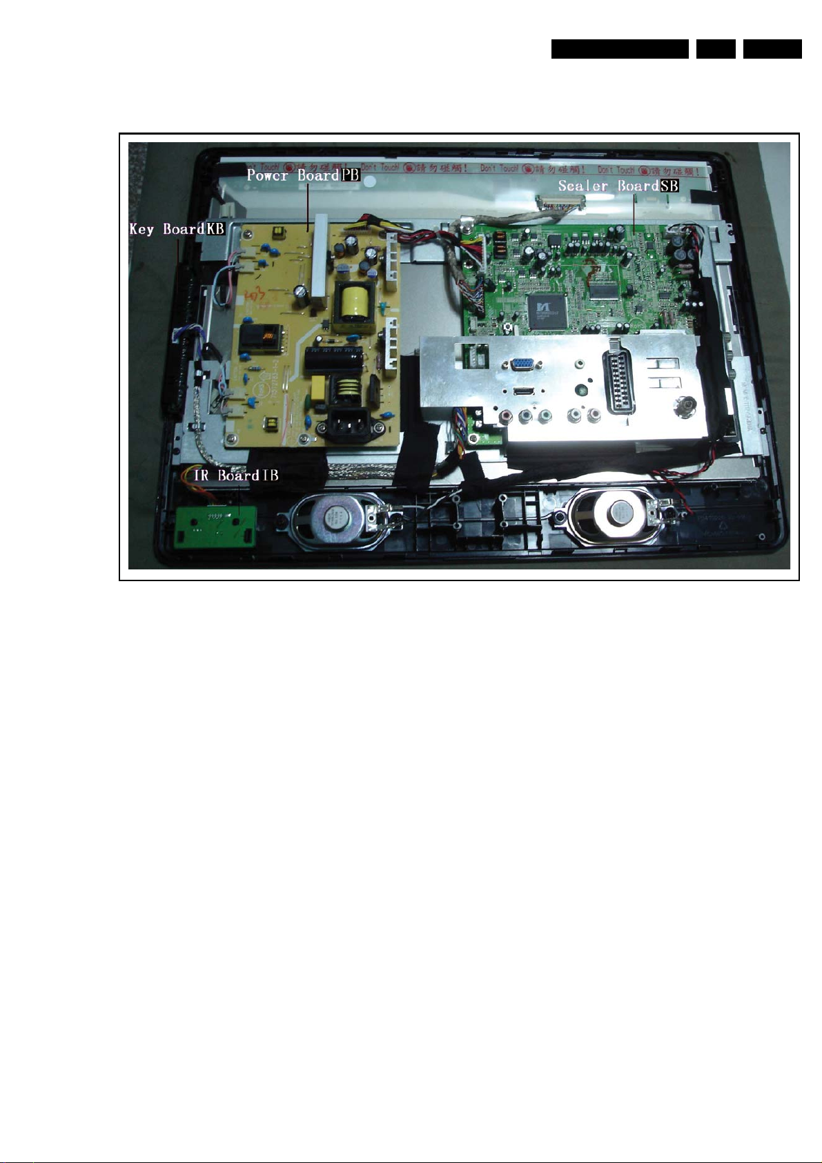
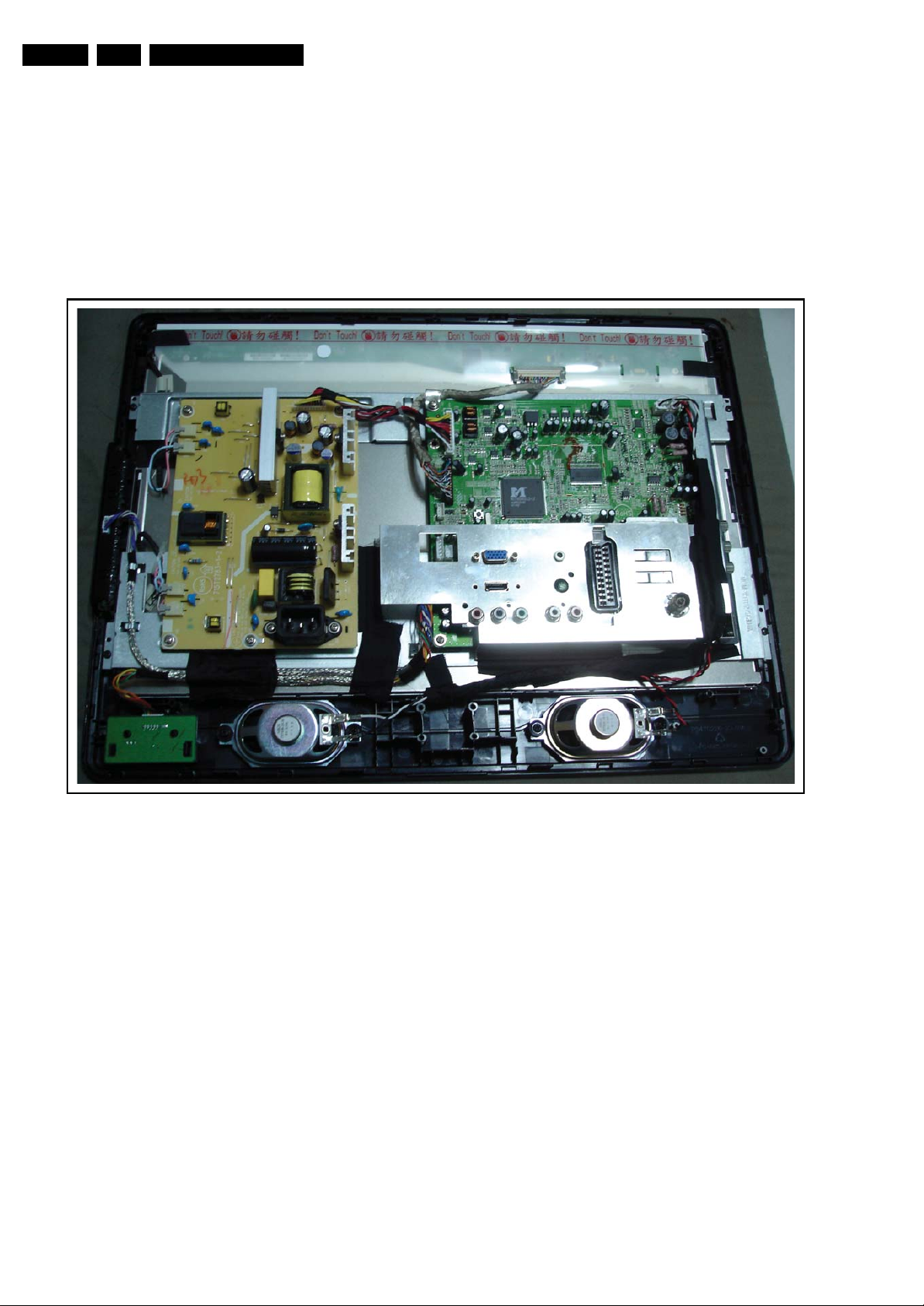
Figure 1-3 Chassis Overview (19PFL3403)
I_17600_021.eps
010408

EN 4 TPS1.2E LA2.
Safety Instructions, Warnings, and Notes
2. Safety Instructions, Warnings, and Notes
Index of this chapter:
2.1 Safety Instructions
2.2 Warnings
2.3 Notes
2.1 Safety Instructions
Safety regulations require the following during a repair:
• Connect the set to the Mains/AC Power via an isolation
transformer (> 800 VA).
• Replace safety components, indicated by the symbol h,
only by components identical to the original ones. Any
other component substitution (other than original type) may
increase risk of fire or electrical shock hazard.
Safety regulations require that after a repair, the set must be
returned in its original condition. Pay in particular attention to
the following points:
• Route the wire trees correctly and fix them with the
mounted cable clamps.
• Check the insulation of the Mains/AC Power lead for
external damage.
• Check the strain relief of the Mains/AC Power cord for
proper function.
• Check the electrical DC resistance between the Mains/AC
Power plug and the secondary side (only for sets that have
a Mains/AC Power isolated power supply):
1. Unplug the Mains/AC Power cord and connect a wire
between the two pins of the Mains/AC Power plug.
2. Set the Mains/AC Power switch to the "on" position
(keep the Mains/AC Power cord unplugged!).
3. Measure the resistance value between the pins of the
Mains/AC Power plug and the metal shielding of the
tuner or the aerial connection on the set. The reading
should be between 4.5 Mohm and 12 Mohm.
4. Switch "off" the set, and remove the wire between the
two pins of the Mains/AC Power plug.
• Check the cabinet for defects, to prevent touching of any
inner parts by the customer.
2.2 Warnings
• All ICs and many other semiconductors are susceptible to
electrostatic discharges (ESD w). Careless handling
during repair can reduce life drastically. Make sure that,
during repair, you are connected with the same potential as
the mass of the set by a wristband with resistance. Keep
components and tools also at this same potential. Available
ESD protection equipment:
– Complete kit ESD3 (small tablemat, wristband,
connection box, extension cable and earth cable) 4822
310 10671.
– Wristband tester 4822 344 13999.
• Be careful during measurements in the high voltage
section.
• Never replace modules or other components while the unit
is switched "on".
• When you align the set, use plastic rather than metal tools.
This will prevent any short circuits and the danger of a
circuit becoming unstable.
2.3 Notes
2.3.1 General
• Measure the voltages and waveforms with regard to the
chassis (= tuner) ground (H), or hot ground (I), depending
on the tested area of circuitry. The voltages and waveforms
shown in the diagrams are indicative. Measure them in the
Service Default Mode (see chapter 5) with a colour bar
signal and stereo sound (L: 3 kHz, R: 1 kHz unless stated
otherwise) and picture carrier at 475.25 MHz for PAL, or
61.25 MHz for NTSC (channel 3).
• Where necessary, measure the waveforms and voltages
with (D) and without (E) aerial signal. Measure the
voltages in the power supply section both in normal
operation (G) and in stand-by (F). These values are
indicated by means of the appropriate symbols.
2.3.2 Schematic Notes
• All resistor values are in ohms, and the value multiplier is
often used to indicate the decimal point location (e.g. 2K2
indicates 2.2 kohm).
• Resistor values with no multiplier may be indicated with
either an "E" or an "R" (e.g. 220E or 220R indicates 220
ohm).
• All capacitor values are given in micro-farads (μ= x10
nano-farads (n= x10
• Capacitor values may also use the value multiplier as the
decimal point indication (e.g. 2p2 indicates 2.2 pF).
• An "asterisk" (*) indicates component usage varies. Refer
to the diversity tables for the correct values.
• The correct component values are listed in the Spare Parts
List. Therefore, always check this list when there is any
doubt.
2.3.3 BGA (Ball Grid Array) ICs
Introduction
For more information on how to handle BGA devices, visit this
URL: www.atyourservice.ce.philips.com (needs subscription,
not available for all regions). After login, select “Magazine”,
then go to “Repair downloads”. Here you will find Information
on how to deal with BGA-ICs.
BGA Temperature Profiles
For BGA-ICs, you must use the correct temperature-profile,
which is coupled to the 12NC. For an overview of these profiles,
visit the website www.atyourservice.ce.philips.com (needs
subscription, but is not available for all regions)
You will find this and more technical information within the
"Magazine", chapter "Repair downloads".
For additional questions please contact your local repair help
desk.
2.3.4 Lead-free Soldering
Due to lead-free technology some rules have to be respected
by the workshop during a repair:
• Use only lead-free soldering tin Philips SAC305 with order
code 0622 149 00106. If lead-free solder paste is required,
please contact the manufacturer of your soldering
equipment. In general, use of solder paste within
workshops should be avoided because paste is not easy to
store and to handle.
• Use only adequate solder tools applicable for lead-free
soldering tin. The solder tool must be able:
– To reach a solder-tip temperature of at least 400°C.
– To stabilize the adjusted temperature at the solder-tip.
– To exchange solder-tips for different applications.
• Adjust your solder tool so that a temperature of around
360°C - 380°C is reached and stabilized at the solder joint.
Heating time of the solder-joint should not exceed ~ 4 sec.
Avoid temperatures above 400°C, otherwise wear-out of
tips will increase drastically and flux-fluid will be destroyed.
To avoid wear-out of tips, switch “off” unused equipment or
reduce heat.
-9
), or pico-farads (p= x10
-12
-6
),
).

Directions for Use
EN 5TPS1.2E LA 3.
• Mix of lead-free soldering tin/parts with leaded soldering
tin/parts is possible but PHILIPS recommends strongly to
avoid mixed regimes. If this cannot be avoided, carefully
clear the solder-joint from old tin and re-solder with new tin.
2.3.5 Alternative BOM identification
The third digit in the serial number (example:
AG2B0335000001) indicates the number of the alternative
B.O.M. (Bill Of Materials) that has been used for producing the
specific TV set. In general, it is possible that the same TV
model on the market is produced with e.g. two different types
of displays, coming from two different suppliers. This will then
result in sets which have the same CTN (Commercial Type
Number; e.g. 28PW9515/12) but which have a different B.O.M.
number.
By looking at the third digit of the serial number, one can
identify which B.O.M. is used for the TV set he is working with.
If the third digit of the serial number contains the number “1”
(example: AG1B033500001), then the TV set has been
manufactured according to B.O.M. number 1. If the third digit is
a “2” (example: AG2B0335000001), then the set has been
produced according to B.O.M. no. 2. This is important for
ordering the correct spare parts!
For the third digit, the numbers 1...9 and the characters A...Z
can be used, so in total: 9 plus 26= 35 different B.O.M.s can be
indicated by the third digit of the serial number.
Identification: The bottom line of a type plate gives a 14-digit
serial number. Digits 1 and 2 refer to the production centre (e.g.
AG is Bruges), digit 3 refers to the B.O.M. code, digit 4 refers
to the Service version change code, digits 5 and 6 refer to the
production year, and digits 7 and 8 refer to production week (in
example below it is 2006 week 17). The 6 last digits contain the
serial number.
MODEL :
PROD.NO:
32PF9968/10
AG 1A0617 000001
MADE IN BELGIUM
220-240V 50/60Hz
~
VHF+S+H+UHF
S
128W
BJ3.0E LA
E_06532_024.eps
260308
Figure 2-1 Serial number (example)
2.3.6 Board Level Repair (BLR) or Component Level Repair (CLR)
If a board is defective, consult your repair procedure to decide
if the board has to be exchanged or if it should be repaired on
component level.
If your repair procedure says the board should be exchanged
completely, do not solder on the defective board. Otherwise, it
cannot be returned to the O.E.M. supplier for back charging!
2.3.7 Practical Service Precautions
• It makes sense to avoid exposure to electrical shock.
While some sources are expected to have a possible
dangerous impact, others of quite high potential are of
limited current and are sometimes held in less regard.
• Always respect voltages. While some may not be
dangerous in themselves, they can cause unexpected
reactions that are best avoided. Before reaching into a
powered TV set, it is best to test the high voltage insulation.
It is easy to do, and is a good service precaution.
3. Directions for Use
You can download this information from the following websites:
http://www.philips.com/support
http://www.p4c.philips.com
EN 6 TPS1.2E LA4.
Mechanical Instructions
4. Mechanical Instructions
Index of this chapter:
4.1 Cable Dressing
4.2 Service Positions
4.3 Assy/Panel Removal
4.4 Set Re-assembly
4.1 Cable Dressing
Notes:
• Figures below can deviate slightly from the actual situation,
due to the different set executions.
• Follow the disassembly instructions in the described order.
Figure 4-1 Cable dressing (19PFL3403)
I_17600_003.eps
010408
Mechanical Instructions
EN 7TPS1.2E LA 4.
4.2 Service Positions
For easy servicing of this set, there are a few possibilities
created:
• The buffers from the packaging (see figure "Rear cover").
• Foam bars (created for Service).
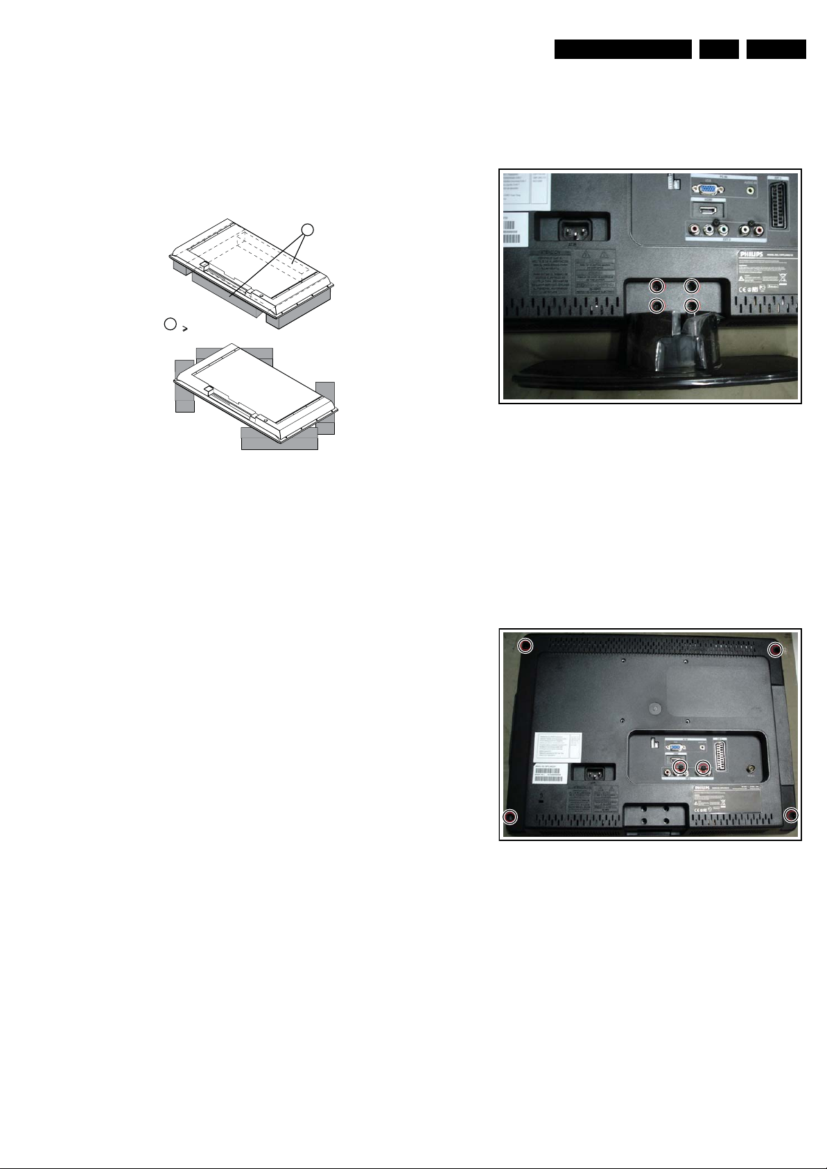
4.2.1 Foam Bars
1
Required for sets
1
42"
E_06532_018.eps
171106
Figure 4-2 Foam bars
4.3 Assy/Panel Removal
4.3.1 Stand Assy
Unscrew the marked screws to remove the stand assy.
Figure 4-3 Remove Stand ASSY
4.3.2 Rear Cover
I_17600_004.eps
010408
The foam bars (order code 3122 785 90580 for two pieces) can
be used for all types and sizes of Flat TVs. See figure “Foam
bars” for details. Sets with a display of 42” and larger, require
four foam bars [1]. Ensure that the foam bars are always
supporting the cabinet and never only the display. Caution:
Failure to follow these guidelines can seriously damage the
display!
By laying the TV face down on the (ESD protective) foam bars,
a stable situation is created to perform measurements and
alignments. By placing a mirror under the TV, you can monitor
the screen.
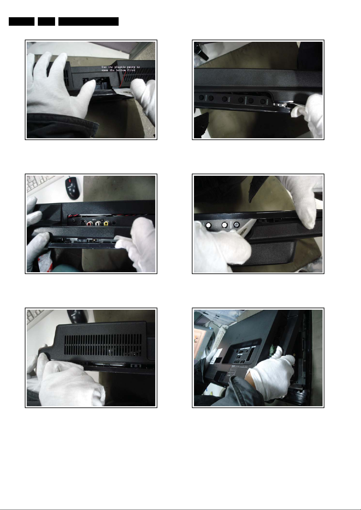
1. Remove the six marked screws that secure the rear cover.
2. Pay attention to the internal hooks while removing the rear
cover. Use e.g. a plastic putty knife to release the hooks on
the bottom, the top, the left and the right side, then you can
easily remove the rear cover from the bezel.
Please refer to the photos attached below and next page.
This a good method to open the rear cover and avoid
causing scratches.
I_17600_014.eps
010408
Figure 4-4 Remove Rear Cover (1)
EN 8 TPS1.2E LA4.
Mechanical Instructions
Figure 4-5 Remove Rear Cover (2)
Figure 4-6 Remove Rear Cover (3)
I_17600_015.eps
010408
I_17600_016.eps
010408
Figure 4-8 Remove Rear Cover (5)
Figure 4-9 Remove Rear Cover (6)
I_17600_018.eps
010408
I_17600_019.eps
010408
Figure 4-7 Remove Rear Cover (4)
I_17600_017.eps
010408
Figure 4-10 Remove Rear Cover (7)
I_17600_020.eps
010408
Mechanical Instructions
EN 9TPS1.2E LA 4.
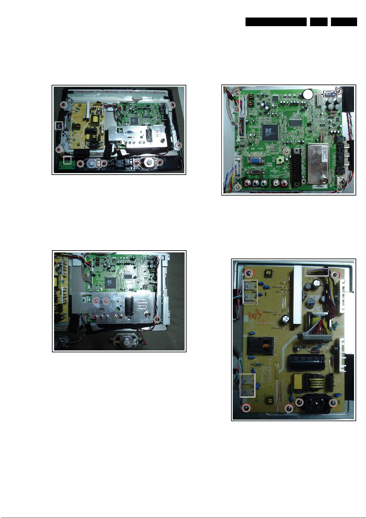
4.3.3 Bezel
1. Refer to the next figure.
2. Unplug marked connectors.
3. Release the marked screws and remove the bezel.
When defective, replace the whole unit.
Figure 4-11 Bezel
4.3.4 Shielding-EMI
1. Refer to next figure.
2. Release the marked screws and remove the shielding.
When defective, replace the whole unit.
I_17600_005.eps
010408
4.3.5 Main Board
1. Refer to next figure.
2. Unplug all connectors.
3. Remove the marked screws and then remove the main
board.
When defective, replace the whole unit.
(2x)
Figure 4-13 Main Board
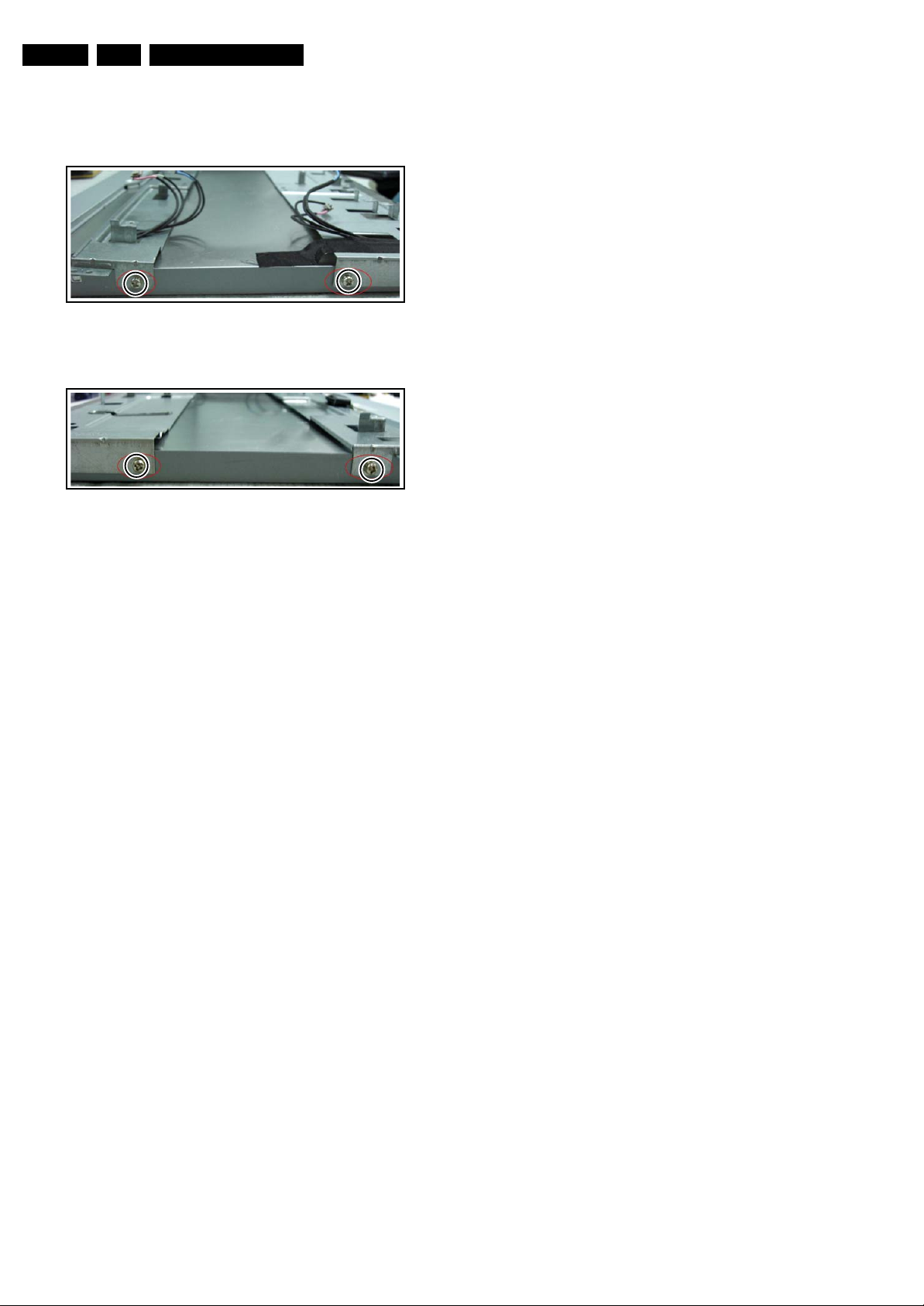
4.3.6 Power Board
1. Refer to next figure. Unplug the connectors.
2. Unscrew the marked screws to remove the power board.
I_17620_007.eps
250308
Figure 4-12 EMI Shielding
I_17600_006.eps
010408
Figure 4-14 Power Board
I_17600_022.eps
010408
EN 10 TPS1.2E LA4.
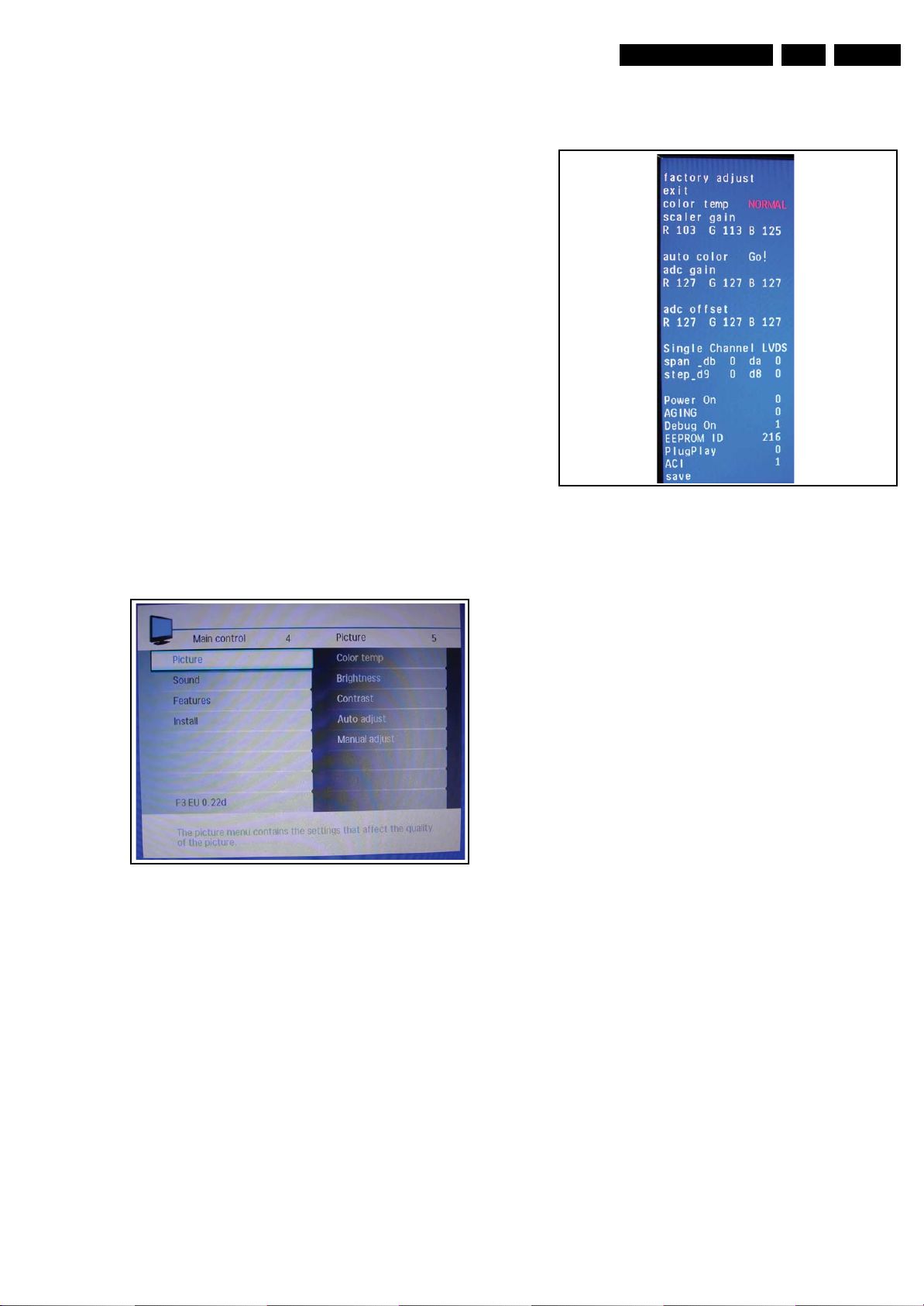
4.3.7 Bracket
1. Refer to next two figures.
2. Remove the screws remarked in red.
Figure 4-15 Bracket1
Mechanical Instructions
I_17600_007.eps
010408
I_17600_008.eps
010408
Figure 4-16 Bracket2
4.4 Set Re-assembly
To re-assemble the whole set, execute all processes in reverse
order.
Notes:
• While re-assembling, make sure that all cables are placed
and connected in their original position. See figure "Cable
dressing".
Service Modes, Error Codes, and Fault Finding
5. Service Modes, Error Codes, and Fault Finding
Index of this chapter:
5.1 Test Points
5.2 Service Mode
5.3 Service Tools
5.4 Tips and Tricks
5.1 Test Points
This chassis is NOT equipped with test points in the service
printing.
5.2 Service Mode
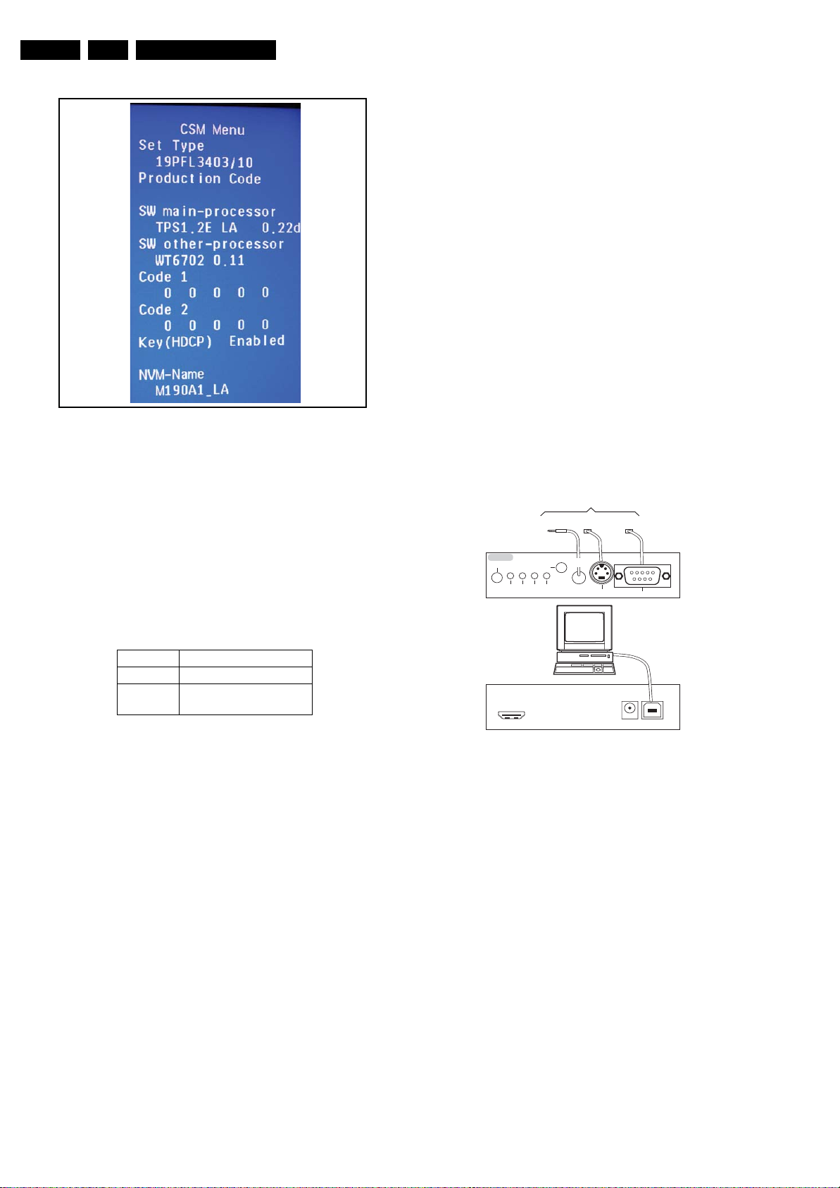
5.2.1 Factory Mode
How to Enter
To enter the Factory mode, use one of the following methods:
• Turn on the monitor, press the “menu” key.
• Press remote control code ”062596”, then press “Info [i+]”
key. When you press the “menu” key again, the OSD
will show as below, then you can just select “F3 EU
0.22d” to carry out the factory OSD.
Caution: This function is available for development and
service personnel only, not for end customers.
After entering factory mode, the following screen is visible, the
values can be adjusted according to the requested.
How to EXIT
Choose ‘EXIT”, then press “OK” button on remote control.
Figure 5-2 Factory mode menu 2
EN 11TPS1.2E LA 5.
I_17600_010.eps
010408
Figure 5-1 Factory mode menu 1
I_17600_009.eps
010408
5.2.2 Customer Service Mode (CSM)
Purpose
When a customer is having problems with his TV-set, he can
call his dealer or the Customer Helpdesk. The service
technician can then ask the customer to activate the CSM, in
order to identify the status of the set. Now, the service
technician can judge the severity of the complaint. In many
cases, he can advise the customer how to solve the problem,
or he can decide if it is necessary to visit the customer. The
CSM is a read only mode; therefore, modifications in this mode
are not possible.
How to Activate CSM
Press the “menu” key and key in the code”123654” via the
standard RC transmitter.
How to Navigate
By means of the “CURSOR-DOWN/UP” knob on the RCtransmitter on the screen.
EN 12 TPS1.2E LA5.
Service Modes, Error Codes, and Fault Finding
Contents of CSM
I_17600_011.eps
010408
Figure 5-3 CSM Menu (19PFL3403)
Menu Explanation
1. Set Type: Type number and region.
2. Production code: Product serial no.
3. SW main-processor: SW-naming of Mstar/Trident, see
format in generic service document.
4. SW other-processor: if valid.
5. Code 1: Logging I2C error codes in NVM/EEPROM (5 last
logged errors).
6. Code 2: Logging I2C error codes in NVM/EEPROM (5 first
logged errors).
For the data of the Code 1/2, please refer to the table as
below.
Error Code Error Code Type
00 OK
04 The checksum for
EEPROM failed
7. Key (HDCP): Indicates if the HDCP-key are valid.
8. NVM-Name: Indicates the used LCD panel type and region
(NVM content and main SW depend on the used LCD
panel).
How to exit
Press ”MENU” on the RC-transmitter.
5.3 Service Tools
5.3.1 ComPair
Introduction
ComPair (Computer Aided Repair) is a Service tool for Philips
Consumer Electronics products. and offers the following:
1. ComPair helps you to quickly get an understanding on how
to repair the chassis in a short and effective way.
2. ComPair allows very detailed diagnostics and is therefore
capable of accurately indicating problem areas. You do not
have to know anything about I
yourself, because ComPair takes care of this.
3. ComPair speeds up the repair time since it can
automatically communicate with the chassis (when the uP
is working) and all repair information is directly available.
4. ComPair features TV software upgrade possibilities.
Specifications
ComPair consists of a Windows based fault finding program
and an interface box between PC and the (defective) product.
The (new) ComPair II interface box is connected to the PC via
an USB cable. For the TV chassis, the ComPair interface box
and the TV communicate via a bi-directional cable via the
service connector(s).
How to Connect
This is described in the ComPair chassis fault finding database.
TO
UART SERVICE
CONNECTOR
CONNECTOR
ComPair II
RC in
Optional
Switch
Power ModeLink/
Activity
HDMI
I
2
C only
RC out
Multi
function
Figure 5-4 ComPair II interface connection
Caution: It is compulsory to connect the TV to the PC as
shown in the picture above (with the ComPair interface in
between), as the ComPair interface acts as a level shifter. If
one connects the TV directly to the PC (via UART), ICs will be
blown!
TO TV
TO
UART SERVICE
I2C SERVICE
CONNECTOR
2
C
I
PC
ComPair II Developed by Philips Brugge
Optional power
5V DC
2
C or UART commands
TO
RS232 /UART
E_06532_036.eps
150208
How to Order
ComPair II order codes:
• ComPair II interface: 3122 785 91020.
• For SW see Philips service website.
•ComPair I
2
C interface cable: 9965 100 09269.
Note: If you encounter any problems, contact your local
support desk.
Service Modes, Error Codes, and Fault Finding
5.4 Tips and Tricks
Below find some repair tips and tricks.
5.4.1 Soft Reset
When a consumer has forgotten his lock code, you can set the
TV back in Virgin mode by keying in the code”978450” via the
standard RC transmitter. The NVM is not erased.
The standard unlock code will then be “0711”.
5.4.2 Hard Reset (erase NVRAM)
A hard reset is executed by together pressing the “P+” and “V+”
buttons on the TV, while unplugging and replugging the mains
cord.
Note: By using this hard reset mode, the TV will be brought
back in Virgin mode, but also all TV settings will be erased!
TV must completely be re-aligned via the “Factory” mode.
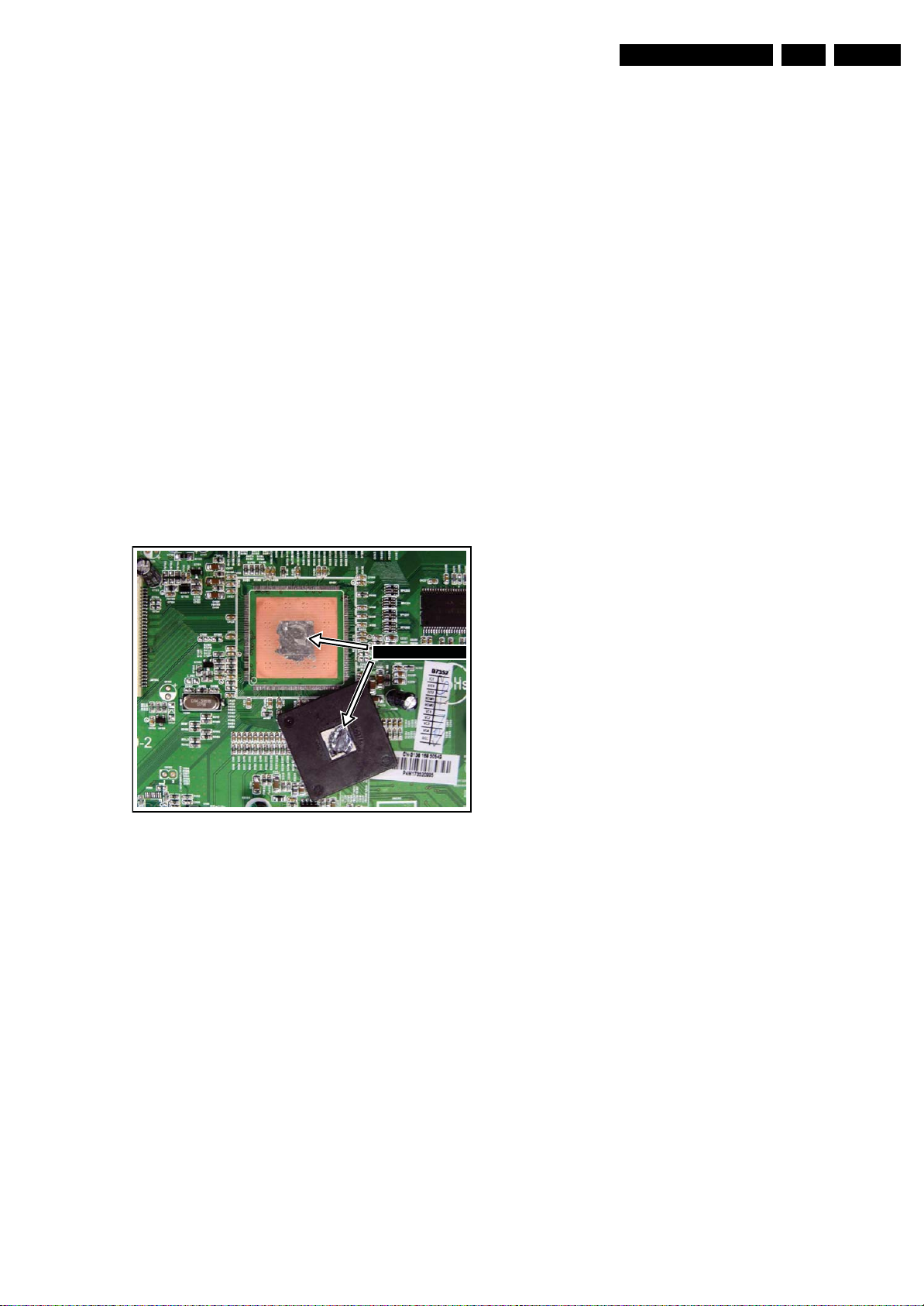
5.4.3 Removal of Morning Star Microprocessor
The Morning Star uP is fitted with a so-called E-pad (see photo
below). This is an extra surface for cooling and grounding. This
E-pad is soldered to the PWB.
To remove/place this IC on the PWB, use dedicated
equipment.
EN 13TPS1.2E LA 5.
Soldered E-Pad
I_17620_046.eps
Figure 5-5 E-pad (photo from TPS1.0 chassis)
280308

EN 14 TPS1.2E LA5.
Personal Notes:
Service Modes, Error Codes, and Fault Finding
E_06532_012.eps
131004
Block Diagrams, Test Point Overview, and Waveforms
6. Block Diagrams, Test Point Overview, and Waveforms
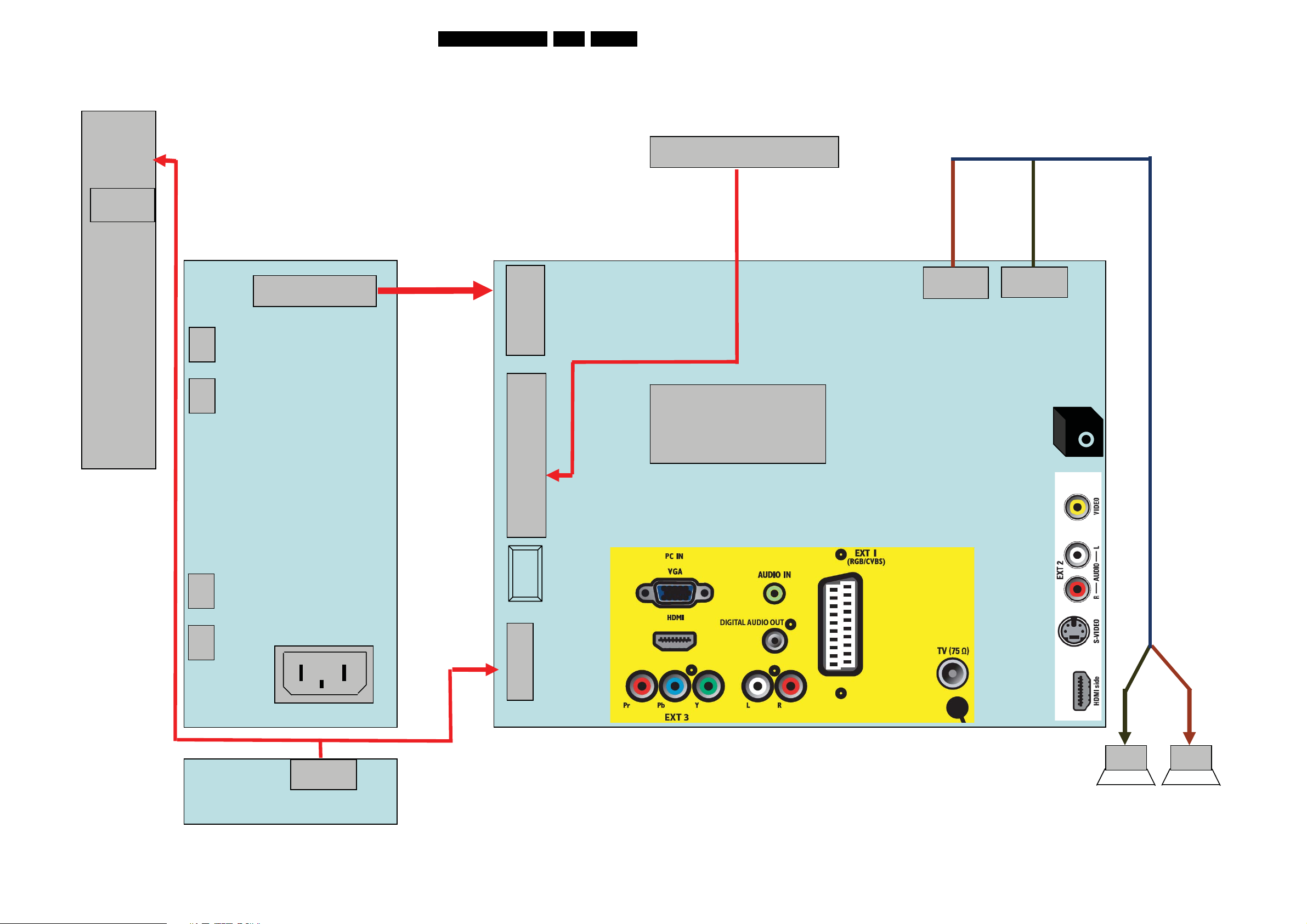
Wiring Diagram19PFL3403
15TPS1.2E LA 6.
Key
Board
5 Pin
CN101
Panel
095T8013 3D 72
095T8013 2D 73
5
LVDS Cable
1
11
11 Pin
CN902
CN802
1
12
CN702
12 Pin
3 Pin 2Pin
2131
1
095T801830D168
CN602
CN601
30
CN801
CN108
30 Pin
MST98980CLD-LF
U401
Head Phone
Power Board
CN804
CN803
IR Board
AC IN
CN901
1
6 Pin
CN1
Main Board
VIDEO
1
AUDIO R/L
11
095T801411D 5
11Pin
S-VIDEO
CN401
HDMI
1
6
Speaker R/L
I_17600_001.eps
010408
Block Diagrams, Test Point Overview, and Waveforms
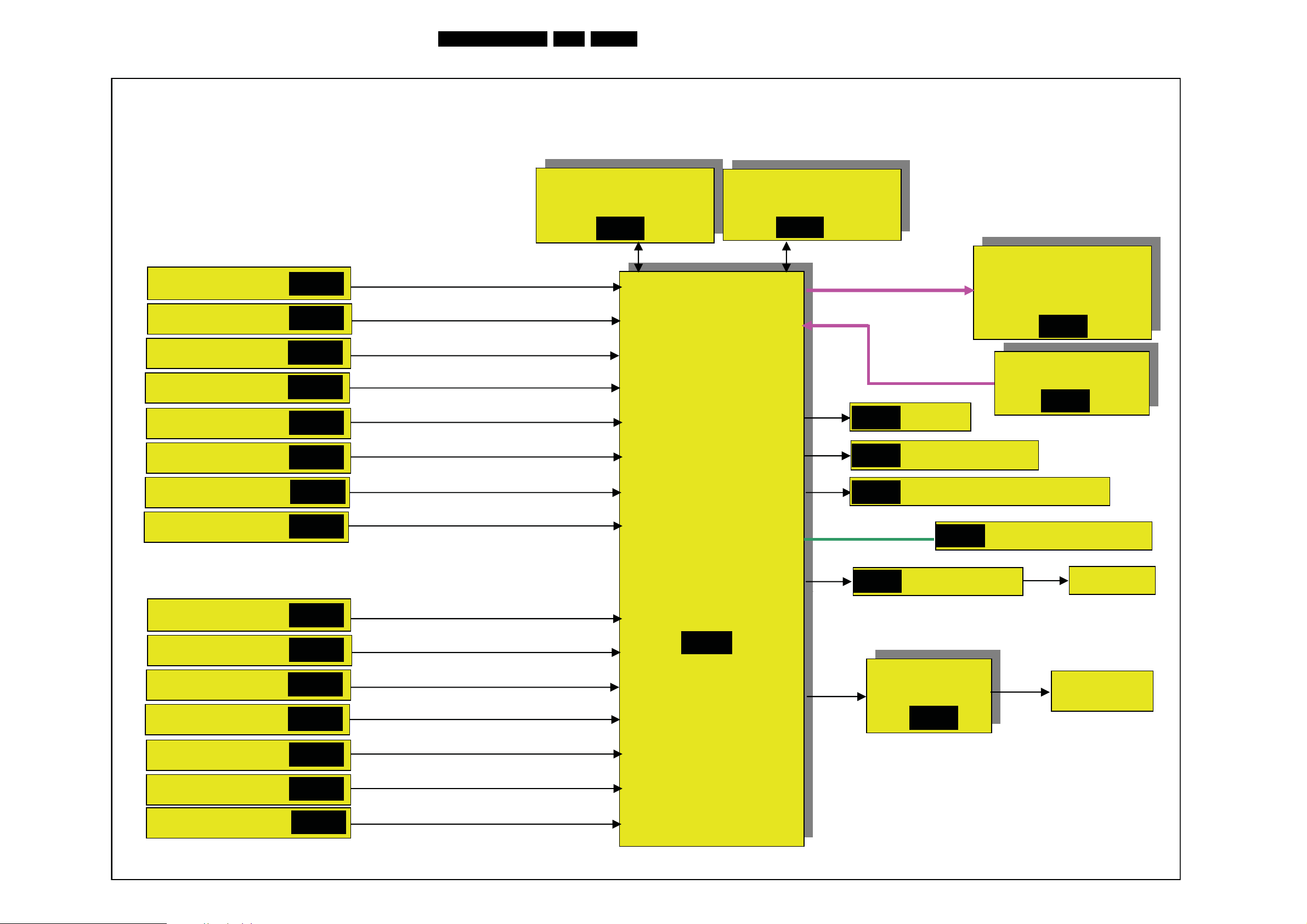
Block Diagram Scaler Board 19PFL3403
PHILIPS 19W ATV Block Diagram
16TPS1.2E LA 6.
Video Block
Tuner PACK
CVI
S_VIDEO
VGA
HDMI 1
HDMI 2
AV
SB-01
SB-02
SB-01
SB-03
SB-04
SB-04
SB-01
Tuner_CVBS
YPbPr
Y/C
PC(R,G,B&H,V)
CVBS
WT6702F_OG200WT
(Sub MCU)
SB-10
EM638165TS-6G
SB-07
SB-06
SB-06
SB-06
LVDS to panel
M190A1-L0A CMO
SB-05
INVERTER POWER
SB-09
KEY/IR
IR Receiver LED
Flash MX25L8005M2I-15G
SCART
HDMI-1
Audio Block
Tuner_SIF
CVI L/R
AVS_VIDEO L/R
PC AUDIO
HDMI 1
HDMI 2
SCART L/R
SB-02
SB-01
SB-01
SB-01
SB-08
SB-04
SB-04
SB-02
MST98980CLD
MST98980CLD
TV
TV
CONTROLLER
CONTROLLER
SB-06
2
I
C BUS
SB-08
SB-06
EARPHONE AMP
YDA148
SB-08
EEPROM AF24BC32
Headphone
speakers
I_17600_002.eps
010408
Circuit Diagrams and PWB Layouts
7. Circuit Diagrams and PWB Layouts
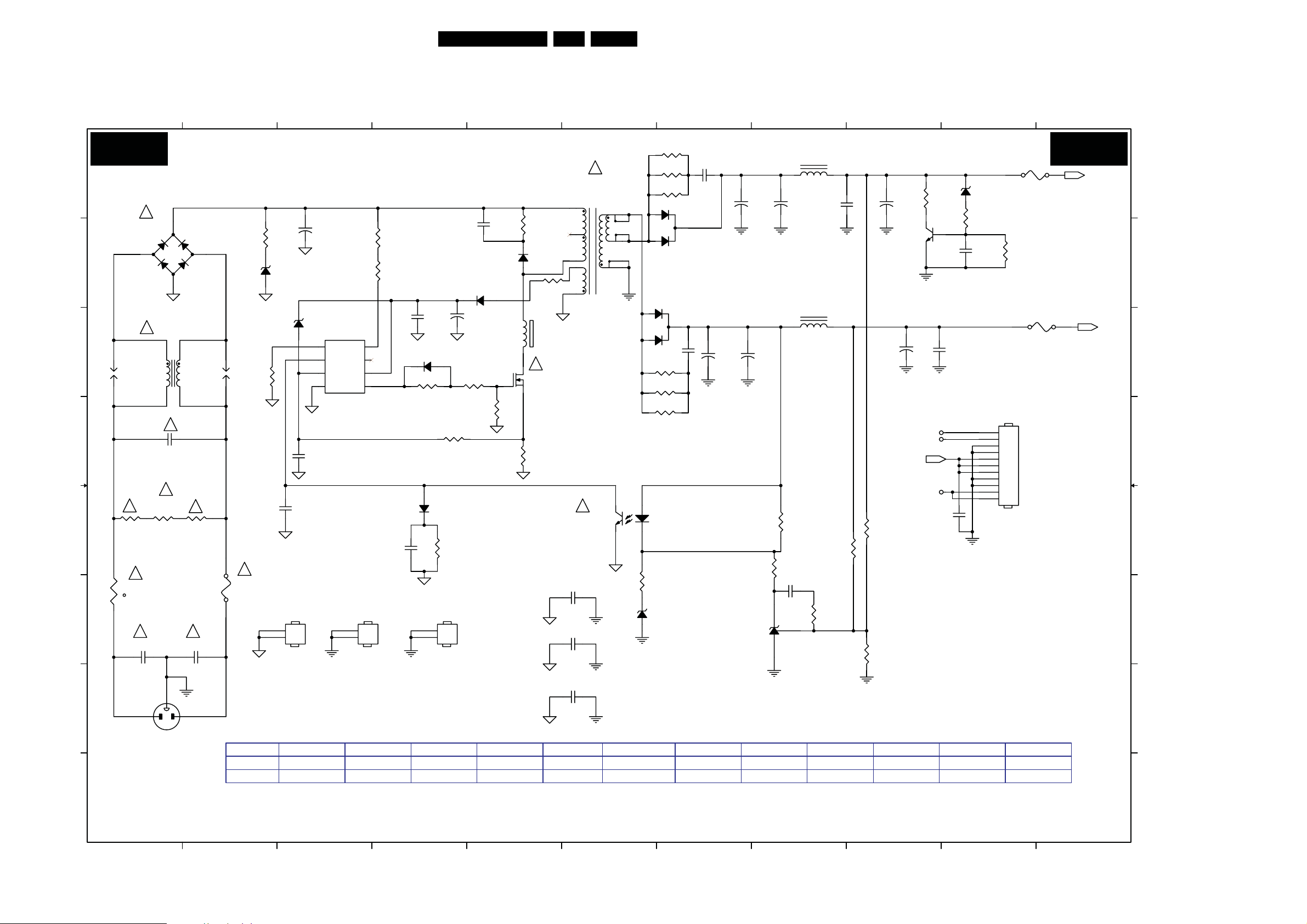
19PFL3403 Power Board Adapter
17TPS1.2E LA 7.
1
2
3
POWER BOARD: ADAPTER
PB01 PB01
A A
!
L902
!
L
73L 174 40LSG
C903
0.47UF
!
R902
620K 1/4W
1
+
-
4
1
4
SPARK GAP
2
3
!
!
R901
620K 1/4W
!
C902
0.001uF/250VAC
FG
3
12
2
SG902
R906
10R 1/4W
ZD903
P6KE440A
R941
100K 1/8W 1%
C923
470pF/25V
!
F901
FUSE
84G 56 4 B
ZD901
NC
HS1
HEAT SINK(Q901)
1
2
+
C905
120uF450VAC
67G315Z12115K
IC901
1
RT
2
COMP
3
CS
4
GND OUT
LD7575APS
56T 379107
C924
220pF
R904
8K2 1/4W
R905
8K2 1/4W
8
HV
7
NC
6
VCC
5
NC
HS2
HEAT SINK (D904)
1
2
BD901
GBU408
93G 50460900
3
B B
C C
SG901
SPARK GAP
D D
!
E E
F F
G G
R900
620K 1/4W
12
!
NR901
NTCR
61G 58 9T
t
!
C901
0.001uF/250VAC
C925
4
C919
0.1uF
D909
LL4148
R907
10R 1/8W
1
2
D910
NC
C906
2200pF 2KV
D902
FR103
93G 6038T52T
+
C908
22uF/50V
R912
10R 1/8W
R938
10K 1/8W
R922
200 1/8W
R931
NC
HS3
HEAT SINK(D906)
5
R908
100K 2W
D901
FR107
R909
3.3R 1/4W
12
FB901
Jumper
!
Q901
STP10NK70ZFP
57G 667 21
R914
0.39R 2W (19”)
0.36R 2W (22”)
T901
POWER X'FMR
80TL19T 33 N
4
5
6
3
2
!
IC903
PC123X2YFZOF
56G 139 3A
C931
0.001uF/250V
C907
NC
FG
C900
NC
FG
NC
8
L904
3.5uH
+
C918
L903
3.5uH
C920
0.1uF
9
+
C922
470uF/25V
PMBS3904
57G 417 4
C915
470uF/16V
Q903
+
R940
150R 2W
C916
0.1uF
6
R918
100R 1/4W
!
R919
7
C921
0.001uF
100R 1/4W
C914
+
C917
330uF/16V
+
C930
1000uF/16V
8
7
12
11
10
9
1
3
1
3
C929
0.001uF
R935
100R 1/4W
R903
R920
100R 1/4W
2
D906
YG865C15
93G 60268
D904
SP10100
93G 60267
2
+
1000uF/16V
10
ZD920
RLZ13B
R943
470R 1/8W
C932
0.001uF
F902
Jumper
R936
1K 1/4W
11
+12V
F903
+5V
Jumper
100R 1/4W
10
11
1
2
3
4
5
6
7
8
9
CN902
CONN
R934
100R 1/4W
12
43
R924
NC
R929
33K 1/8W 1%
DIM
ON/OFF
+5V
+12V
C927
0.1uF
R927
R937
NC
ZD902
NC
R925
150R 1/8W
IC902
KIA431VLA
56G 158 12
0.022uF/25V
C912
3K6 1/8W 1%
R928
0 1/8W
R930
2.43K 1/8W 1%
BD901 B1 CN901 G1
CN902 D10 C900 G6
C901 F1 C902 F2
C903 D1 C905 B3
C906 B5 C907 F6
C908 B4 C912 F8
C914 C7 C915 C9
C916 C9 C917 A7
C918 A8 C919 C4
C920 A8 C921 A7
C922 A9 C923 E2
C924 D3 C925 E4
C927 E10 C929 C7
C930 C7 C931 F6
C932 B10 D901 B5
D902 B4 D904 B6
D906 A6 D909 C4
D910 E4 FB901 C5
F901 E2 F902 A10
F903 C10 HS1 F3
HS2 F3 HS3 F4
IC901 C3 IC902 F8
IC903 E6 L902 C1
L903 C8 L904 A8
NR901 E1 Q901 C5
Q903 B9 R900 E1
R901 E2 R902 E1
R903 C6 R904 B3
R905 B3 R906 B2
R907 C4 R908 A5
R909 B5 R912 C4
R914 D5 R918 A6
R919 A6 R920 A6
R922 D4 R924 E8
R925 E8 R927 E8
R928 F8 R929 E9
R930 F9 R931 E4
R934 D6 R93
R936 B10 R937 E6
R938 C5 R940 A9
R941 C2 R943 A10
SG901 C1 SG902 C2
S4 F1 S5 F2
S6 E1 S7 E1
S8 D1 S9 E2
S10 E2 S11 D1
S12 C1 S14 A1
S15 C5 S16 E6
S17 A6 T901 A6
ZD901 C3 ZD902 F6
ZD903 B2 ZD920 A10
5 C6
CN901
SOCKET
H
1
MODE
22W ATV(12V)
22W DTV(16V)
2
ZD920
93G 39S 40 T
RLZ13B ROHM
93G 39S 44 T
RLZ18B
3
R929
61G0805330 2F
33K 1/8W 1%
61G0805430 2F
43K 1/8W 1%
T901
80TL19T 33 N
80TL22T 5 L
4
C917
67T 2043313KT
67G215S1024KV
5
C918
67G215S1024KV
C914 C930
NC 67T 2046
6
67G215S1023KV
812KT
7
D906
YG865C15RSC
93G 64 53 F
YG906C2RSC
86206 G39VK3201S512G76CN
H
I_17620_016.eps
8
9
10
010408
11
 Loading...