

Page 1
2N7002KDW
60V N-Channel Enhancement Mode MOSFET - ESD Protected
FEATURES
• R
, VGS@10V,IDS@500mA=3Ω
DS(ON)
• R
, VGS@4.5V,IDS@200mA=4Ω
DS(ON)
• Advanced Trench Process Technology
• High Density Cell Design For Ultra Low On-Resistance
• Very Low Leakage Current In Off Condition
• Specially Designed for Battery Operated Systems, Solid-State Relays
Drivers : Relays, Displays, Lamps, Solenoids, Memories, etc.
• ESD Protected 2KV HBM
• Lead free in comply with EU RoHS 2002/95/EC directives.
• Green molding compound as per IEC61249 Std. . (Halogen Free)
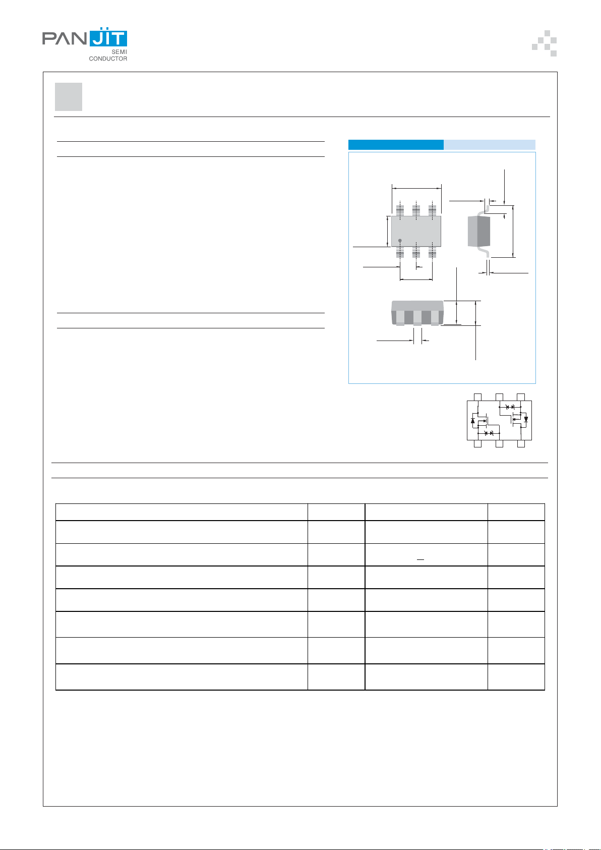
MECHANICAL DATA
• Case: SOT-363 Package
• Terminals : Solderable per MIL-STD-750,Method 2026
• Approx. Weight: 0.0002 ounces, 0.006 grams
• Marking : K27
SOT-363
0.054(1.35)
0.045(1.15)
0.030(0.75)
0.021(0.55)
0.012(0.30)
0.005(0.15)
0.087(2.20)
0.074(1.90)
0.056(1.40)
0.047(1.20)
0.010(0.25)
0.040(1.00)
0.031(0.80)
Unit inch(mm):
MAX.
0.044(1.10)
0.018(0.45)
0.006(0.15)
0.087(2.20)
0.078(2.00)
0.010(0.25)
0.003(0.08)
Maximum RATINGS and Thermal Characteristics (TA=25OC unless otherwise noted )
PARAMETER Symbol Limit Units
Drain-Source Voltage V
Gate-Source Voltage V
Continuous D rain Current I
Pulsed Drain Current
Maximum Power Dissipation
1)
T
=25OC
A
T
=75OC
A
Operating Junction and Storage
Temperature Range
Junction-to Ambient Thermal
Resistance(PCB mounted)
2
I
P
T
J,TSTG
R
DS
GS
D
DM
D
-55 to + 150
θJA
6 5 4
6 5 4
6 5 4
1 2 3
1 2 3
1 2 3
60 V
+20 V
115 mA
800 mA
200
120
625
mW
O
O
C/W
C
Note: 1. Maximum DC current limited by the package
2. Surface mounted on FR4 board, t < 5 sec
PAN JIT RESERVES THE RIGHT TO IMPROVE PRODUCT DESIGN,FUNCTIONS AND RELIABILITY WITHOUT NOTICE
PAGE . 1May 21.2010-REV.01
Page 2
2N7002KDW
ELECTRICAL CHARACTERISTICS
Parameter Symbol Test Condition Min. Typ. Max. Units
Static
Drain-Source Breakdown
Voltage
BV
Gate Threshold Voltage V
Drain-Source On-Sta te
Resistance
Drain-Source On-Sta te
Resistance
Zero Gate Voltage Drain
Current
R
R
DS(on)
DS(on)
I
Gate Body Leakage I
Forward Transconductance g
Dynamic
Total Gate Charge Q
Turn-On Delay Time t
Turn-Off Delay Time t
Input Capacitance C
Output Capacitance C
Reverse Transfer
Capacitance
C
DSS
GS(th)
DSS
GSS
fS
g
on
off
iss
oss
rss
VGS=0V, ID=10uA 60 - - V
VDS=VGS, ID=250uA 1 - 2.5 V
VGS=4.5V, I D=200mA - - 4. 0
Ω
VGS=10V, I D=500mA - - 3.0
VDS=60V, VGS=0V --1uA
VGS=+20V, VDS=0V - - +10 uA
VDS=15V, ID=250mA 100 - - mS
VDS=15V, ID=200mA
V
=4.5V
GS
VDD=30V , RL=150Ω
I
=200mA , V
D
R
G
=10Ω
GEN
=10V
--0.8nC
--20
ns
--40
--35
VDS=25V, VGS=0V
f=1.0MH
Z
--10
pF
--5
Source-Drain Diode
Diode Forward Voltage V
Continuous Diode Forward
Current
Pulsed Diode Forward
Current
Switching
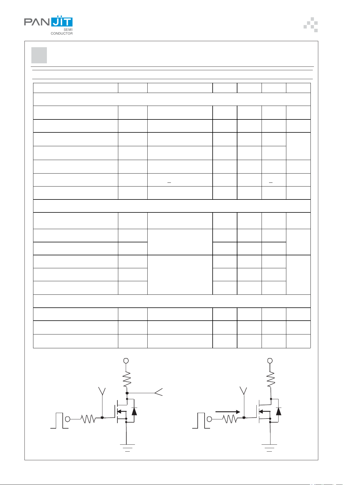
Test Circuit
V
IN
R
G
SD
I
s
I
sM
V
DD
IS=200mA , VGS=0V - 0.82 1.3 V
---115mA
---800mA
V
Gate Charge
DD
Test Circuit
R
L
V
OUT
1mA
V
GS
R
G
R
L
PAGE . 2May 21.2010-REV.01
Page 3
2N7002KDW
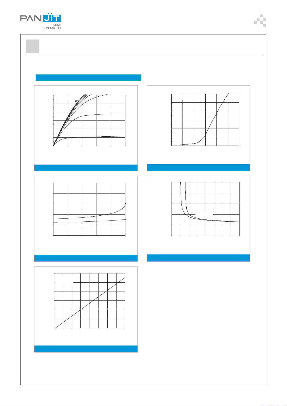
Typical Characteristics Curves (T =25 C,unless otherwise noted)
A
O
0
0.2
0.4
0.6
0.8
1
1.2
012345
VDS- Drain-to-Source Voltage (V)
I
D
- Drain-to-Source Current (A)
VGS= 6.0~10V
5.0V
4.0V
3.0V
0
1
2
3
4
5
2345678910
V
GS
- Gate -to-Source Voltage (V)
ID=200mA
ID=500mA
0
1
2
3
4
5
0 0.2 0.4 0 .6 0.8 1
ID-DrainCurrent(A)
VGS=4.5V
VGS=10V
0.6
0.8
1
1.2
1.4
1.6
1.8
-50 -25 0 25 50 75 100 125 150
TJ- Junction Temperature (oC)
R
DS(ON)
- On- Resistance( Normalized)
VGS=10V
I
D
=500mA
Typical Characteristics Curves (T =25 C,unless otherwise noted)
V = 10V~ 6.0V
GS
O
A
5.0V
4.0V
3.0V
Fig. 1-TYPICAL FORWARD CHARACTERISTIC
FIG.1- Output Characteristic
W
1.2
V =10V
DS
V =10V
DS
V =10V
DS
1
0.8
0.6
0.4
T =25
J ℃
T =25
J ℃
T =25
0.2
- Drain Source Current (A)
D
I
0
0123456
J ℃
VGS- Gate-to-Source Voltage (V)
FIG.2- Transfer Characteristic
W
V =10V
DS(ON)
R - On-Resistance ( )
FIG.3- On Resistance vs Drain Current
GS
FIG.5- On Resistance vs Junction Temperature
I =200mA
D
DS(ON)
R - On-Resistance ( )
FIG.4- On Resistance vs Gate to Source Voltage
PAGE . 3May 21.2010-REV.01
Page 4

2N7002KDW
72
74
76
78
80
82
84
86
88
-50 -25 0 25 50 75 100 125 150
TJ- Junction Temperature (oC)
BV
DSS
- Breakdown Voltage (V)
ID = 250uA
0.7
0.8
0.9
1
1.1
1.2
-50 -25 0 25 50 75 100 125 150
TJ- Junction Temperature (oC)
V
th
- G-S Threshold Voltage (NORMALIZED)
ID=250mA
Vgs
Vgs(th)
Qg(th)
Qsw
Qg
10
V =10V
DS
I =250mA
D
8
6
4
2
- Gate-to-Source Voltage (V)
GS
V
0
0 0.2 0.4 0.6 0.8 1
QgdQgs
Qg
Qg-GateCharge(nC)
Fig.6 - Gate Charge Waveform
Fig.8 - Threshold Voltage vs Temperature
10
V =0V
GS
1
25
-55
℃
℃
0.1
T =125
J
- Source Current (A)
S
I
0.01
0.2 0.4 0.6 0.8 1 1.2 1.4 1.6
℃
VSD- Source-to-Drain Voltage (V)
Fig.7 - Gate Charge
Fig.9 - Breakdown Voltage vs Junction Temperature
Fig.10 - Source-Drain Diode Forward Voltage
PAGE . 4May 21.2010-REV.01
Page 5

2N7002KDW
MOUNTING PAD LAYOUT
SOT-363
0.020
(0.50)
0.018
(0.45)
0.026
(0.65)
0.026
(0.65)
Unit inch(mm):
0.075
(1.90)
ORDER INFORMATION
• Packing information
T/R - 10K per 13" plastic Reel
T/R - 3K per 7” plastic Reel
LEGAL STATEMENT
Copyright PanJit International, Inc 2012
The information presented in this document is believed to be accurate and reliable. The specifications and information herein are
subject to change without notice. Pan Jit makes no warranty, representation or guarantee regarding the suitability of its produ cts for
any particular purpose. Pan Jit products are not authorized for use in life support devices or systems. Pan Jit does not convey any
license under its patent rights or rights of others.
May 21.2010-REV.01
PAGE . 5
Page 6

2N7002KDW
For example :
RB500V-40_R2_00001
Part No.
Packing Code XX Version Co de XXXXX
Serial number
Version code means HF
Packing size code means 13"
Packing type means T/R
Packing
type
st
1
Code
Packing
size code
nd
2
Code HF or RoHS 1st Code 2nd~5
T/B A N/A 0 HF 0 se rial n umbe r
T/R R 7" 1 RoHS 1 seria l numb er
B/P B 13" 2
T/P T 26mm X
TRR S 52mm Y
TRL L PBCU U
FORMING F PBCD D
Part No_packing code_Version
2N7002KDW_R1_00001
2N7002KDW_R2_00001
th
Code
May 21.2010-REV.01
PAGE . 6
Page 7

 Loading...