

2N7002K
60V N-Channel Enhancement Mode MOSFET - ESD Protected
FEATURES
• R
, VGS@10V,IDS@500mA=3Ω
DS(ON)
• R
, VGS@4.5V,IDS@200mA=4Ω
DS(ON)
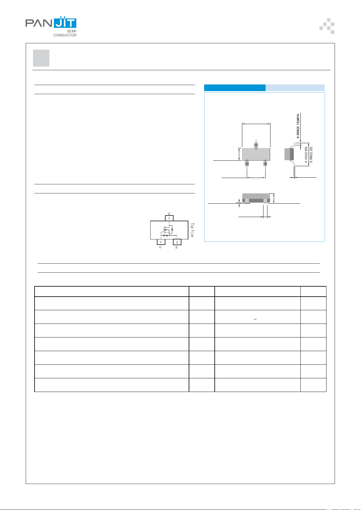
SOT-23
Unit inch(mm):
• Advanced Trench Process Technology
• High Density Cell Design For Ultra Low On-Resistance
0. 120 (3 .0 4)
0. 110( 2. 80)
• Very Low Leakage Current In Off Condition
• Specially Designed for Battery Operated Systems, Solid-State Relays
Drivers : Relays, Displays, Lamps, Solenoids, Memories, etc.
• ESD Protected 2KV HBM
0. 056 (1 .4 0)
0. 047 (1 .2 0)
• Lead free in comply with EU RoHS 2002/95/EC directives.
• Green molding compound as per IEC61249 Std. . (Halogen Free)
MECHANICAL
DATA
• Case: SOT-23 Package
• Terminals : Solderable per MIL-STD-750,Method 2026
• Apporx. Weight: 0.0003 ounces, 0.0084 grams
• Marking : K72
0. 079 (2 .0 0)
0. 070 (1 .8 0)
0. 004 (0 .1 0)
0. 000 (0 .0 0)
0. 020 (0 .5 0)
0. 013 (0 .3 5)
Maximum RATINGS and Thermal Characteristics (TA=25OC unless otherwise noted )
PARAMETER Symbol Limit Units
0. 008 (0 .2 0)
0. 003 (0 .0 8)
0. 044 (1 .1 0)
0. 035 (0 .9 0)
Drain-Source Voltage V
Gate-Source Voltage V
Co ntinuous D ra i n Curre nt I
Pulsed Drain Current
Maximum Po wer Dissipatio n
1)
T
=25OC
A
T
=75OC
A
Operating Junction and Storage Temperature Range T
Junction-to Ambient Thermal Resistance(PCB mounted)
2
DS
GS
D
I
DM
P
D
J,TSTG
R
θJA
60 V
+20 V
300 mA
2000 mA
350
210
-55 to + 150
357
Note: 1. Maximum DC current limited by the package
2. Surface mounted on FR4 board, t < 5 sec
PAN JIT RESERVES THE RIGHT TO IMPROVE PRODUCT DESIGN,FUNCTIONS AND RELIABILITY WITHOUT NOTICE
mW
O
O
C/W
C
PAGE . 1October 29,2010-REV.02
2N7002K
ELECTRICAL CHARACTERISTICS
Parameter Symbol Test Condition Min. Typ. Max. Units
Static
Drain-Source Breakdown Voltage BV
Gate Threshold Voltage V
Drain-Source On-State Resistance R
Drain-Source On-State Resistance R
Zero Gate Voltage Drain Current I
Gate Body Leakage I
Forward Transconductance g
Dynamic
Total Gate Charge Q
Tur n -On Ti me t
Tur n -Off Ti me t
Input Capacitance C
Reverse Transfer Capacitance C
DSS
GS(th)
DS(on)
DS(on)
DSS
GSS
fS
g
on
off
iss
oss
rss
VGS=0V , ID=10μ A60--V
VDS=V
, ID=250μ A1-2.5V
GS
VGS=4.5V , I D=200mA - - 4 .0
Ω
VGS=10V , I D=500mA - - 3.0
VDS=60V , VGS=0V --1μA
VGS=+20V , VDS=0V - - +10 μA
VDS=15V , ID=250mA 100 - - mS
VDS=15V, ID=200mA
V
=5V
GS
VDD=30V , RL=150Ω
I
=200mA , V
D
R
=10Ω
G
GEN
=10V
--0.8nC
--20
ns
--40
--35
VDS=25V , VGS=0V
f=1.0MH
Z
--10
pFOutput Capacitance C
--5
Source-Drain Di ode
Diode Forward Voltage V
Continuous Diode Forward Current I
Pulse Diode Forward Current I
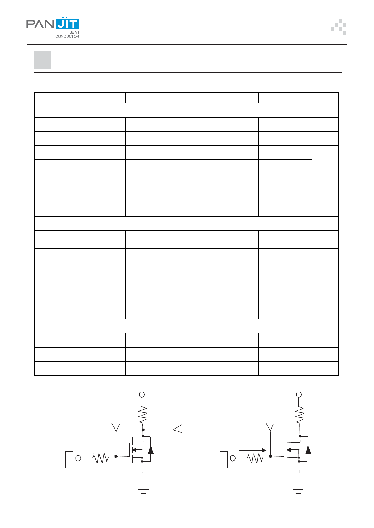
Switching
Test Circuit
V
IN
R
G
SD
S
SM
V
DD
IS=200mA , VGS=0V - 0.82 1.3 V
- - - 300 mA
- - - 2000 mA
V
Gate Charge
DD
Test Circuit
R
L
V
OUT
V
GS
1mA
R
G
R
L
PAGE . 2October 29,2010-REV.02
Fig. 1-TYPICAL FORWARD CHARACTERISTIC
FIG.1- Output Characteristic
Typical Characteristics Curves (T =25 C,unless otherwise noted)
A
O
FIG.2- Transfer Characteristic
FIG.3- On Resistance vs Drain Current
FIG.4- On Resistance vs Gate to Source Voltage
FIG.5- On Resistance vs Junction Temperature
VDS- Drain-to-Source Voltage (V)
I
D
- Drain-to-SourceCurrent (A)
VGS- Gate-to-Source Voltage (V)
I
D
- Drain Source Current (A)
ID- Drain Current (A)
R
DS(ON)
- On-Resistance
()W
VGS- Gate-to-Source Voltage (V)
R
DS(ON)
- On-Resistance
()W
TJ- Junction Temperature (oC)
R
DS(ON)
- On-Res istanc e(Nor malized)
0
0.2
0.4
0.6
0.8
1
1.2
012345
VGS= 6.0~10V
5.0V
4.0V
3.0V
0
0.2
0.4
0.6
0.8
1
1.2
0123456
VDS=10V
25oC
0
1
2
3
4
5
0 0.2 0.4 0.6 0.8 1
VGS=4.5V
VGS=10V
0
1
2
3
4
5
2345678910
ID=200mA
ID=500mA
0.6
0.8
1
1.2
1.4
1.6
1.8
-50 -25 0 25 50 75 100 125 150
VGS=10V
I
D
=500mA
2N7002K
PAGE . 3October 29,2010-REV.02

2N7002K
Vgs
Qg
Vgs(th)
Qg(th)
Qsw
QgdQgs
Fig.6 - Gate Charge Waveform
1.2
1.1
1
0.9
0.8
- G-S Threshold Voltage (NORMALIZED)
th
0.7
V
-50 -25 0 25 50 75 100 125 150
TJ- Junction Temperature ( C)
ID=250 Am
Qg
10
V
10V
DS=
8
=250mA
I
D
6
4
2
- Gate-t o -So u rce Vo ltage (V)
GS
V
0
0 0.2 0.4 0.6 0.8 1
Qg- Gate Charge (nC)
Fig.7 - Gate Charge
88
ID = 250 Am
86
84
82
80
78
76
- Breakdown Voltage (V)
74
DSS
BV
72
-50 -25 0 25 50 75 100 125 150
TJ- Junction Temperature (oC)
Fig.8 - Threshold Voltage vs Temperature
10
VGS=0V
1
TJ=125oC
0.1
- Source Current (A)
S
I
0.01
0.2 0.4 0.6 0.8 1 1.2 1.4 1.6
VSD- Source-to-Drain Voltage (V)
-55oC
25oC
Fig.10 - Source-Drain Diode Forward Voltage
Fig.9 - Breakdown Voltage vs Junction Temperature
70
60
50
40
30
20
C - Capacitance (pF)
10
Crss
0
0 5 10 15 20 25
Ciss
Coss
VDS- Drain-to-Source Voltage (V)
f=1MHz
=0V
V
GS
Fig.11 - Capacitance vs Drain to Source Voltage
PAGE . 4October 29,2010-REV.02

2N7002K
MOUNTING PAD LAYOUT
SOT-23
0.035 MIN.
(0.90) MIN.
0.043
(1.10)
0.106
(2.70)
0.031 MIN.
(0.80) MIN.
0.037
(0.95)
Unit inch(mm):
0.043
(1.10)
0.078
(2.00)
ORDER INFORMATION
• Packing information
T/R - 12K per 13" plastic Ree
T/R - 3K per 7” plastic Reel
l
October 29,2010-REV.02
PAGE . 5

2N7002K
Part No_packing code_Version
2N7002K_R1_00001
2N7002K_R2_00001
For example :
RB500V-40_R2_00001
Serial number
Part No.
Version code means HF
Packing size code means 13"
Packing type means T/R
Packing type 1st Code Packing size code 2nd Code HF or RoHS 1st Code 2nd~5
Tape and Ammunition Box
(T/B)
Tape and Reel
(T/R)
Bulk Packing
(B/P)
Tube Packing
(T/P)
Tape and Reel (Right Oriented)
(TRR)
Tape and Reel (Left Oriented)
(TRL)
FORMING F
Packing Code XX Version Code XXXXX
th
Code
A N/A 0 HF 0 serial number
R 7" 1 RoHS 1 serial number
B 13" 2
T 26mm X
S 52mm Y
PANASERT T/B CATHODE UP
L
PANASERT T/B CATHODE DOWN
(PBCU)
(PBCD)
U
D
October 29,2010-REV.02
PAGE . 6

2N7002K
Disclaimer
z Reproducing and modifying information of the document is prohibited without
permission from Panjit International Inc..
z Panjit International Inc. reserves the rights to make changes of the content herein the
document anytime without notification. Please refer to our website for the latest
document.
z Panjit International Inc. disclaims any and all liability arising out of the application or
use of any product including damages incidentally and consequentially occurred.
z Panjit International Inc. does not assume any and all implied warranties, including
warranties of fitness for particular purpose, non-infringement and merchantability.
z Applications shown on the herein document are examples of standard use and
operation. Customers are responsible in comprehending the suitable use in particular
applications. Panjit International Inc. makes no representation or warranty that such
applications will be suitable for the specified use without further testing or modification.
z The products shown herein are not designed and authorized for equipments requiring
high level of reliability or relating to human life and for any applications concerning
life-saving or life-sustaining, such as medical instruments, transportation equipment,
aerospace machinery et cetera. Customers using or selling these products for use in
such applications do so at their own risk and agree to fully indemnify Panjit
International Inc. for any damages resulting from such improper use or sale.
October 29,2010-REV.02
PAGE . 7

 Loading...